KSZ8873MLL-EVAL
Microchip Technology Inc.Ethernet Development Tools 3-Port Fast Ethernet Switch with 1x MII Interface - Evaluation Board

KSZ9031MNX-EVAL
Microchip Technology Inc.Ethernet Development Tools 1-Port Gigabit Ethernet PHY - Evaluation Board
KSZ9031MNX-EVAL
Microchip Technology Inc.Ethernet Development Tools 1-Port Gigabit Ethernet PHY - Evaluation Board


KSZ8795CLXD-EVAL
Microchip Technology Inc.Ethernet Development Tools 5-Port 10/100 with RGMII/GMII - Evaluation Board
KSZ8863FLL-EVAL
Microchip Technology Inc.Ethernet Development Tools 3-Port 10/100 Ethernet Switch with 1x FX Port and 1x TX Port - Evaluation Board
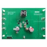
EVQ4210-U-00B
Monolithic Power Systems (MPS)40V, USB Type-C PD, Synchronous, Buck-Boost Controller with I2C Evaluation Board

EVM3YSX50B14
Panasonic10 kOhms 0.15W J Lead Surface Mount Trimmer Potentiometer Cermet 1.0 Turn Top Adjustment

EVAL-AD7794EBZ
Analog Devices Inc.The AD7794/AD7795 are low power, low noise, complete analog front ends for high precision measurement applications. They contain a low noise, 24-/16-bit ?-? ADC with six differential inputs. The on-chip low noise instrumentation amplifier means that signals of small amplitude can be interfaced directly to the ADC.Each device contains a precision, low noise, low drift internal band gap reference, and can also accept up to two external differential references. Other on-chip features include programmable excitation current sources, burnout currents, and a bias voltage generator that is used to set the common-mode voltage of a channel to AVDD/2. The low-side power switch can be used to power down bridge sensors between conversions, minimizing the system?s power consumption. The AD7794/AD7795 can operate with either an internal clock or an external clock. The output data rate from each part can vary from 4.17 Hz to 470 Hz.Both parts operate with a power supply from 2.7 V to 5.25 V. The B-grade parts (AD7794 and AD7795) are specified for a temperature range of ?40?C to +105?C while the C-grade part (AD7794) is specified for a temperature range of ?40?C to +125?C. They consume a current of 400 ?A typical and are housed in a 24-lead TSSOP.Applications Temperature measurement Pressure measurement Weigh scales Strain gage transducers Gas analysis
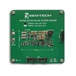
TSDMRX-19V-20W-EVM
Semtech CorporationPower Management IC Development Tools WP DUAL MODE RX UP TO 20W, 19V

KSZ9031MNX-EVAL
Microchip Technology Inc.Ethernet Development Tools 1-Port Gigabit Ethernet PHY - Evaluation Board

STEVAL-ISA206V1
STMicroelectronicsPower Management IC Development Tools 38 V, 2 A synchronous step-down switching regulator evaluation board based on L6986H STEVAL-ISA206V1

KSZ8851-16MLL-EVAL
Microchip Technology Inc.Ethernet Development Tools Single Ethernet Port + Generic (16-bit) Bus Interface Eval Board


