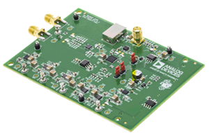
ADS54RF63_ADX4
Texas InstrumentsData Conversion IC Development Tools 2.2GSPS Interleaved ADC Eval Mod
LM2852Y-2.5EVAL
Texas InstrumentsPower Management IC Development Tools 2A 500/1500kHz Synchronous SIMPLE SWITCH
STEVAL-SMARTAG1
STMicroelectronicsRF Development Tools NFC Dynamic Tag sensor node evaluation board
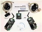
EVAL-PAN1740
Panasonic Industrial DevicesBluetooth Development Tools (802.15.1) PAN1740 EVALUATION KIT
AD9572-EVALZ-PEC
Analog Devices Inc.The AD9572 provides a multioutput clock generator function along with two on-chip PLL cores, optimized for fiber channel line card applications that include an Ethernet interface. The integer-N PLL design is based on the Analog Devices, Inc., proven portfolio of high performance, low jitter frequencysynthesizers to maximize network performance. Other applications with demanding phase noise and jitter requirements also benefit from this part. The PLL section consists of a low noise phase frequency detector (PFD), a precision charge pump (CP), a low phase noise voltage controlled oscillator (VCO), and a preprogrammed feedback divider and output divider. By connecting an external crystal or reference clock to the REFCLK pin, frequencies up to 156.25 MHz can be locked to the input reference. Each output divider and feedback divider ratio is preprogrammed for therequired output rates. A second PLL also operates as an integer-N synthesizer anddrives two LVPECL or LVDS output buffers for 106.25 MHzoperation. No external loop filter components are required, thusconserving valuable design time and board space. The AD9572 is available in a 40-lead, 6 mm ? 6 mm lead framechip scale package (LFCSP) and can be operated from a single3.3 V supply. The temperature range is ?40?C to +85?C.APPLICATIONSFiber channel line cards, switches, and routersGigabit Ethernet/PCIe support included Low jitter, low phase noise clock generation
AD9609-20EBZ
Analog Devices Inc.The AD9609 is a monolithic, single channel 1.8 V supply, 10-bit,20/40/65/80 MSPS analog-to-digital converter (ADC). It featuresa high performance sample-and-hold circuit and on-chip voltagereference.The product uses multistage differential pipeline architecturewith output error correction logic to provide 10-bit accuracy at80 MSPS data rates and to guarantee no missing codes over thefull operating temperature range.The ADC contains several features designed to maximize flexibilityand minimize system cost, such as programmable clock and dataalignment and programmable digital test pattern generation. Theavailable digital test patterns include built-in deterministic andpseudorandom patterns, along with custom user-defined testpatterns entered via the serial port interface (SPI).A differential clock input with selectable internal 1 to 8 divide ratiocontrols all internal conversion cycles. An optional duty cyclestabilizer (DCS) compensates for wide variations in the clock dutycycle while maintaining excellent overall ADC performance.The digital output data is presented in offset binary, gray code, ortwos complement format. A data output clock (DCO) is providedto ensure proper latch timing with receiving logic. Both 1.8 V and3.3 V CMOS levels are supported.The AD9609 is available in a 32-lead RoHS-compliant LFCSPand is specified over the industrial temperature range (?40?Cto +85?C).APPLICATIONS Communications Diversity radio systems Multimode digital receivers GSM, EDGE, W-CDMA, LTE, CDMA2000, WiMAX, TD-SCDMA Smart antenna systems Battery-powered instruments Handheld scope meters Portable medical imaging Ultrasound Radar/LIDAR PET/SPECT imagingPRODUCT HIGHLIGHTS1. The AD9609 operates from a single 1.8 V analog powersupply and features a separate digital output driver supplyto accommodate 1.8 V to 3.3 V logic families.2. The sample-and-hold circuit maintains excellent performancefor input frequencies up to 200 MHz and is designed for lowcost, low power, and ease of use.3. A standard serial port interface supports various productfeatures and functions, such as data output formatting,internal clock divider, power-down, DCO and data output(D9 to D0) timing and offset adjustments, and voltagereference modes.4. The AD9609 is packaged in a 32-lead RoHS compliantLFCSP that is pin compatible with the AD9629 12-bit ADCand the AD9649 14-bit ADC, enabling a simple migrationpath between 10-bit and 14-bit converters sampling from20 MSPS to 80 MSPS.
AD9625-2.0EBZ
Analog Devices Inc.The AD9625 is a 12-bit monolithic sampling analog-to-digital converter (ADC) that operates at conversion rates of up to 2.6 giga samples per second (GSPS). This product is designed for sampling wide bandwidth analog signals up to the second Nyquist zone. The combination of wide input bandwidth, high sampling rate, and excellent linearity of the AD9625 is ideally suited for spectrum analyzers, data acquisition systems, and a wide assortment of military electronics applications, such as radar and jamming/antijamming measures.The analog input, clock, and SYSREF? signals are differential inputs. The JESD204B-based high speed serialized output is configurable in a variety of one-, two-, four-, six-, or eight-lane configurations. The product is specified over the industrial temperature range of ?40?C to +85?C.PRODUCT HIGHLIGHTS High performance: exceptional SFDR in high sample rate applications, direct RF sampling, and on-chip reference. Flexible digital data output formats based on the JESD204B specification. Control path SPI interface port that supports various product features and functions, such as data formatting, gain, and offset calibration values.APPLICATIONS Spectrum analyzers Military communications Radar High performance digital storage oscilloscopes Active jamming/antijamming Electronic surveillance and countermeasures
AD9635-125EBZ
Analog Devices Inc.The AD9635 is a dual, 12-bit, 80 MSPS/125 MSPS analog-to-digital converter (ADC) with an on-chip sample-and-hold circuit designed for low cost, low power, small size, and ease of use. The product operates at a conversion rate of up to 125 MSPS and is optimized for outstanding dynamic performance and low power in applications where a small package size is critical.The ADC requires a single 1.8 V power supply and LVPECL-/ CMOS-/LVDS-compatible sample rate clock for full performanceoperation. No external reference or driver components arerequired for many applications.The ADC automatically multiplies the sample rate clock for theappropriate LVDS serial data rate. A data clock output (DCO) for capturing data on the output and a frame clock output (FCO) forsignaling a new output byte are provided. Individual channelpower-down is supported; the AD9635 typically consumes lessthan 2 mW in the full power-down state. The ADC providesseveral features designed to maximize flexibility and minimize system cost, such as programmable output clock and data alignment and digital test pattern generation. The available digital test patterns include built-in deterministic and pseudorandom patterns, along with custom user-defined test patterns entered via the serial port interface (SPI).The AD9635 is available in a RoHS-compliant, 32-lead LFCSP. It is specified over the industrial temperature range of ?40?Cto +85?C. PRODUCT HIGHLIGHTS Small Footprint. Two ADCs are contained in a small, spacesaving package. Low Power. The AD9635 uses 115 mW/channel at 125 MSPS with scalable power options. Pin Compatibility with the AD9645, a 14-Bit Dual ADC. Ease of Use. A data clock output (DCO) operates at frequencies of up to 500 MHz and supports double data rate (DDR) operation. User Flexibility. The SPI control offers a wide range of flexible features to meet specific system requirements. APPLICATIONS Communications Diversity radio systems Multimode digital receivers GSM, EDGE, W-CDMA, LTE, CDMA2000, WiMAX, TD-SCDMA I/Q demodulation systems Smart antenna systems Broadband data applications Battery-powered instruments Hand held scope meters Portable medical imaging and ultrasound Radar/LIDAR
AD9649-80EBZ
Analog Devices Inc.The AD9649 is a monolithic, single channel 1.8 V supply, 14-bit, 20/40/65/80 MSPS analog-to-digital converter (ADC). It features a high performance sample-and-hold circuit and an on-chip volt-age reference.The product uses multistage differential pipeline architecture with output error correction logic to provide 14-bit accuracy at 80 MSPS data rates and to guarantee no missing codes over the full operating temperature range.The ADC contains several features designed to maximize flexibility and minimize system cost, such as programmable clock and data alignment and programmable digital test pattern generation. The available digital test patterns include built-in deterministic and pseudorandom patterns, along with custom user-defined test patterns entered via the serial port interface (SPI).A differential clock input with optional 1, 2, or 4 divide ratios controls all internal conversion cycles.The digital output data is presented in offset binary, gray code, or twos complement format. A data output clock (DCO) is provided to ensure proper latch timing with receiving logic. Both 1.8 V and 3.3 V CMOS levels are supported.The AD9649 is available in a 32-lead RoHS-compliant LFCSP and is specified over the industrial temperature range (?40?C to +85?C).PRODUCT HIGHLIGHTS The AD9649 operates from a single 1.8 V analog power supply and features a separate digital output driver supply to accommodate 1.8 V to 3.3 V logic families. The sample-and-hold circuit maintains excellent performance for input frequencies up to 200 MHz and is designed for low cost, low power, and ease of use. A standard serial port interface (SPI) supports various product features and functions, such as data output formatting, internal clock divider, power-down, DCO, data output (D13 to D0) timing and offset adjustments, and voltage reference modes. The AD9649 is packaged in a 32-lead RoHS-compliant LFCSP that is pin compatible with the AD9629 12-bit ADC and the AD9609 10-bit ADC, enabling a simple migration path between 10-bit and 14-bit converters sampling from 20 MSPS to 80 MSPS.?APPLICATIONS Communications Diversity radio systems Multimode digital receivers GSM, EDGE, W-CDMA, LTE, CDMA2000, WiMAX, TD-SCDMA Smart antenna systems Battery-powered instruments Handheld scope meters Portable medical imaging Ultrasound Radar/LIDAR
AD9680-1000EBZ
Analog Devices Inc.The AD9680 is a dual, 14-bit, 1.25 GSPS/1 GSPS/820 MSPS/500 MSPS analog-to-digital converter (ADC). The device has an on-chip buffer and sample-and-hold circuit designed for low power, small size, and ease of use. This device is designed for sampling wide bandwidth analog signals of up to 2 GHz. The AD9680 is optimized for wide input bandwidth, high sampling rate, excellent linearity, and low power in a small package.The dual ADC cores feature a multistage, differential pipelined architecture with integrated output error correction logic. Each ADC features wide bandwidth inputs supporting a variety of user-selectable input ranges. An integrated voltage reference eases design considerations.The analog input and clock signals are differential inputs. Each ADC data output is internally connected to two digital down-converters (DDCs). Each DDC consists of up to five cascaded signal processing stages: a 12-bit frequency translator (NCO), and four half-band decimation filters. The DDCs are bypassed by default.In addition to the DDC blocks, the AD9680 has several functions that simplify the automatic gain control (AGC) function in the communications receiver. The programmable threshold detector allows monitoring of the incoming signal power using the fast detect output bits of the ADC. If the input signal level exceeds the programmable threshold, the fast detect indicator goes high. Because this threshold indicator has low latency, the user can quickly turn down the system gain to avoid an overrange condition at the ADC input.Users can configure the Subclass 1 JESD204B-based high speed serialized output in a variety of one-, two-, or four-lane configurations, depending on the DDC configuration and the acceptable lane rate of the receiving logic device. Multiple device synchronization is supported through the SYSREF? and SYNCINB? input pins.The AD9680 has flexible power-down options that allow significant power savings when desired. All of these features can be programmed using a 1.8 V to 3.3 V capable, 3-wire SPI.The AD9680 is available in a Pb-free, 64-lead LFCSP and is specified over the ?40?C to +85?C industrial temperature range. This product is protected by a U.S. patent.PRODUCT HIGHLIGHTS Wide full power bandwidth supports IF sampling of signals up to 2 GHz. Buffered inputs with programmable input termination eases filter design and implementation. Four integrated wideband decimation filters and numerically controlled oscillator (NCO) blocks supporting multiband receivers. Flexible serial port interface (SPI) controls various product features and functions to meet specific system requirements. Programmable fast overrange detection. 9 mm ? 9 mm, 64-lead LFCSP.APPLICATIONS Communications Diversity multiband, multimode digital receivers 3G/4G, TD-SCDMA, W-CDMA, GSM, LTE General-purpose software radios Ultrawideband satellite receivers Instrumentation Radars Signals intelligence (SIGINT) DOCSIS 3.0 CMTS upstream receive paths HFC digital reverse path receivers
AD9680-1250EBZ
Analog Devices Inc.The AD9680 is a dual, 14-bit, 1.25 GSPS/1 GSPS/820 MSPS/500 MSPS analog-to-digital converter (ADC). The device has an on-chip buffer and sample-and-hold circuit designed for low power, small size, and ease of use. This device is designed for sampling wide bandwidth analog signals of up to 2 GHz. The AD9680 is optimized for wide input bandwidth, high sampling rate, excellent linearity, and low power in a small package.The dual ADC cores feature a multistage, differential pipelined architecture with integrated output error correction logic. Each ADC features wide bandwidth inputs supporting a variety of user-selectable input ranges. An integrated voltage reference eases design considerations.The analog input and clock signals are differential inputs. Each ADC data output is internally connected to two digital down-converters (DDCs). Each DDC consists of up to five cascaded signal processing stages: a 12-bit frequency translator (NCO), and four half-band decimation filters. The DDCs are bypassed by default.In addition to the DDC blocks, the AD9680 has several functions that simplify the automatic gain control (AGC) function in the communications receiver. The programmable threshold detector allows monitoring of the incoming signal power using the fast detect output bits of the ADC. If the input signal level exceeds the programmable threshold, the fast detect indicator goes high. Because this threshold indicator has low latency, the user can quickly turn down the system gain to avoid an overrange condition at the ADC input.Users can configure the Subclass 1 JESD204B-based high speed serialized output in a variety of one-, two-, or four-lane configurations, depending on the DDC configuration and the acceptable lane rate of the receiving logic device. Multiple device synchronization is supported through the SYSREF? and SYNCINB? input pins.The AD9680 has flexible power-down options that allow significant power savings when desired. All of these features can be programmed using a 1.8 V to 3.3 V capable, 3-wire SPI.The AD9680 is available in a Pb-free, 64-lead LFCSP and is specified over the ?40?C to +85?C industrial temperature range. This product is protected by a U.S. patent.PRODUCT HIGHLIGHTS Wide full power bandwidth supports IF sampling of signals up to 2 GHz. Buffered inputs with programmable input termination eases filter design and implementation. Four integrated wideband decimation filters and numerically controlled oscillator (NCO) blocks supporting multiband receivers. Flexible serial port interface (SPI) controls various product features and functions to meet specific system requirements. Programmable fast overrange detection. 9 mm ? 9 mm, 64-lead LFCSP.APPLICATIONS Communications Diversity multiband, multimode digital receivers 3G/4G, TD-SCDMA, W-CDMA, GSM, LTE General-purpose software radios Ultrawideband satellite receivers Instrumentation Radars Signals intelligence (SIGINT) DOCSIS 3.0 CMTS upstream receive paths HFC digital reverse path receivers
AD9684-500EBZ
Analog Devices Inc.The AD9684 is a dual, 14-bit, 500 MSPS ADC. The device has an on-chip buffer and a sample-and-hold circuit designed for low power, small size, and ease of use. This product is designed for sampling wide bandwidth analog signals. The AD9684 is optimized for wide input bandwidth, a high sampling rate, excellent linearity, and low power in a small package.The dual ADC cores feature a multistage, differential pipelined architecture with integrated output error correction logic. Each ADC features wide bandwidth buffered inputs, supporting a variety of user selectable input ranges. An integrated voltage reference eases design considerations. Each ADC data output is internally connected to an optional decimate by 2 block.The analog input and clock signals are differential inputs. Each ADC data output is internally connected to two digital downconverters (DDCs). Each DDC consists of four cascaded signal processing stages: a 12-bit frequency translator (NCO), and three half-band decimation filters supporting a divide by factor of two, four, and eight.Applications Communications Diversity multi-band, multi-mode digital receivers 3G/4G, TD-SCDMA, WCDMA, MC-GSM, LTE General-purpose software radios Ultrawideband satellite receiver Instrumentation (spectrum analyzers, network analyzers, integrated RF test solutions) Radar Digital oscilloscopes High speed data acquisition systems DOCSIS CMTS upstream receive paths HFC digital reverse path receivers
AD9689-2600EBZ
Analog Devices Inc.The AD9689 is a dual, 14-bit, 2.0 GSPS/2.6 GSPS analog-to-digital converter (ADC). The device has an on-chip buffer and a sample-and-hold circuit designed for low power, small size, and ease of use. This product is designed to support communications applications capable of direct sampling wide bandwidth analog signals of up to 5 GHz. The ?3 dB bandwidth of the ADC input is 9 GHz. The AD9689 is optimized for wide input bandwidth, high sampling rate, excellent linearity, and low power in a small package.The dual ADC cores feature a multistage, differential pipelined architecture with integrated output error correction logic. Each ADC features wide bandwidth inputs supporting a variety of user-selectable input ranges. An integrated voltage reference eases design considerations. The analog input and clock signals are differential inputs. The ADC data outputs are internally connected to four digital downconverters (DDCs) through a crossbar mux. Each DDC consists of multiple cascaded signal processing stages: a 48-bit frequency translator (numerically controlled oscillator (NCO)), and decimation rates. The NCO has the option to select preset bands over the general-purpose input/output (GPIO) pins, which enables the selection of up to three bands. Operation of the AD9689 between the DDC modes is selectable via SPI-programmable profiles.In addition to the DDC blocks, the AD9689 has several functions that simplify the automatic gain control (AGC) function in a communications receiver. The programmable threshold detector allows monitoring of the incoming signal power using the fast detect control bits in Register 0x0245 of the ADC. If the input signal level exceeds the programmable threshold, the fast detect indicator goes high. Because this threshold indicator has low latency, the user can quickly turn down the system gain to avoid an overrange condition at the ADC input. In addition to the fast detect outputs, the AD9689 also offers signal monitoring capability. The signal monitoring block provides additional information about the signal being digitized by the ADC.The user can configure the Subclasss 1 JESD204B-based high speed serialized output in a variety of one-lane, two-lane, four-lane, and eight-lane configurations, depending on the DDC configuration and the acceptable lane rate of the receiving logic device. Multidevice synchronization is supported through the SYSREF? and SYNCINB? input pins.The AD9689 has flexible power-down options that allow significant power savings when desired. All of these features can be programmed using a 3-wire serial port interface (SPI).The AD9689 is available in a Pb-free, 196-ball BGA, specified over the ?40?C to +85?C ambient temperature range. This product is protected by a U.S. patent.Note that throughout this data sheet, multifunction pins, such as FD_A/GPIO_A0, are referred to either by the entire pin name or by a single function of the pin, for example, FD_A, when only that function is relevant.Product Highlights Wide, input ?3 dB bandwidth of 9 GHz supports direct radio frequency (RF) sampling of signals up to about 5 GHz. Four integrated, wideband decimation filters and NCO blocks supporting multiband receivers. Fast NCO switching enabled through the GPIO pins. SPI controls various product features and functions to meet specific system requirements. Programmable fast overrange detection and signal monitoring. On-chip temperature diode for system thermal management. 12 mm ? 12 mm, 196-ball BGA. Pin, package, feature, and memory map compatible with the AD9208 14-bit, 3.0 GSPS, JESD204B dual ADC.Applications Diversity multiband and multimode digital receivers 3G/4G, TD-SCDMA, W-CDMA, and GSM, LTE, LTE-A Electronic test and measurement systems Phased array radar and electronic warfare DOCSIS 3.0 CMTS upstream receive paths HFC digital reverse path receivers
AD9705-DPG2-EBZ
Analog Devices Inc.The AD9704/AD9705/AD9706/AD9707 are the fourth-generation family in the TxDAC series of high performance, CMOS digital-to-analog converters (DACs). This pin-compatible, 8-/10-/12-/14-bit resolution family is optimized for low power operation, while maintaining excellent dynamic performance. The AD9704/AD9705/AD9706/AD9707 family is pin-compatible with the AD9748/AD9740/AD9742/AD9744 family of TxDAC converters and is specifically optimized for the transmit signal path of communication systems. All of the devices share the same interface, LFCSP package, and pinout, providing an upward or downward component selection path based on performance, resolution, and cost. The AD9704/AD9705/AD9706/AD9707 offers exceptional ac and dc performance, while supporting update rates up to 175 MSPS.The flexible power supply operating range of 1.7 V to 3.6 V and low power dissipation of the AD9704/AD9705/AD9706/AD9707 parts make them well suited for portable and low power applications.Power dissipation of the AD9704/AD9705/AD9706/AD9707 can be reduced to 15 mW, with a small trade-off in performance, by lowering the full-scale current output. In addition, a power-down mode reduces the standby power dissipation to approximately 2.2 mW.The AD9704/AD9705/AD9706/AD9707 has an optional serial peripheral interface (SPI?) that provides a higher level of programmability to enhance performance of the DAC. An adjustable output, common-mode feature allows for easy interfacing to other components that require common modes from 0 V to 1.2 V.Edge-triggered input latches and a 1.0 V temperature-compensated band gap reference have been integrated to provide a complete, monolithic DAC solution. The digital inputs support 1.8 V and 3.3 V CMOS logic families.PRODUCT HIGHLIGHTS Pin Compatible. The AD9704/AD9705/AD9706/AD9707 line of TxDAC?converters is pin-compatible with theAD9748/AD9740/AD9742/AD9744 TxDAC line (LFCSP package). Low Power. Complete CMOS DAC operates on a single supply of 3.6 V down to 1.7 V, consuming 50 mW (3.3 V) and 12 mW (1.8 V). The DAC full-scale current can be reduced for lower power operation. Sleep and power-down modes are provided for low power idle periods. Self-Calibration. Self-calibration enables true 14-bit INL and DNL performance in the AD9707. Twos Complement/Binary Data Coding Support. Data input supports twos complement or straight binary data coding. Flexible Clock Input. A selectable high speed, single-ended,and differential CMOS clock input supports 175 MSPS conversion rate. Device Configuration. Device can be configured through pin strapping, and SPI control offers a higher level of programmability. Easy Interfacing to Other Components. Adjustable common-mode output allows for easy interfacing to other signal chain components that accept common-mode levels from 0 V to 1.2 V. On-Chip Voltage Reference. The AD9704/AD9705/AD9706/AD9707 include a 1.0 V temperature-compensated band gap voltage reference. Industry-Standard 32-Lead LFCSP Package.

