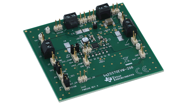
Ultra Low Power Management IC; Boost Charger Nanopowered Buck Converter Evaluation Module
Texas InstrumentsUltra Low Power Management IC; Boost Charger Nanopowered Buck Converter Evaluation Module


LMP92066EVM Evaluation Module for Dual; Temperature Controlled DAC with Integrated EEPROM
Texas InstrumentsLMP92066EVM Evaluation Module for Dual; Temperature Controlled DAC with Integrated EEPROM

3-pin adjustable regulator evaluation module
Texas Instruments3-pin adjustable regulator evaluation module

Arduino based Wireless Development Platform for Internet of Things applications based on an ultra-low power ARM Cortex-M3 processor
Analog Devices Inc.The EVAL-ADICUP3029 is an Arduino and PMOD compatible form factor development board that includes Bluetooth and WiFi connectivity. The board uses CrossCore Embedded Studio, an open source Eclipse based Interactive Development Environment (IDE), which can be downloaded free of charge. The platform contains many hardware and software example projects to make it easier for customers to prototype and create connected systems and solutions for Internet of Things (IoT) applications.
The EVAL-ADICUP3029 uses the ADuCM3029 ultra low power Arm Cortex-M3 processor as the main device on board. The ADuCM3029 is an integrated mixed-signal microcontroller system for processing, control and connectivity.


MSP-TS430PM64A - 64-pin Target Development Board for MSP430F4x MCUs
Texas InstrumentsMSP-TS430PM64A - 64-pin Target Development Board for MSP430F4x MCUs
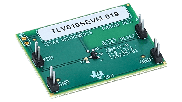
TLV810 3-pin voltage supervisor (reset IC) with active-high push-pull reset evaluation module
Texas InstrumentsTLV810 3-pin voltage supervisor (reset IC) with active-high push-pull reset evaluation module


MSP-TS430RHA40A- 40-pin Target Development Board for MSP430FRxx FRAM MCUs
Texas InstrumentsMSP-TS430RHA40A- 40-pin Target Development Board for MSP430FRxx FRAM MCUs

BQ24292IEVM-021 Single Cell Charger with Narrow VDC Power Path Management Evaluation Module
Texas InstrumentsBQ24292IEVM-021 Single Cell Charger with Narrow VDC Power Path Management Evaluation Module


UCD3138 Programmable Digital Power Controller Open Loop Evaluation Module (64-pin version)
Texas InstrumentsUCD3138 Programmable Digital Power Controller Open Loop Evaluation Module (64-pin version)


