
Evaluation Module for Dual; 200mA Output; Low Noise; High PSRR; Low-Dropout Regulator
Texas InstrumentsEvaluation Module for Dual; 200mA Output; Low Noise; High PSRR; Low-Dropout Regulator

I2C Controlled 3A Single Cell USB NVDC-1 Charger with Adjustable Voltage USB OTG Evaluation Module
Texas InstrumentsI2C Controlled 3A Single Cell USB NVDC-1 Charger with Adjustable Voltage USB OTG Evaluation Module


TI-PMLK Buck Experiment Board using TPS54160 & LM3475
Texas InstrumentsTI-PMLK Buck Experiment Board using TPS54160 & LM3475


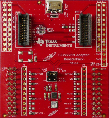
CC3220SF LaunchPad™ development kit for Wi-Fi® SimpleLink™ wireless MCU
Texas InstrumentsCC3220SF LaunchPad™ development kit for Wi-Fi® SimpleLink™ wireless MCU

OPT3001 digital ambient light sensor (ALS) with high-precision human-eye response evaluation module
Texas InstrumentsOPT3001 digital ambient light sensor (ALS) with high-precision human-eye response evaluation module
EVAL-PAN1740
Panasonic Industrial DevicesBluetooth/802.15.1 Development Tools PAN1740 EVALUATION KIT
ISL8088EVAL2Z
Renesas Electronics CorporationDC-DC Step Down 2 Non-Isolated Outputs ISL8088 Evaluation Board

ISL8225MEVAL4Z
Renesas Electronics CorporationEvaluation Board for ISL8225M Dual 15 A Single 30 A Step-Down Power Module


INA1620 Audio Operational Amplifier Evaluation Module
Texas InstrumentsINA1620 Audio Operational Amplifier Evaluation Module
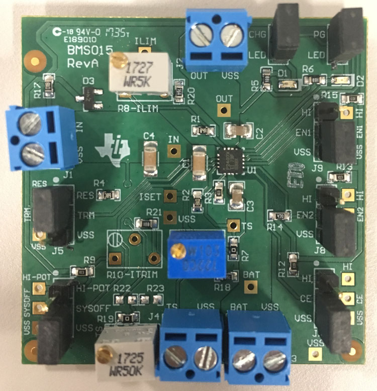
bq24078 1.5A Single-Chip Li-Ion and Li-Polymer Charger Management IC Evaluation Module
Texas Instrumentsbq24078 1.5A Single-Chip Li-Ion and Li-Polymer Charger Management IC Evaluation Module


