Manufacturer
MORE
Stock

Displaying 261 - 280 of 11821

Evaluation Kits

ADP2107-EVALZ

Analog Devices Inc.
The ADP2105 / ADP2106 / ADP2107 are low quiescent current,synchronous, step-down dc-to-dc converters in a compact 4 mm ?4 mm LFCSP package. At medium to high load currents, thesedevices use a current mode, constant frequency pulse-widthmodulation (PWM) control scheme for excellent stability andtransient response. To ensure the longest battery life in portableapplications, the ADP2105 / ADP2106 / ADP2107 use a pulsefrequency modulation (PFM) control scheme under light loadconditions that reduces switching frequency to save power.The ADP2105 / ADP2106 / ADP2107 run from input voltages of2.7 V to 5.5 V, allowing single Li+/Li? polymer cell, multiplealkaline/NiMH cells, PCMCIA, and other standard power sources.The output voltage of ADP2105 / ADP2106 / ADP2107 is adjustablefrom 0.8 V to the input voltage (indicated by ADJ), whereas theADP2105 / ADP2106 / ADP2107 are available in preset outputvoltage options of 3.3 V, 1.8 V, 1.5 V, and 1.2 V (indicated by x.x V).Each of these variations is available in three maximum currentlevels: 1 A (ADP2105), 1.5 A (ADP2106), and 2 A (ADP2107).The power switch and synchronous rectifier are integrated forminimal external part count and high efficiency. During logiccontrolled shutdown, the input is disconnected from the output,and it draws less than 0.1 ?A from the input source. Other keyfeatures include undervoltage lockout to prevent deep batterydischarge and programmable soft start to limit inrush current atstartup.Applications Mobile handsets PDAs and palmtop computers Telecommunication/networking equipment Set top boxes Audio/video consumer electronics

ADP2108-1.5-EVALZ

Analog Devices Inc.
The ADP2108 is a high efficiency, low quiescent current step-down dc-to-dc converter manufactured in two different packages. The total solution requires only three tiny external components. It uses a proprietary, high speed current mode, constant frequency PWM control scheme for excellent stability and transient response. To ensure the longest battery life in portable applications, the ADP2108 has a power save mode that reduces the switching frequency under light load conditions.The ADP2108 runs on input voltages of 2.3 V to 5.5 V, which allows for single lithium or lithium polymer cell, multiple alkaline or NiMH cell, PCMCIA, USB, and other standard power sources. The maximum load current of 600 mA is achievable across the input voltage range.The ADP2108 is available in fixed output voltages of 3.3 V, 3.0 V, 2.5 V, 2.3 V, 1.82 V, 1.8 V, 1.5 V, 1.3 V, 1.2 V, 1.1 V, and 1.0 V. All versions include an internal power switch and synchronous rectifier for minimal external part count and high efficiency. The ADP2108 has an internal soft start and is internally compensated. During logic controlled shutdown, the input is disconnected from the output and the ADP2108 draws less than 1 ?A from the input source.Other key features include undervoltage lockout to prevent deep battery discharge and soft start to prevent input current over-shoot at startup. The ADP2108 is available in 5-ball WLCSP and 5-lead TSOT packages. The ADP2109 provides the same features and operations as the ADP2108 and has the additional function of a discharge switch in the WLCSP package.APPLICATIONS PDAs and palmtop computers Wireless handsets Digital audio, portable media players Digital cameras, GPS navigation units

ADP2108-1.8-EVALZ

Analog Devices Inc.
The ADP2108 is a high efficiency, low quiescent current step-down dc-to-dc converter manufactured in two different packages. The total solution requires only three tiny external components. It uses a proprietary, high speed current mode, constant frequency PWM control scheme for excellent stability and transient response. To ensure the longest battery life in portable applications, the ADP2108 has a power save mode that reduces the switching frequency under light load conditions.The ADP2108 runs on input voltages of 2.3 V to 5.5 V, which allows for single lithium or lithium polymer cell, multiple alkaline or NiMH cell, PCMCIA, USB, and other standard power sources. The maximum load current of 600 mA is achievable across the input voltage range.The ADP2108 is available in fixed output voltages of 3.3 V, 3.0 V, 2.5 V, 2.3 V, 1.82 V, 1.8 V, 1.5 V, 1.3 V, 1.2 V, 1.1 V, and 1.0 V. All versions include an internal power switch and synchronous rectifier for minimal external part count and high efficiency. The ADP2108 has an internal soft start and is internally compensated. During logic controlled shutdown, the input is disconnected from the output and the ADP2108 draws less than 1 ?A from the input source.Other key features include undervoltage lockout to prevent deep battery discharge and soft start to prevent input current over-shoot at startup. The ADP2108 is available in 5-ball WLCSP and 5-lead TSOT packages. The ADP2109 provides the same features and operations as the ADP2108 and has the additional function of a discharge switch in the WLCSP package.APPLICATIONS PDAs and palmtop computers Wireless handsets Digital audio, portable media players Digital cameras, GPS navigation units

ADP2114-2PH-EVALZ

Analog Devices Inc.
The ADP2114 is a highly versatile, synchronous step-down, switching regulator that can be configured to satisfy a wide range of customer point of load requirements. The two PWM channels can be configured to deliver independent outputs at 2 A and 2 A (or 3 A/1 A) or can be configured as a single interleaved output capable of delivering 4 A. The two PWM channels are 180? phase shifted to reduce input ripple current and reduce input capacitance.The ADP2114 provides high efficiency performance at full loads, enabling high switching frequencies at up to 1.2 MHz. At light loads, the ADP2114 can be set to operate in pulse skip mode for higher efficiency or in forced PWM mode to reduce EMI.The device is designed with an optimized gate slew rate to reduce ENI emissions, allowing the device to supply sensitive, high performance signal chain applications. The frequency can be set to 300 kHz, 600 kHz and 1.2 MHz and can be synchronized to an external clock signal, minimizing the system noise between converters. The bidirectional synchronization pin is also configurable as a 90? out-of-phase output clock, providing the possibility for a stackable multiphase power solution.The ADP2114 input voltage range is from 2.75 V to 5.5 V, and it converts to fixed outputs of 0.8 V, 1.2 V, 1.5 V, 1.8 V, 2.5 V, or 3.3 V that can be set independently for each channel using external resistors. Using a resistor divider, it is also possible to set the output voltage as low as 0.6 V. The ADP2114 operates over the ?40?C to +125?C junction temperature range.ApplicationsPoint-of-load regulationTelecom and networking systemsConsumer electronicsIndustrial and InstrumentationMedical

ADP2138CB-1.2EVALZ

Analog Devices Inc.
The ADP2138 and ADP2139 are high efficiency, low quiescent current, synchronous step-down dc-to-dc converters. The ADP2139 has the additional feature of an internal discharge switch. The total solution requires only three tiny external components. When the MODE pin is set high, the buck regulator operates in forced PWM mode, which provides low peak-to-peak ripple for power supply noise sensitive loads at the expense of light load efficiency. When the MODE pin is set low, the buck regulator automatically switches operating modes, depending on the load current level. At higher output loads, the buck regulator operates in PWM mode. When the load current falls below a predefined threshold, the regulator operates in power save mode (PSM), improving light load efficiency.The ADP2138/ADP2139 operate on input voltages of 2.3 V to 5.5 V, which allows for single lithium or lithium polymer cell, multiple alkaline or NiMH cell, PCMCIA, USB, and other standard power sources. The maximum load current of 800 mA is achievable across the input voltage range.The ADP2138/ADP2139 are available in fixed output voltages of 3.3 V, 3.0 V, 2.8 V, 2.5 V, 1.8 V, 1.5 V, 1.2 V, 1.0 V, and 0.8 V. All versions include an internal power switch and synchronous rectifier for minimal external part count and high efficiency. The ADP2138/ADP2139 have internal soft start and they are internally compensated. During logic controlled shutdown, the input is disconnected from the output and the ADP2138/ADP2139 draw 0.2 ?A (typical) from the input source.Other key features include undervoltage lockout to prevent deep battery discharge, and soft start to prevent input current overshoot at startup. The ADP2138/ADP2139 are available in a 6-ball wafer level chip scale package (WLCSP).Applications PDAs and palmtop computers Wireless handsets Digital audio, portable media players Digital cameras, GPS navigation units

ADP2165-EVALZ

Analog Devices Inc.
The ADP2165/ADP2166 are high efficiency, current modecontrol, step-down dc-to-dc regulators with an integrated 19 m?high-side FET and a 15 m? synchronous rectified FET. TheADP2165/ADP2166 combine a small size, 4 mm ? 4 mm LFCSPpackage with an accurate current limit, resulting in a smallerinductor size and a high power density, point of load solution.Key features include precision enable, power-good monitor,and output voltage tracking to facilitate robust sequencing.The switching frequency can be programmed from 250 kHzto 1.4 MHz, or it can be fixed at 620 kHz or 1.2 MHz. Thesynchronization function allows the switching frequency tosynchronize to an external clock, minimizing theelectromagnetic interference (EMI) of the system.The ADP2165/ADP2166 are designed to be extremely flexiblewith the addition of a minimal amount of external componentsto program soft start and control loop compensation.he ADP2165/ADP2166 are supplied from an input voltage of2.7 V to 5.5 V. Output voltage options include 3.3 V, 2.5 V, 1.8 V,1.5 V, 1.2 V, or 1.0 V fixed outputs and adjustable options capableof supporting an output voltage range from 0.6 V to 90% of theinput voltage. Protection features include undervoltage lockout(UVLO), overvoltage protection (OVP), overcurrent protection(OCP), and thermal shutdown (TSD) for robust performance.The ADP2165/ADP2166 operate over the ?40?C to +125?Cjunction temperature range and are available in a 24-leadLFCSP package.Applications Point of load regulation Communications and networking High end consumer Industrial, instrumentation, and healthcare

ADP2443-EVALZ

Analog Devices Inc.
The ADP2443 is synchronous step-down, dc-to-dc regulator with an integrated 98 m?, high-side power metal oxide semicon-ductor field effect transistor (MOSFET) and a 35 m?, synchronous rectifier MOSFET to provide a high efficiency solution in a compact 4 mm ? 4 mm LFCSP package. The regulators operate from an input voltage range of 4.5 V to 36 V. The output voltage can be adjusted down to 0.6 V and deliver up to 3 A of continuous current. The fast 50 ns minimum on time allows the regulators convert high input voltage to low output voltage at high frequency.The ADP2443 uses an emulated current mode, constant frequency pulse-width modulation (PWM) control scheme for excellent stability and transient response. The switching frequency of the ADP2443 can be programmed from 200 kHz to 1.8 MHz. The synchronization function allows the switching frequency be syn-chronized with an external clock to minimize the system noise.The ADP2443 targets high performance applications that require high efficiency and design flexibility. External compensation and an adjustable soft start function provide design flexibility. The power-good output and precision enable input provide simple and reliable power sequencing.Other key features include undervoltage lockout (UVLO), overvoltage protection (OVP), overcurrent protection (OCP), short-circuit protection (SCP), and thermal shutdown (TSD).The ADP2443 operates over the ?40?C to +125?C operating junction temperature range and is available in a 24-lead, 4 mm ? 4 mm LFCSP package.Applications Intermediate power rail conversion Multicell battery powered systems Process control and industrial automation Healthcare and medical Networking and servers

ADP5054-EVALZ

Analog Devices Inc.
The ADP5054 combines four high performance buck regulators in a 48-lead LFCSP package that meets demanding performance and board space requirements. The device enables direct connection to high input voltages of up to 15.5 V with no preregulators.Channel 1 and Channel 2 integrate high-side power metal-oxide semiconductor field effect transistors (MOSFETs) and low-side MOSFET drivers. External NFETs can be used in low-side power devices to achieve an efficiency optimized solution and to deliver a programmable output current of 2 A, 4 A, or 6 A. Combining Channel 1 and Channel 2 in a parallel configuration provides a single output with up to 12 A of current.Channel 3 and Channel 4 integrate both high-side and low-side MOSFETs to deliver an output current of 2.5 A. Combining Channel 3 and Channel 4 in a parallel configuration can provide a single output with up to 5 A of current.The switching frequency of the ADP5054 can be programmed or synchronized to an external clock from 250 kHz to 2 MHz, and an individual ?? frequency configuration is available for each channel.The ADP5054 contains an individual precision enable pin on each channel for easy power-up sequencing. The internal low 1/f noise reference is implemented in the ADP5054 for noise sensitive applications.Applications FPGA and processor applications Small cell base stations Security and surveillance Medical applications

ADP5070RE-EVALZ

Analog Devices Inc.
The ADP5070 is a dual high performance dc-to-dc regulator that generates independently regulated positive and negative rails.The input voltage range of 2.85 V to 15 V supports a wide variety of applications. The integrated main switch in both regulators enables generation of an adjustable positive output voltage up to +39 V and a negative output voltage down to ?39 V below input voltage.The ADP5070 operates at a pin selected 1.2 MHz/2.4 MHz switching frequency. The ADP5070 can synchronize with an external oscillator from 1.0 MHz to 2.6 MHz to ease noise filtering in sensitive applications. Both regulators implement programmable slew rate control circuitry for the MOSFET driver stage to reduce electromagnetic interference (EMI).Flexible start-up sequencing is provided with the options of manual enable, simultaneous mode, positive supply first, and negative supply first.The ADP5070 includes a fixed internal or resistor programmable soft start timer to prevent inrush current at power-up. During shutdown, both regulators completely disconnect the loads from the input supply to provide a true shutdown.Other key safety features in the ADP5070 include overcurrent protection (OCP), overvoltage protection (OVP), thermal shutdown (TSD), and input undervoltage lockout (UVLO).The ADP5070 is available in a 20-lead LFCSP or in a 20-lead TSSOP and is rated for a ?40?C to +125?C junction temperature range.Applications Bipolar amplifiers, ADCs, DACs and multiplexers Charge-coupled device (CCD) bias supply Optical module supply RF power amplifier (PA) bias

ADP5071RE-EVALZ

Analog Devices Inc.
The ADP5071 is a dual high performance dc-to-dc regulator that generates independently regulated positive and negative rails.The input voltage range of 2.85 V to 15 V supports a wide variety of applications. The integrated main switch in both regulators enables generation of an adjustable positive output voltage up to +39 V and a negative output voltage down to ?39 V below input voltage.The ADP5071 operates at a pin selected 1.2 MHz/2.4 MHz switching frequency. The ADP5071 can synchronize with an external oscillator from 1.0 MHz to 2.6 MHz to ease noise filtering in sensitive applications. Both regulators implement programmable slew rate control circuitry for the MOSFET driver stage to reduce electromagnetic interference (EMI).Flexible start-up sequencing is provided with the options of manual enable, simultaneous mode, positive supply first, and negative supply first.The ADP5071 includes a fixed internal or resistor programmable soft start timer to prevent inrush current at power-up. During shutdown, both regulators completely disconnect the loads from the input supply to provide a true shutdown.Other key safety features in the ADP5071 include overcurrent protection (OCP), overvoltage protection (OVP), thermal shutdown (TSD), and input undervoltage lockout (UVLO).The ADP5071 is available in a 20-lead LFCSP or in a 20-lead TSSOP and is rated for a ?40?C to +125?C junction temperature range.Applications Bipolar amplifiers, ADCs, DACs, and multiplexers Charge-coupled device (CCD) bias supply Optical module supply RF power amplifier (PA) bias

ADP5072CB-EVALZ

Analog Devices Inc.
The ADP5072 is a dual, high performance dc-to-dc regulator that generates independently regulated positive and negative rails.The input voltage range of 2.85 V to 5.5 V supports a wide variety of applications. The integrated main switch in both regulators enables generation of an adjustable positive output voltage up to 35 V and a negative output voltage down to ?30 V.The ADP5072 operates at a pin selected 1.2 MHz or 2.4 MHz switching frequency. The ADP5072 can synchronize with an external oscillator from 1.0 MHz to 2.6 MHz to ease noise filtering in sensitive applications. Both regulators implement programmable slew rate control circuitry for the MOSFET driver stage to reduce electromagnetic interference (EMI). Flexible start-up sequencing is provided with the options of manual enable, simultaneous mode, positive supply first, and negative supply first.The ADP5072 includes a fixed internal or resistor programmable soft start timer to prevent inrush current at power-up.Other key safety features in the ADP5072 include overcurrent protection (OCP), overvoltage protection (OVP), thermal shutdown (TSD), and input undervoltage lockout (UVLO).The ADP5072 is available in a 20-ball WLCSP and is rated for a ?40?C to +125?C junction temperature range.Bipolar amplifiers, analog-to-digital converters (ADCs), digital-to-analog converters (DACs), and multiplexersCharge coupled device (CCD) bias suppliesOptical module suppliesRF power amplifier biasTime of flight module supplies

ADP5080CB-1-EVALZ

Analog Devices Inc.
The ADP5080 is a fully integrated, high efficiency power solution for multicell lithium ion battery applications. The device can connect directly to the battery, which eliminates the need for preregulators and, therefore, increases the battery life of the system.The ADP5080 integrates two keep-alive LDO regulators, five synchronous buck regulators, a configurable four-switch buck boost regulator, and a high voltage LDO regulator. The ADP5080 is a highly integrated power solution that incorporates all power MOSFETs, feedback loop compensation, voltage setting resistor dividers, and discharge switches, as well as a charge pump to generate a global bootstrap voltage.All these features help to minimize the number of external components and PCB space required, providing significant advantages for portable applications. The switching frequency is selectable on each channel from 750 kHz to 2 MHz.Key functions for power applications, such as soft start, selectable preset output voltage, and flexible power-up and power-down sequences, are provided on chip and are programmable via the I2C interface with fused factory defaults. The ADP5080 is available in a 72-ball WLCSP 0.5 mm pitch package.APPLICATIONS DSLR cameras Non-reflex (mirrorless) cameras Portable instrumentation

ADP5091-1-EVALZ

Analog Devices Inc.
The ADP5091/ADP5092 are intelligent, integrated energy harvesting, ultralow power management unit (PMU) solutions that convert dc power from PV cells or TEGs. These devices charge storage elements such as rechargeable Li-Ion batteries, thin film batteries, super capacitors, or conventional capacitors, and power up small electronic devices and battery free systems.The ADP5091/ADP5092 provide efficient conversion of the harvested limited power from a 6 ?W to 600 mW range with submicrowatt operation losses. With the internal cold start circuit, the regulator can start operating at an input voltage as low as 380 mV. After cold startup, the regulator is functional at an input voltage range of 0.08 V to 3.3 V. An additional 150 mA regulated output can be programmed by an external resistor divider or the VID pin.The MPPT control keeps the input voltage ripple in a fixed range to maintain stable dc-to-dc boost conversion. The dynamic sensing mode and no sensing mode, both programming regulation points of the input voltage, allow extraction of the highest possible energy from the harvester. A programmable minimum operation threshold enables boost shutdown during a low input condition.As a low light indicator for a microprocessor, the LLD pin of the ADP5091 is the MINOP comparator output. However, the REG_GOOD flag of the ADP5092 monitors the REG_OUT voltage. In addition, the DIS_SW pin can temporarily shut down the boost regulator and is RF transmission friendly.The charging control function of the ADP5091/ADP5092 protects the rechargeable energy storage, which is achieved by monitoring the battery voltage with the programmable charging termination voltage and the shutdown discharging voltage. In addition, a programmable PGOOD flag monitors the SYS voltage.An optional primary cell battery can be connected and managed by an integrated power path management control block that is programmable to switch the power source from the energy harvester, rechargeable battery, and primary cell battery.The ADP5091/ADP5092 are available in a 24-lead LFCSP and are rated for a ?40?C to +125?C temperature range.Applications Photovoltaic (PV) cell energy harvesting Thermoelectric generators (TEGs) energy harvesting Industrial monitoring Self powered wireless sensor devices Portable and wearable devices with energy harvesting

ADP5600CP-EVALZ

Analog Devices Inc.
The ADP5600 is an interleaved charge pump inverter with an integrated, negative, low dropout (LDO) linear regulator. The interleaved charge pump inverter exhibits reduced output voltage ripple and reflected input current noise over conventional inductive or conventional capacitive based solutions. The integrated LDO provides a rail with good regulation at sufficient power supply rejection ratio (PSRR).The ADP5600 charge pump operates via resistor programming or external clock synchronization at switching frequency range of 100 kHz to 1 MHz. Operating at a higher switching frequency allows the use of small input, output, and fly capacitors. To combine the high switching frequency with internal field effect transistors (FETs), compensation, and soft start gives a best-in-class total solution size for negative rail generation.The ADP5600 also features comprehensive fault protection for robust applications. These protections include overload protection, shorted fly capacitor protection, undervoltage lockout (UVLO), and thermal shutdown. For easy sequencing, the ADP5600 has a power-good pin.The integrated LDO of the ADP5600 uses an advanced proprie-tary architecture to provide high power supply rejection. It also achieves decent line and load transient response with only a small 2.2 ?F ceramic output capacitor. The output can be configured via the SEL1 and SEL2 pins to one of four fixed output voltages and is adjustable from ?0.505 V to ?VIN + 0.5 V via an external feedback divider.APPLICATIONSPowering the negative rail on bipolar/split supply ADC/DAC/AMP/mux applications

ADRF5025-EVALZ

Analog Devices Inc.
The ADRF5025 is a reflective single-pole double-throw (SPDT) switch, manufactured in silicon process.This switch operates from 9 kHz to 44 GHz with better than 1.6 dB of insertion loss and 35 dB of isolation. The ADRF5025 has an radio frequency (RF) input power handling capability of 27 dBm for both the through path and hot switching.The ADRF5025 draws a low current of 14 ?A on the positive supply of +3.3 V and 120 ?A on negative supply of ?3.3 V. The device employs complementary metal-oxide semiconductor (CMOS)-/low voltage transistor to transistor logic (LVTTL)-compatible controls.The ADRF5025 is pin compatible with the ADRF5024, low frequency cutoff version, which operates from 100 MHz to 44 GHz.The ADRF5025 RF ports are designed to match a characteristic impedance of 50 ?. For ultrawideband products, impedance matching on the RF transmission lines can further optimize high frequency insertion loss and return loss characteristics. Refer to the Electrical Specifications section, Typical Performance Characteristics section, and Applications Information section for more details.The ADRF5025 comes in a 2.25 mm ? 2.25 mm, 12-terminal, RoHS-compliant, land grid array (LGA) package and can operate from ?40?C to +105?C.Applications Industrial scanners Test and instrumentation Cellular infrastructure: 5G mmWave Military radios, radars, electronic counter measures (ECMs) Microwave radios and very small aperture terminals (VSATs)

ADRF5043-EVALZ

Analog Devices Inc.
The ADRF5043 is a nonreflective, SP4T switch manufactured in the silicon on insulator (SOI) process.The ADRF5043 operates from 9 kHz to 44 GHz with an insertion loss of lower than 2.5 dB and an isolation of higher than 36 dB. The device has a RF input power handling capability of 24 dBm for both through and terminated paths.The ADRF5043 requires a dual-supply voltage of +3.3 V and ?3.3 V. The device employs CMOS- and low voltage transistor to transistor logic (LVTTL)-compatible controls.The ADRF5043 has enable and logic select controls to feature all off state and port mirroring, respectively. The ADRF5043 is pin compatible with the ADRF5042 fast switching version, which operates from 100 MHz to 44 GHz.The ADRF5043 comes in a 24-terminal, 3 mm ? 3 mm, RoHS compliant, land grid array (LGA) package and can operate from ?40?C to +105?C.Applications Industrial Scanners Test instrumentation Cellular infrastructure?millimeterwave (mmWave) 5G Military radios, radars, electronic counter measures (ECMs) Microwave radios and very small aperture terminals (VSATs)

ADRF6821-EVALZ

Analog Devices Inc.
The ADRF6821 is a highly integrated, dual radio frequency (RF) input, zero intermediate frequency (IF)/low IF RFIC receiverwith a quadrature demodulator, digital step attenuator (DSA),IF linear amplifiers, an integrated, fractional-N phase-locked loop (PLL), and a low phase noise, multicore, voltage controlled oscillator (VCO). The RFIC is ideally suited for communication digital predistortion (DPD) systems.The high isolation 2:1 RF switch and on-chip wideband RFbalun enable the ADRF6821 to support two single-ended, 50 ? terminated RF inputs. A programmable attenuator ensures anoptimal differential RF input level to the high linearity demodulatorcore. The integrated attenuator offers an attenuation range of 15 dB with a step size of 1 dB. High linearity IF amplifiers follow the demodulator and provide an interface to the next componentin the chain, typically an analog-to-digital converter (ADC).The ADRF6821 offers two alternatives for generating thedifferential local oscillator (LO) input signal: internally viathe on-chip fractional-N synthesizer with low phase noiseVCOs or externally via a low phase noise LO signal. Theintegrated synthesizer enables continuous LO coverage from 450 MHz to 2800 MHz. The PLL reference input supports awide frequency range and includes integrated reference dividers before the phase frequency detector (PFD).When selected, the output of the internal fractional-N synthesizeris applied to a divide by 2, quadrature phase splitter. From theexternal LO path, a 2? LO signal can be used with the divide by 2,quadrature phase splitter to generate the quadrature LO inputs to the mixers.The ADRF6821 is fabricated using an advanced silicon germanium(SiGe), bipolar complementary metal oxide semiconductor(BiCMOS) process. It is available in a 56-lead, RoHS compliant,8 mm ? 8 mm LFCSP package with an exposed pad. Performanceis specified over the ?40?C to +105?C case temperature range.Applications Cellular W-CDMA/GSM/LTE DPD receivers? Microwave, point to point radios

ADRV9009-W/PCBZ

Analog Devices Inc.
The ADRV9009 is a highly integrated, radio frequency (RF), agile transceiver offering dual transmitters and receivers, integrated synthesizers, and digital signal processing functions. The IC delivers a versatile combination of high performance and low power consumption demanded by 3G, 4G, and 5G macro cell time division duplex (TDD) base station applications.The receive path consists of two independent, wide bandwidth, direct conversion receivers with state-of-the-art dynamic range. The device also supports a wide bandwidth, time shared observation path receiver (ORx) for use in TDD applications. The complete receive subsystem includes automatic and manual attenuation control, dc offset correction, quadrature error correction (QEC), and digital filtering, thus eliminating the need?for these functions in the digital baseband. Several auxiliary functions, such as analog-to-digital converters (ADCs), digital-to-analog converters (DACs), and general-purpose inputs/outputs (GPIOs) for the power amplifier (PA), and RF front-end control are also integrated.In addition to automatic gain control (AGC), the ADRV9009 also features flexible external gain control modes, allowing significant flexibility in setting system level gain dynamically.The received signals are digitized with a set of four high dynamic range, continuous time ?-? ADCs that provide inherent antialiasing. The combination of the direct conversion architecture, which does not suffer from out of band image mixing, and the lack of aliasing, relaxes the requirements of the RF filters when compared to traditional intermediate frequency (IF) receivers.The transmitters use an innovative direct conversion modulator that achieves high modulation accuracy with exceptionally low noise.The observation receiver path consists of a wide bandwidth, direct conversion receiver with state-of-the-art dynamic range.The fully integrated phase-locked loop (PLL) provides high performance, low power, fractional-N RF frequency synthesis for the transmitter (Tx) and receiver (Rx) signal paths. An additional synthesizer generates the clocks needed for the converters, digital circuits, and the serial interface. A multichip synchronization mechanism synchronizes the phase of the RF local oscillator (LO) and baseband clocks between multiple ADRV9009 chips. Precautions are taken to provide the isolation required in high performance base station applications. All voltage controlled oscillators (VCOs) and loop filter components are integrated.The high speed JESD204B interface supports up to 12.288 Gbps lane rates, resulting in two lanes per transmitter and a single lane per receiver in the widest bandwidth mode. The interface also supports interleaved mode for lower bandwidths, thus reducing the total number of high speed data interface lanes to one. Both fixed and floating point data formats are supported. The floating point format allows internal AGC to be invisible to the demodulator device.The core of the ADRV9009 can be powered directly from 1.3 V regulators and 1.8 V regulators, and is controlled via a standard 4-wire serial port. Comprehensive power-down modes are included to minimize power consumption in normal use. The ADRV9009 is packaged in a 12 mm ? 12 mm, 196-ball chip scale ball grid array (CSP_BGA).Applications 3G, 4G, and 5G TDD macrocell base stations TDD active antenna systems Massive multiple input, multiple output (MIMO) Phased array radar Electronic warfare Military communications Portable test equipment

ADRV9029-LB/PCBZ

Analog Devices Inc.
The ADRV9029 is a highly integrated, radio frequency (RF) agile transceiver offering four independently controlled transmitters, dedicated observation receiver inputs for monitoring each transmitter channel, four independently controlled receivers, integrated synthesizers, and digital signal processing functions providing a complete transceiver solution. The device provides the performance demanded by cellular infrastructure applications, such as small cell base station radios, macro 3G/4G/5G systems, and massive multiple in/multiple out (MIMO) base stations.The receiver subsystem consists of four independent, wide bandwidth, direct conversion receivers with wide dynamic range. The four independent transmitters use a direct conversion modulator resulting in low noise operation with low power consumption. The device also includes two wide bandwidth, time shared, observation path receivers with two inputs each for monitoring transmitter outputs.The complete transceiver subsystem includes automatic and manual attenuation control, dc offset correction, quadrature error correction (QEC), and digital filtering, eliminating the need for these functions in the digital baseband. Other auxiliary functions such as analog-to-digital converters (ADCs), digital-to-analog converters (DACs), and general-purpose input/ outputs (GPIOs) that provide an array of digital control options are also integrated.To achieve a high level of RF performance, the transceiver includes five fully integrated phase-locked loops (PLLs). Two PLLs provide low noise and low power fractional-N RF synthesis for the transmitter and receiver signal paths. A third fully integrated PLL supports an independent local oscillator (LO) mode for the observation receiver. The fourth PLL generates the clocks needed for the converters and digital circuits, and a fifth PLL provides the clock for the serial data interface.A multichip synchronization mechanism synchronizes the phase of all LOs and baseband clocks between multiple ADRV9029 chips. All voltage controlled oscillators (VCOs) and loop filter components are integrated and adjustable through the digital control interface.This device contains a fully integrated, low power digital predistortion (DPD) adaptation engine for use in power amplifier linearization. DPD enables use of high efficiency power amplifiers, reducing the power consumption of base station radios while also reducing the number of SERDES lanes necessary to interface with baseband processors.The low power crest factor reduction (CFR) engine of the ADRV9029 reduces the peak to average ratio (PAR) of the input signal, enabling higher efficiency transmit line ups while reducing the processing load on baseband processors.The serial data interface consists of four serializer lanes and four deserializer lanes. The interface supports both the JESD204B and JESD204C standards, operating at data rates up to 24.33 Gbps. The interface also supports interleaved mode for lower bandwidths, thus reducing the number of high speed data interface lanes to one. Both fixed and floating-point data formats are supported. The floating-point format allows internal automatic gain control (AGC) to be invisible to the demodulator device.The ADRV9029 is powered directly from 1.0 V, 1.3 V, and 1.8 V regulators and is controlled via a standard serial peripheral interface (SPI) serial port. Comprehensive power-down modes are included to minimize power consumption in normal use. The ADRV9029 is packaged in a 14 mm ? 14 mm, 289-ball chip scale ball grid array (CSP_BGA).APPLICATIONS3G/4G/5G TDD and FDD massive MIMO, macro and small cell base stations

ADRV9371-W/PCBZ

Analog Devices Inc.
The AD9371 is a highly integrated, wideband RF transceiveroffering dual channel transmitters and receivers, integrated synthesizers, and digital signal processing functions. The ICdelivers a versatile combination of high performance and low power consumption required by 3G/4G micro and macro BTSequipment in both FDD and TDD applications. The AD9371operates from 300 MHz to 6000 MHz, covering most of the licensed and unlicensed cellular bands. The IC supports receiver bandwidths up to 100 MHz. It also supports observation receiver and transmit synthesis bandwidths up to 250 MHz to accommodate digital correction algorithms.The transceiver consists of wideband direct conversion signalpaths with state-of-the-art noise figure and linearity. Each complete receiver and transmitter subsystem includes dc offset correction, quadrature error correction (QEC), and programmable digitalfilters, eliminating the need for these functions in the digitalbaseband. Several auxiliary functions such as an auxiliary analog-to-digital converter (ADC), auxiliary digital-to-analog converters (DACs), and general-purpose input/outputs (GPIOs) are integratedto provide additional monitoring and control capability.An observation receiver channel with two inputs is included to monitor each transmitter output and implement interference mitigation and calibration applications. This channel also connects to three sniffer receiver inputs that can monitor radio activity in different bands.The high speed JESD204B interface supports lane rates up to 6144 Mbps. Four lanes are dedicated to the transmitters and four lanes are dedicated to the receiver and observation receiver channels.The fully integrated phase-locked loops (PLLs) provide high performance, low power fractional-N frequency synthesis forthe transmitter, the receiver, the observation receiver, and theclock sections. Careful design and layout techniques provide theisolation demanded in high performance base station applications.All voltage controlled oscillator (VCO) and loop filter components are integrated to minimize the external component count. A 1.3 V supply is required to power the core of the AD9371, anda standard 4-wire serial port controls it. Other voltage supplies provide proper digital interface levels and optimize transmitterand auxiliary converter performance. The AD9371 is packaged in a12 mm ? 12 mm, 196-ball chip scale ball grid array (CSP_BGA).Applications 3G/4G micro and macro base stations (BTS) 3G/4G multicarrier picocells? FDD and TDD active antenna systems? Microwave, nonline of sight (NLOS) backhaul systems

Displaying 261 - 280 of 11821

Latest Parts

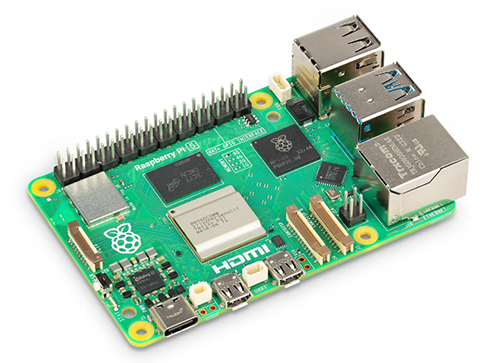
SC1112

Raspberry Pi

$79.61 - $86.40

IN STOCK 10293
Buy

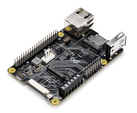
ASX00049

Arduino

* $39.41 - * $44.41

IN STOCK 3132
Buy

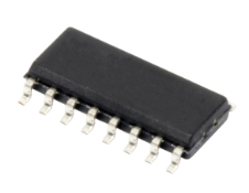
AD96685BRZ

Analog Devices Inc.

$1.72 - * $11.79

IN STOCK 4921
Buy

Reference Designs

RD006

Wurth Elektronik

RD006 - 3 W Dual-output isolated auxiliary supply for communication interfaces and measurement systems

CN0583

Analog Devices Inc.

Multistandard Micropower Verified Smoke Detection System-on-Module

Technical Resources

EVALUATION KITS

EVAL-AD7124-8SDZ

Analog Devices Inc.

$71.02 - * $75.98

IN STOCK 808
Buy
View All