ISL8088EVAL2Z
Renesas Electronics CorporationDC-DC Step Down 2 Non-Isolated Outputs ISL8088 Evaluation Board

ISL8225MEVAL4Z
Renesas Electronics CorporationEvaluation Board for ISL8225M Dual 15 A Single 30 A Step-Down Power Module


INA1620 Audio Operational Amplifier Evaluation Module
Texas InstrumentsINA1620 Audio Operational Amplifier Evaluation Module
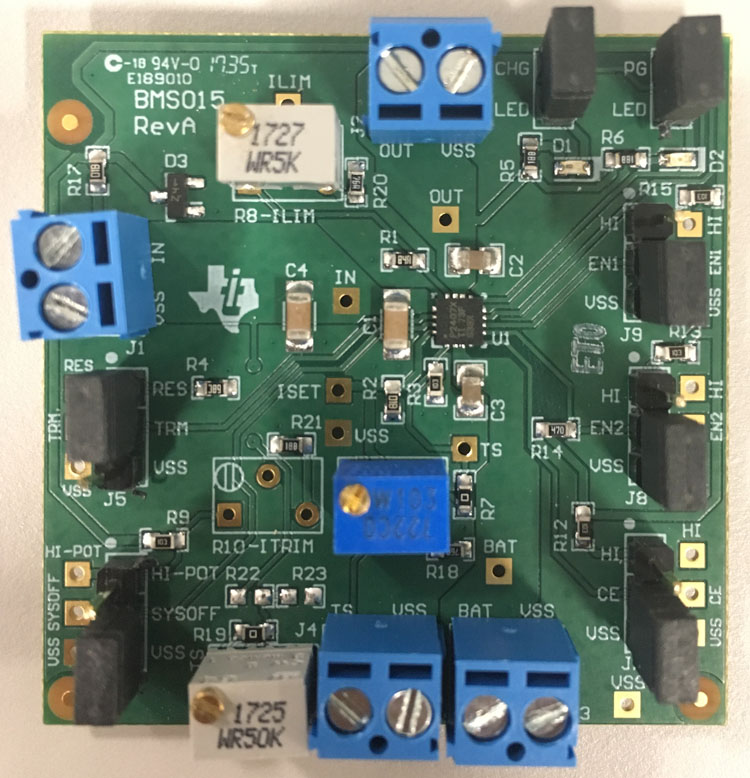
bq24078 1.5A Single-Chip Li-Ion and Li-Polymer Charger Management IC Evaluation Module
Texas Instrumentsbq24078 1.5A Single-Chip Li-Ion and Li-Polymer Charger Management IC Evaluation Module

Evaluation module for the ISO1212 dual-channel isolated digital input receiver
Texas InstrumentsEvaluation module for the ISO1212 dual-channel isolated digital input receiver
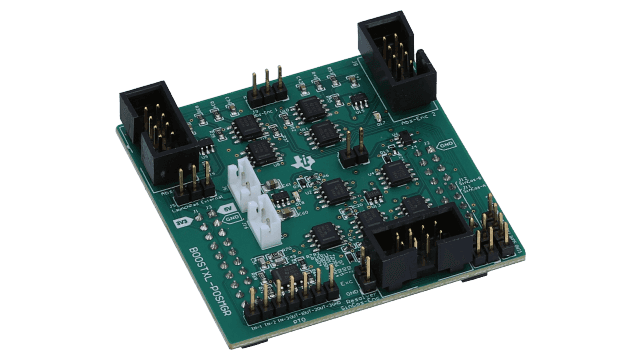
C2000 DesignDRIVE position manager BoosterPack™ plug-in module
Texas InstrumentsC2000 DesignDRIVE position manager BoosterPack™ plug-in module

ADP1864-EVALZ
Analog Devices Inc.The ADP1864 is a compact, inexpensive, constant-frequency current-mode step-down dc-to-dc controller. The ADP1864 drives a P-channel MOSFET that regulates an output voltage as low as 0.8 V with ?2% accuracy, for up to 5 A load currents, from input voltages as high as 14 V.The ADP1864 provides system flexibility by allowing accurate setting of the current limit with an external resistor, and the output voltage is easily adjustable using two external resistors. The ADP1864 includes an internal soft start to allow quick power-up while preventing input inrush current. Additional safety features include short-circuit protection, output overvoltage protection, and input undervoltage protection. Current-mode control provides fast and stable load transient performance, while the 580 kHz operating frequency allows a small inductor to be used in the system. To further the life of a battery source, the controller turns on the external P-channel MOSFET 100% of the duty cycle during dropout.The ADP1864 operates over the ?40?C to +125?C temperature range and is available in a small, low profile, 6-lead TSOT package.APPLICATIONS Wireless devices 1- to 3-cell Li-Ion battery-powered applications Set-top boxes Processor core power supplies Hard disk drives

ADP1870-1.0-EVALZ
Analog Devices Inc.The ADP1870 / ADP1871?are versatile current-mode, synchronous step-down controllers that provide superior transient response, optimal stability, and current-limit protection by using a constant on-time, pseudo-fixed frequency with a programmable current limit, current-control scheme. In addition, these devices offer optimum performance at low duty cycles by utilizing valley current-mode control architecture. This allows the ADP1870 / ADP1871 to drive all N-channel power stages to regulate output voltages as low as 0.6 V.The ADP1871 is the power saving mode (PSM) version of the device and is capable of pulse skipping to maintain output regulation while achieving improved system efficiency at light loads (see the Power Saving Mode (PSM) Version (ADP1871) section for more information).Available in three frequency options (300 kHz, 600 kHz, and 1.0 MHz, plus the PSM option), the ADP1870 / ADP1871 are well suited for a wide range of applications that require a single-input power supply range from 2.95 V to 20 V. Low voltage biasing is supplied via a 5 V internal LDO.In addition, an internally fixed soft start period is included to limit input in-rush current from the input supply during startup and to provide reverse current protection during soft start for a precharged output. The low-side current-sense, current-gain scheme and integration of a boost diode, along with the PSM/forced pulse width modulation (PWM) option, reduce the external part count and improve efficiency.The ADP1870 / ADP1871 operate over the -40?C to +125?C junction temperature range and are available in 10-lead MSOP package.

ADP197CP-EVALZ
Analog Devices Inc.The ADP197 is a high-side load switch designed for operation between 1.8 V and 5.5 V. This load switch provides power domain isolation, helping extended power domain isolation. The device contains a low on-resistance, N-channel MOSFET that supports more than 3 A of continuous current and minimizes power loss. The low 18 ?A quiescent current and ultralow shutdown current make the ADP197 ideal for battery-operated portable equipment. The built-in level shifter for enable logic makes the ADP197 compatible with many processors and GPIO controllers.Overtemperature protection circuitry activates if the junction temperature exceeds 125?C, thereby protecting itself and downstream circuits from potential damage.In addition to operating performance, the ADP197 occupies minimal printed circuit board (PCB) space with an area of less than 1.5 mm2 and a height of 0.60 mm.The ADP197 is available in an ultrasmall, 1 mm ? 1.5 mm, 6-ball, 0.5 mm pitch WLCSP.

ADP5061CB-EVALZ
Analog Devices Inc.The ADP5061 charger is fully compliant with USB 3.0 and the USB Battery Charging Specification 1.2 and enables charging via the mini USB VBUS pin from a wall charger, car charger, or USB host port.The ADP5061 operates from a 4 V to 6.7 V input voltage range but is tolerant of voltages up to 20 V. The 20 V voltage tolerance alleviates the concerns about the USB bus spiking during disconnect or connect scenarios.The ADP5061 features an internal FET between the linear charger output and the battery. This permits battery isolation and, hence, system powering under a dead battery or no batteryscenario, which allows for immediate system function on connection to a USB power supply.Based on the type of USB source, which is detected by an external USB detection chip, the ADP5061 can be set to apply the correct current limit for optimal charging and USB compliance.The ADP5061 has three factory programmable digital input/output pins that provide maximum flexibility for different systems. These digital input/output pins permit combinations of features such as, input current limits, charging enable and disable, charging current limits, and a dedicated interrupt output pin. APPLICATIONS Digital still cameras Digital video cameras Single cell Li-Ion portable equipment PDAs, audio, GPS devices Portable medical devices Mobile phones

ADP5310READJ-EVALZ
Analog Devices Inc.The ADP5310 combines dual buck regulators and one load switchin a 16-lead TSSOP_EP package that meets demanding performanceand board space requirements. The device enables directconnection to a wide input voltage range of 2.7 V to 15.0 V, allowingthe use of multiple alkaline/NiMH or lithium cells and otherpower sources.The buck regulator in Channel 1 uses a current mode, constantfrequency pulse-width modulation (PWM) control scheme forexcellent stability and transient performance, which provides upto 800 mA of output current. The automatic PWM/pulse skippingmode (PSM) control scheme achieves excellent efficiency in lightoutput current. A power-good signal indicates that the outputof Channel 1 is within 92% of its nominal value.An ultralow power buck regulator is integrated in Channel 2 withthe SYNC/MODE pin to control its operation mode. WhenSYNC/MODE is set to low, the buck regulator operates in hysteresismode, which draws only 700 nA of quiescent current to regulatethe output under zero load and provides up to 50 mA of outputcurrent. Hysteresis mode helps achieve excellent efficiency at lessthan 1 mW and can work as a keep-alive power supply in a batterypoweredsystem. When the SYNC/MODE pin is set to high, thebuck regulator switches to a traditional constant frequency PWMcontrol scheme to provide low output ripple for noise sensitiveapplications, and the buck regulator provides up to 300 mA ofoutput current in PWM mode.Channel 3 integrates a high-side load switch that operates from1.65 V to 5.5 V with its input connected to the output of Channel 2.The load switch provides power domain isolation and extendsbattery operation time.Other key safety features of the ADP5310 include overcurrentprotection (OCP), thermal shutdown (TSD), and input undervoltagelockout (UVLO). The ADP5310 is rated for the ?40?Cto +125?C junction temperature range.Applications Energy (gas and water) metering Portable and battery-powered equipment Medical applications? Keep-alive power supplies

ADP7104RD-EVALZ
Analog Devices Inc.The ADP7104 is a CMOS, low dropout linear regulator that operates from 3.3 V to 20 V and provides up to 500 mA of output current. This high input voltage LDO is ideal for regulation of high performance analog and mixed signal circuits operating from 19 V to 1.22 V rails. Using an advanced proprietary architecture, it provides high power supply rejection, low noise, and achieves excellent line and load transient response with just a small 1 ?F ceramic output capacitor.The ADP7104 is available in seven fixed output voltage options and an adjustable version, which allows output voltages that range from 1.22 V to VIN ? VDO via an external feedback divider.The ADP7104 output noise voltage is 15 ?V rms and is independent of the output voltage. A digital power-good output allows power system monitors to check the health of the output voltage. A user programmable precision undervoltage lockout function facilitates sequencing of multiple power supplies. The ADP7104 is available in 8-lead, 3 mm ? 3 mm LFCSP and 8-lead SOIC packages. The LFCSP offers a very compact solution and also provides excellent thermal performance for applications requiring up to 500 mA of output current in a small, low-profile footprint. APPLICATIONS Regulation to noise sensitive applications:?ADC, DAC circuits, precision amplifiers, high frequency oscillators, clocks, and PLLs Communications and infrastructure Medical and healthcare Industrial and instrumentation
ADP7104RDZ-REDYKIT
Analog Devices Inc.The ADP7104 is a CMOS, low dropout linear regulator that operates from 3.3 V to 20 V and provides up to 500 mA of output current. This high input voltage LDO is ideal for regulation of high performance analog and mixed signal circuits operating from 19 V to 1.22 V rails. Using an advanced proprietary architecture, it provides high power supply rejection, low noise, and achieves excellent line and load transient response with just a small 1 ?F ceramic output capacitor.The ADP7104 is available in seven fixed output voltage options and an adjustable version, which allows output voltages that range from 1.22 V to VIN ? VDO via an external feedback divider.The ADP7104 output noise voltage is 15 ?V rms and is independent of the output voltage. A digital power-good output allows power system monitors to check the health of the output voltage. A user programmable precision undervoltage lockout function facilitates sequencing of multiple power supplies. The ADP7104 is available in 8-lead, 3 mm ? 3 mm LFCSP and 8-lead SOIC packages. The LFCSP offers a very compact solution and also provides excellent thermal performance for applications requiring up to 500 mA of output current in a small, low-profile footprint. APPLICATIONS Regulation to noise sensitive applications:?ADC, DAC circuits, precision amplifiers, high frequency oscillators, clocks, and PLLs Communications and infrastructure Medical and healthcare Industrial and instrumentation

ADP7112CB-EVALZ
Analog Devices Inc.The ADP7112 is a CMOS, low dropout (LDO) linear regulator that operates from 2.7 V to 20 V and provides up to 200 mA of output current. This high input voltage LDO is ideal for the regulation of high performance analog and mixed signal circuits operating from 20 V down to 1.2 V rails. Using an advanced proprietary architecture, the device provides high power supply rejection, low noise, and achieves excellent line and load transient response with a small 2.2 ?F ceramic output capacitor. The ADP7112?regulator output noise is 11 ?V rms independent of the output voltage for the fixed options of 5 V or less.The ADP7112?is available in 16 fixed output voltage options. The following voltages are available from stock: 1.2 V (adjustable), 1.8 V, 2.5 V, 3.3 V, and 5.0 V. Additional voltages available by special order are 1.5 V, 1.85 V, 2.0 V, 2.2 V, 2.75 V, 2.8 V, 2.85 V, 3.8 V, 4.2 V, and 4.6 V.Each fixed output voltage can be adjusted above the initial set point with an external feedback divider. This allows the ADP7112?to provide an output voltage from 1.2 V to VIN ? VDO with high PSRR and low noise.User programmable soft start with an external capacitor is available in the?ADP7112. The ADP7112?is available in a 6-ball 1 mm ? 1.2mm WLCSP, making it a very compact solution.Applications Regulation to noise sensitive applications ADC, DAC circuits, precision amplifiers, power for VCO VTUNE control Communications and infrastructure Medical and healthcare Industrial and instrumentation

ADP7157CP-04-EVALZ
Analog Devices Inc.The ADP7157 is an adjustable linear regulator that operates from 2.3 V to 5.5 V and provides up to 1.2 A of output current. Output voltages from 1.2 V to 3.3 V are possible depending on the model. Using an advanced proprietary architecture, the device provides high power supply rejection and ultralow noise, achieving excellent line and load transient response with only a 10 ?F ceramicoutput capacitor.The ADP7157 is available in four models that optimize powerdissipation and PSRR performance as a function of the inputand output voltage.The typical output noise the ADP7157 regulator is 0.9 ?V rms from 100 Hz to 100 kHz and 1.7 nV/?Hz for noise spectral density from 10 kHz to 1 MHz. The ADP7157 is available in 10-lead, 3 mm ?3 mm LFCSP and 8-lead SOIC packages, making it not only avery compact solution, but also providing excellent thermalperformance for applications requiring up to 1.2 A of outputcurrent in a small, low profile footprint.Applications Regulation to noise sensitive applications: phase-locked loops (PLLs), voltage controlled oscillators (VCOs), and PLLs with integrated VCOs Communications and infrastructure Backhaul and microwave links

ADP7158CP-3.3EVALZ
Analog Devices Inc.The ADP7158 is a linear regulator that operates from 2.3 V to 5.5 V and provides up to 2 A of output current. Using an advanced proprietary architecture, it provides high power supply rejection and ultralow noise, achieving excellent line and load transient response with only a 10 ?F ceramic output capacitor.There are 16 standard output voltages for the ADP7158. The following voltages are available from stock: 1.2 V, 1.8 V, 2.0 V, 2.5 V, 2.8 V, 3.0 V, and 3.3 V. Additional voltages available by special order are 1.3 V, 1.5 V, 1.6 V, 2.2 V, 2.6 V, 2.7 V, 2.9 V, 3.1 V, and 3.2 V.The ADP7158 regulator typical output noise is 0.9 ?V rms from 100 Hz to 100 kHz and 1.7 nV/?Hz for noise spectral density from 10 kHz to 1 MHz. The ADP7158 is available in a 10-lead, 3 mm ? 3 mm LFCSP and 8-lead SOIC packages, making it not only a very compact solution, but also providing excellent thermal performance for applications requiring up to 2 A of output current in a small, low profile footprint.Applications Regulation to noise sensitive applications: phase-locked loops (PLLs), voltage controlled oscillators (VCOs), and PLLs with integrated VCOs Communications and infrastructure Backhaul and microwave links

ADRF5045-EVALZ
Analog Devices Inc.The ADRF5045 is a general-purpose, single-pole, four-throw (SP4T) switch manufactured using a silicon process. It comes in a 24-terminal land grid array (LGA) package and provides high isolation and low insertion loss from 9 kHz to 30 GHz.This broadband switch requires dual supply voltages, +3.3 V and ?3.3 V, and provides complementary metal-oxide semiconductor (CMOS)/low voltage transistor-transistor logic (LVTTL) logiccompatible control.Applications Test instrumentation Microwave radios and very small aperture terminals (VSATs) Military radios, radars, and electronic counter measures (ECMs) Broadband telecommunications systems

ADRF5141-EVALZ
Analog Devices Inc.The ADRF5141 is a reflective, single pole double-throw (SPDT) switch manufactured in the silicon process. It is used in transmit-receive (T/R) applications with an integrated power limiter at the receive side. The ADRF5141 operates from 8 GHz to 12 GHz. The RX arm with the integrated power limiter has a limiting capability of 18 dBm output power (TBC) with a low insertion loss of 1.3 dB at 10 GHz while the TX arm has an insertion loss of 0.9 dB at 10 GHz. The ADRF5141 draws a low current of 13 ?A on the positive supply of +3.3 V and 360 ?A on negative supply of ?3.3 V. The device employs complementary metal-oxide semiconductor (CMOS)-/low voltage transistor to transistor logic (LVTTL)-compatible controls. The ADRF5141 requires no additional driver circuitry, making it an ideal alternative to GaN and PIN diode-based switches. The ADRF5141 comes in a 20-lead, 3.0 mm ? 3.0 mm, RoHS-compliant, land grid array (LGA) package and can operate from ?40?C to +85?.APPLICATIONSElectronic warfareMilitary radios, radars, and electronic counter measuresGaN and PIN diode replacement


