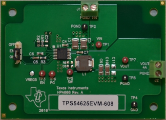
TPS54625 Synchronous Step-Down Converter Evaluation Module
Texas InstrumentsTPS54625 Synchronous Step-Down Converter Evaluation Module

ADS54RF63 12-Bit; 550-MSPS; RF Sampling Analog-to-Digital Converter Evaluation Module
Texas InstrumentsADS54RF63 12-Bit; 550-MSPS; RF Sampling Analog-to-Digital Converter Evaluation Module

TMP451 1.7-V remote and local temperature sensor evaluation module
Texas InstrumentsTMP451 1.7-V remote and local temperature sensor evaluation module
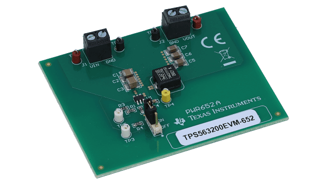
TPS563200 4.5V to 17V Input; 3A Synchronous Step Down Converter with Integrated FETs
Texas InstrumentsTPS563200 4.5V to 17V Input; 3A Synchronous Step Down Converter with Integrated FETs

Evaluation Module for TLV117125 1A; Positive Fixed Voltage; Low-Dropout Linear Regulator
Texas InstrumentsEvaluation Module for TLV117125 1A; Positive Fixed Voltage; Low-Dropout Linear Regulator

Synchronous Step-up DC DC Converter for White LED Applications
Texas InstrumentsSynchronous Step-up DC DC Converter for White LED Applications

SN65LVDS31-32EVM evaluation module for SNx5LVDS31 & SNx5LVDS32
Texas InstrumentsSN65LVDS31-32EVM evaluation module for SNx5LVDS31 & SNx5LVDS32

SHA-1/HMAC BASED SECURITY AND AUTHENTICATION IC
Texas InstrumentsSHA-1/HMAC BASED SECURITY AND AUTHENTICATION IC

Power-Distribution Switch with Adjustable Current-Limit Evaluation Module for TPS2553DRV1EVM-364
Texas InstrumentsPower-Distribution Switch with Adjustable Current-Limit Evaluation Module for TPS2553DRV1EVM-364


TPS54628 6-A Synchronous Step-Down Converter Evaluation Module
Texas InstrumentsTPS54628 6-A Synchronous Step-Down Converter Evaluation Module

DRV8308 evaluation module for three-phase brushless DC motor pre-drivers
Texas InstrumentsDRV8308 evaluation module for three-phase brushless DC motor pre-drivers

TS3A226AE evaluation module for autonomous audio-headset switch
Texas InstrumentsTS3A226AE evaluation module for autonomous audio-headset switch


