LM2852Y-2.5EVAL
Texas InstrumentsPower Management IC Development Tools 2A 500/1500kHz Synchronous SIMPLE SWITCH

STEVAL-SMARTAG1
STMicroelectronicsRF Development Tools NFC Dynamic Tag sensor node evaluation board
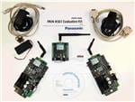
EVAL-PAN1740
Panasonic Industrial DevicesBluetooth Development Tools (802.15.1) PAN1740 EVALUATION KIT


AFE7444 quad-channel RF-sampling AFE with 14-bit 9-GSPS DAC and 3-GSPS ADC evaluation module
Texas InstrumentsAFE7444 quad-channel RF-sampling AFE with 14-bit 9-GSPS DAC and 3-GSPS ADC evaluation module
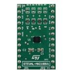
STEVAL-MKI189V1
STMicroelectronicsSockets & Adapters LSM6DSM adapter board for a standard DIL24 socket
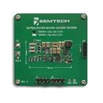
TSDMRX-19V-20W-EVM
Semtech CorporationPower Management IC Development Tools WP DUAL MODE RX UP TO 20W, 19V
EVAL-PAN1740
Panasonic Industrial DevicesBluetooth Development Tools (802.15.1) PAN1740 EVALUATION KIT
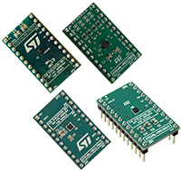
STEVAL-MKIT01V1 MEMS Sensor Sample Kit
STMicroelectronicsSTMicroelectronics' STEVAL-MKIT01V1 MEMS sensor sample kit includes a variety of MEMS sensor adapter boards and their corresponding software applications. Included in the kit are the LSM6DSL inertial module (STEVAL-MKI178V2), LIS2DW12 accelerometer (STEVAL-MKI179V1), LIS2MDL magnetometer (STEVAL-MKI181V1), and LPS22HB pressure sensor (STEVAL-MET001V1).
The included MEMS sensor adapter boards can be evaluated in stand-alone mode simply by connecting an I2C cable.
For a more in-depth evaluation, users can also order a motherboard based on the STM32F401VET6 microcontroller which functions as a bridge between the sensor adapter boards and a PC running STMicro's graphical user interface (GUI) or X-NUCLEO system board that is the standard ST evaluation tool.
Included MEMS Sensor Adapter Boards:
STEVAL-MKI178V2: LSM6DSL iNEMO inertial module with 3D accelerometer and 3D gyroscopes
STEVAL-MKI179V1: LIS2DW12 high-performance, ultra-low-power, 3-axis femto accelerometer
STEVAL-MKI181V1: LIS2MDL digital output magnetic sensor with an ultra-low-power, high-performance, 3-axis magnetometer
STEVAL-MET001V1: LPS22HB MEMS nano pressure sensor with a 260 hPa to 1260 hPa absolute digital output barometer
Included Software:
STSW-MEMS034: Unico Lite-source code
STSW-MKI109L: MEMS evaluation kit software package for Linux
STSW-MKI109M: MEMS evaluation kit software package for Mac OSX
STSW-MKI109W: MEMS evaluation kit software package for Windows

EVAL-AD7705EBZ
Analog Devices Inc.The AD7705 / AD7706?are complete analog front ends for low frequency measurement applications. These 2-/3-channel devices can accept low level input signals directly from a transducer and produce serial digital output. The devices employ a ?-? conversion technique to realize up to 16 bits of no missing codes performance. The selected input signal is applied to a proprietary, programmable-gain front end based around an analog modulator. The modulator output is processed by an on-chip digital filter. The first notch of this digital filter can be programmed via an on-chip control register, allowing adjustment of the filter cutoff and output update rate. The AD7705 / AD7706 devices operate from a single 2.7 V to 3.3 V or 4.75 V to 5.25 V supply. The AD7705 features two fully differential analog input channels; the AD7706 features three pseudo differential input channels. Both devices feature a differential reference input. Input signal ranges of 0 mV to 20 mV through 0 V to 2.5 V can be incorporated on both devices when operating with a VDD of 5 V and a reference of 2.5 V. They can also handle bipolar input signal ranges of ?20 mV through ?2.5 V, which are referenced to the AIN(?) inputs on the AD7705 and to the COMMON input on the AD7706.The AD7705 / AD7706 devices, with a 3 V supply and a 1.225 V reference, can handle unipolar input signal ranges of 0 mV to 10 mV through 0 V to 1.225 V. The devices can accept bipolar input ranges of ?10 mV through ?1.225 V. Therefore, the AD7705 / AD7706 devices perform all signal conditioning and conversion for a 2-channel or 3-channel system. The AD7705 / AD7706 are ideal for use in smart, microcontroller, or DSP-based systems. The devices feature a serial interface that can be configured for 3-wire operation. Gain settings, signal polarity, and update rate selection can be configured in software using the input serial port. The parts contains self-calibration and system calibration options to eliminate gain and offset errors on the part itself or in the system. CMOS construction ensures very low power dissipation, and the power-down mode reduces the standby power consumption to 20 ?W typ. These parts are available in a 16-lead, wide body (0.3 inch), plastic dual in-line package (DIP); a 16-lead, wide body (0.3 inch), standard small outline (SOIC) package; and a low profile, 16-lead, thin shrink small outline package (TSSOP).

ISL85005ADEMO1Z
Renesas Electronics CorporationPower Management IC Development Tools ISL85005A DEMO BOARD 1 - 12 LD DFN - RoH


