LTM4664 Demo Board | 48VIN, Single 50A μModule Regulator With Digital Power System Management
Analog Devices Inc.Demonstration circuit 2672A-B is a complete non-isolated 48V input, dual-phase single output, high efficiency, high density µModule regulator with 30V to 58V input range. The output can supply 50A maximum load current. The demo board has a LTM4664 µModule regulator, which is a dual 25A or single 50A step-down regulator with digital power system management. Please see LTM4664 datasheet for more detailed information.
DC2672A-B powers up to default settings and produces power based on configuration resistors without the need for any serial bus communication. This allows easy evaluation of the DC/DC converter. To fully explore the extensive power system management features of the part, download the GUI software LTpowerPlay™ onto your PC and use ADI’s I2C/SMBus/PMBus dongle DC1613A to connect to the board. LTpowerPlay allows the user to reconfigure the part on the fly and store the configuration in EEPROM, view telemetry of voltage, current, temperature and fault status.
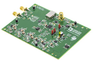
LTC2358-18, LT6658, ADA4522-2 Industrial Data Acquisition Nonisolated Board
Analog Devices Inc.Demonstration circuit 2677A is a reference design for robust industrial data acquisition applications for the LTC®2358-18. The LTC2358-18 is capable of high voltage measurements with a large input common range; however, the DC2677A implements input protection that allows up to 400V of continuous input protection. Combined with gas discharge tubes, which provide protection from surges, the DC2677A is capable of surviving extreme abuse.
This reference design includes the LTC2358-18 SAR ADC, ADA4522-2 dual zero-drift operational amplifier, and an LT6658 dual-output, high current reference for sensor
excitation.
The digital interface is an HSMC (high-speed mezzanine connector), which is compatible with Altera Cyclone V SoCkit and other Altera FPGA evaluation boards that support
3.3V CMOS I/O.
LTM4623EY Demo Board | 20VIN, 3A Step-Down µModule Regulator Configured as Inverting Output. –0.9VOUT to –5.2VOUT
Analog Devices Inc.Demonstration circuit 2721A-A features the LTM4623
µModule® regulator, a tiny high performance high efficiency
step-down regulator configured as an inverting
buck-boost regulator. The DC2721A-A has an operating
input voltage range of 4V to 15V and is able to provide
an output current of up to 2A. The output voltage can be
programmed between –0.6V and –5.5V. The LTM4623 is
a complete DC/DC point of load regulator in a thermally enhanced 6.25mm × 6.25mm × 1.82mm LGA package
requiring only a few input and output capacitors. The
LTM4623 data sheet must be read in conjunction with
this demo manual for working on or modifying demo circuit
2721A-A
DC2738A
Analog Devices Inc.The LTC7815 is a high performance triple output (buck/buck/boost) synchronous DC/DC switching regulator controller that drives all N-channel power MOSFET stages. Constant frequency current mode architecture allows a phase-lockable switching frequency of up to 2.25MHz. The LTC7815 operates from a wide 4.5V to 38V input supply range. When biased from the output of the boost converter or another auxiliary supply, the LTC7815 can operate from an input supply as low as 2.5V after start-up.The 28?A no-load quiescent current extends operating runtime in battery powered systems. OPTI-LOOP compensation allows the transient response to be optimized over a wide range of output capacitance and ESR values. The LTC7815 features a precision 0.8V reference for the bucks, 1.2V reference for the boost and a power good output indicator. The PLLIN/MODE pin selects among Burst Mode operation, pulse-skipping mode, or continuous inductor current mode at light loads.Applications Automotive Always-On and Start-Stop Systems Battery Operated Digital Devices Distributed DC Power Systems Multioutput Buck-Boost Applications
LT8365 Demo Board | Inverting Converter, 9V ≤ VIN ≤ 30V, -250VOUT @ up to 10mA
Analog Devices Inc.Demonstration circuit 2840A features the LT8365 in a Boost inverting configuration. It operates with a switching frequency of 400kHz and is designed to convert a 9V to 30V source to −250V, with 10mA output current.
The demo board contains an optional third charge pump stage for applications requiring higher output voltages. If needed, remove R14 and install optional components. Output voltage sensing connections remain the same.
The LT8365 can be used for different topologies with input voltages up to 60V. However, component selection in this demo circuit restrict the input voltage to 30V.
The demo board contains a selectable jumper, JP1, to aid in the selection of the desired Sync pin mode of operation. The default setting is Burst Mode® operation.
This layout is optimized for good EMI performance and small solution size. Input and output filters are necessary for CISPR 25 Class 5 emissions. Radiated emissions plots are included in this manual.
The data sheet gives a complete description of the device, operation and application information. The data sheet must be read in conjunction with this demo manual.
DC2884A
Analog Devices Inc.The LTC3108 is a highly integrated DC/DC converter ideal for harvesting and managing surplus energy from extremely low input voltage sources such as TEGs (thermoelectric generators), thermopiles and small solar cells. The step-up topology operates from input voltages as low as 20mV. The LTC3108 is functionally equivalent to the LTC3108-1 except for its unique fixed VOUT options.Using a small step-up transformer, the LTC3108 provides a complete power management solution for wireless sensing and data acquisition. The 2.2V LDO powers an external microprocessor, while the main output is programmed to one of four fixed voltages to power a wireless transmitter or sensors. The power good indicator signals that the main output voltage is within regulation. A second output can be enabled by the host. A storage capacitor provides power when the input voltage source is unavailable. Extremely low quiescent current and high efficiency design ensure the fastest possible charge times of the output reservoir capacitor.The LTC3108 is available in a small, thermally enhanced 12-lead (3mm ? 4mm) DFN package and a 16-lead SSOP?package. Output Voltage (Switcher) LTC3108 Selectable 2.35V, 3.3V, 4.1V or 5V LTC3108-1 Selectable 2.5V, 3V, 3.7V or 4.5V Applications Remote Sensors and Radio Power Surplus Heat Energy Harvesting HVAC Systems Industrial Wireless Sensing Automatic Metering Building Automation Predictive Maintenance
LT8551 Demo Board | High Power Boost Converter Based on the Phase Expander
Analog Devices Inc.Demonstration circuit 2896A-B demonstrates a high power boost converter and features the LT®8551 the phase expander with internal gate drivers. The DC2896A-B employs LTC3769, a single-phase boost controller as primary controller and LT8551 as the phase expander which added four more power phases. The increased number of power sections connected to the LT8551, results in greater higher level output power without a corresponding increase in the difficulty of the design or a sacrifice of primary controller LTC3769 features.
The input voltage range of DC2896A-B is from 10V to 46V and the output is 48V. The maximum input current is 12A per power section, so the maximum input current of DC2896A-B is 60A. It’s reflected to 30A of output current and output power of 1,440W at an input voltage of 24V. Correspondingly output current will drop to 14.5A and output power will to 720W at a 12V input voltage, to keep the input current at the same level of 60A. Both values will increase at higher voltages. The input current value can be increased above 60A, if heat sinks are installed, see parts list below.
The switching frequency is 250kHz and at a 24V input to 48VOUT at full load, the efficiency of DC2896A-B is 98%. As the input voltage decreases, the output current should be decreased as well, to prevent saturation of the DC2896A-B inductors, the derating curve presented on Figure 3. Efficiency curves presented on Figure 4.
DC2896A-B resistors R114 to R119 program the phase relationship between the power sections, by setting the Total Distinct Phase Number (TDPN). For increasing efficiency and reducing switching losses at light loads DC2896A-B supports disconnecting some power sections. This mode of operation designated as the stage shedding and it is programed by the jumper J3 STAGE SHED. Jumper JP1 programs the LT8551 SYNC pin and it allows DC2896A-B to be synchronized to an external clock. The print circuit board of DC2896A also supports two phase expander controllers, the LT8561 and LT8551, with versions DC2896A-A and DC2896A-B correspondingly. The table [1] in the electrical schematic describes differences between both versions, including controller biasing and gate drive voltages. DC2896A-B has jumper SHDN (JP2) for manually enable or disable controller. The SYNC (E19) input can be used to sync LT8551 with an external signal. There are also terminals that make it easy to monitor the control logic of the LT8551 functional. The current sense resistors RSNS1 to RSNS5 used for implementation of current mode control, monitoring and sharing current between the phases. To further increase efficiency DC2896A-B supports optional DCR sensing of inductors L1 to L5.
DC2896A-B includes sense line filters and filter options for inputs to the LT8551 in accordance with data sheet recommendations. Undervoltage shutdown, switching frequency and LT8551 ILIM current limit levels can all be adjusted by resistors or resistor jumpers. DC2896A-B comes with a housekeeping circuit based on U3 controller. It reduces the power dissipation that would otherwise occur at high input voltages in regulator transistor Q21. The housekeeping circuit also stabilizes converter biasing at sudden input voltage drops.
A high level of available output power without a corresponding high level of design complexity makes the LT8551 attractive for high power DC bus and battery systems in commercial, industrial and automotive settings. DC2896A-B features the LT8551EUKG in a thermally enhanced 52-pin 7mm × 8mm QFN package. The LT8551 and LTC3769 data sheets must be read in conjunction with this demo manual to properly use or modify DC2896A-B.
LTC1877EMS8 Demo Board | 2.65V to 10V Input, 1.5V to 3.3VOUT @ 600mA
Analog Devices Inc.Demonstration circuit DC290 is a constant-frequency step-down converter using an LTC1877 or an LTC1878 monolithic synchronous regulator. The LTC1878 has an input voltage range of 2.65V < VIN < 6V and the LTC1877 has an input voltage range of 2.65V < VIN < 10V. The LTC1878 is optimized for low voltage operation and is ideally suited for single Li-Ion cell or 3-NiCd/NiMH cell applications. The LTC1877, with its higher voltage capability, is ideally suited for two Li-Ion cells or 4- to 6-NiCd/NiMH cell applications.
LT8636 Demo Board | 42V, 5A Synchronous Step-Down Silent Switcher with 2.5μA Quiescent Current
Analog Devices Inc.Demonstration circuit 2918A is a 42V, 5A synchronous step-down SILENT SWITCHER with spread spectrum frequency modulation featuring the LT8636. The demo board is designed for 5V output from a 5.8V to 42V input. The wide input range allows a variety of input sources, such as automotive batteries and industrial supplies. The LT8636 is a compact, low emission, high efficiency, and high frequency synchronous monolithic step-down switching regulator. The proprietary silent switcher architecture minimizes electromagnetic emissions with simplified filter and reduced layout sensitivity. Selectable spread spectrum mode further improves EMI performance, making it perfect solution to the noise sensitive applications. The regulator’s ultralow 2.5μA quiescent current with the output in full regulation enables applications requiring highest efficiency at very light load currents, such as automotive and battery powered portable instruments.
Peak current mode control with minimum on-time of as small as 30ns allows high step-down conversion even at high frequency. The LT8636 switching frequency can be programmed either via oscillator resistor or external clock over a 200kHz to 3MHz range. The default frequency of demo circuit 2918A is 2MHz.
The SYNC/MODE pin on the demo board 2918A is grounded (JP1 at BURST position) by default for low ripple Burst Mode® operation. To synchronize to an external clock, move the Jump JP1 to SYNC/FCM and apply the external clock to the SYNC terminal on the 2918A. In sync mode, the part runs in forced continuous mode. Without external clock applied, the SYNC/MODE pin is floating, and the part runs in forced continuous mode. This mode offers fast transient response and full frequency operation over a wide load range. Alternatively, move the Jump JP1 to the SPREAD-SPECTRUM, and the SYNC/MODE is tied to INTVCC, the part runs in forced continuous mode with spread spectrum function enabled.
To get accurate efficiency measurement, measure the input voltage at the VIN_SENSE and GND terminals, which are Kelvin connected to the input cap C2 through signal traces.
The LT8636 is assembled in a 4mmx3mm LQFN package with exposed pads for low thermal resistance. The rated maximum load current is 5A, while derating is necessary for certain input voltage and thermal conditions.
The demo board has an EMI filter installed. The red line in Radiated EMI Performance is CISPR25 Class 5 peak limit. The circuit passes the test with a wide margin. To achieve EMI/EMC performance, the input EMI filter is required and the input voltage should be applied at VEMI terminal, and the setup can be referred to the CISPR 25 standards.
The LT8636 datasheet gives a complete description of the part, operation and application information. The datasheet must be read in conjunction with this demo manual for demo circuit 2918A. The layout recommendations for low EMI operation and best thermal performance are available in the datasheet section Low EMI PCB Layout and Thermal Considerations and Peak Output Current. Contact ADI applications engineer for support.
DC2922A-B
Analog Devices Inc.The LTC7802 is a high performance dual step-down synchronous DC/DC switching regulator controller that drives all N-channel power MOSFET stages. Constant frequencycurrent mode architecture allows a phase-lockable switching frequency of up to 3MHz. The LTC7802 operates from a wide 4.5V to 40V input supply range. Power loss and supply noise are minimized by operating the two controller output stages out-of-phase.The very low no-load quiescent current extends operating runtime in battery powered systems. OPTI-LOOP compensation allows the transient response to be optimizedover a wide range of output capacitance and ESR values. The LTC7802 features a precision 0.8V reference and power good output indicators. The MODE pin selects among Burst Mode operation, pulse-skipping mode, or continuous inductor current mode at light loads.The LTC7802 additionally features spread spectrum operation which significantly reduces the peak radiated and conducted noise on both the input and output supplies, making it easier to comply with electromagnetic interference (EMI) standards.APPLICATIONSAutomotive and TransportationIndustrialMilitary/Avionics
LTC4450 | 18V, 12A Low Quiescent Current Ideal Diode with Shutdown Mode
Analog Devices Inc.Demonstration Circuit 3001A-A showcases the LTC4450 ideal diode controller with an integrated low RDS(ON) MOSFET. The board includes two independent LTC4450 ideal diodes sharing a common ground and operates over a range of 0V to 18V, carrying up to 12A. The board can be set up in a diode-OR configuration by connecting the output channels together.
LT3001 Demo Board | Micropower No-Opto isolated Flyback Converter with 65V/1.2A Switch
Analog Devices Inc.Demonstration circuit 3006A is a compact no-opto
isolated flyback converter featuring the LT3001. The
DC3006A outputs 12V, and maintains tight regulation
with as load current from 1.5mA up to 300mA over an
input voltage from 4V to 32V. The output current capability increases with the input voltage, as shown in the
Performance Summary table.
Transformer leakage inductance causes a voltage spike on the primary side after the power switch turns off. The leakage inductance spike is limited within the MOSFET’s voltage rating of 65V with an RC snubber and a TVS clamp which damp the ringing and clamp the MOSFET drain voltage to a safe level.
The Performance Summary table summarizes the performance of the demo board at room temperature. The demo circuit can be easily modified for different applications with some pre-designed transformers.
The LT3001 datasheet gives a complete description of the part, operation and application information. The datasheet must be read in conjunction with this quick start guide for demo circuit 3006A.
LTM4693 | 2.6V - 5.5V Input to 1.8V - 5V Output, Ultrathin 2A Buck-Boost μModule Regulator
Analog Devices Inc.Demonstration circuit DC3016A is a buck-boost power supply featuring the LTM4693, ultrathin, highly efficient, 2A buck-boost μModule® regulator. The LTM4693 regulates an output voltage above, below, or equal to the input voltage. This demonstration circuit is designed to have an input voltage from 2.6V to 5.5V with selectable 1.8V, 2.5V, 3.3V, and 5V output voltage up to 2A load. Derating may be necessary for specific VIN, VOUT, and thermal conditions.
This demo board includes a mode selector that allows the converter to run in CCM or Burst Mode® operation. Synchronization to an external clock is also possible. The switching frequency can be adjusted from 1MHz to 4MHz by a resistor. And the soft-start period is programmable by an external capacitor. The LTM4693 data sheet gives a complete description of these functions, operation, and application information. The data sheet must be read in conjunction with this quick start guide for demo circuit 3016A.
DC3020A
Analog Devices Inc.The LT8636/LT8637 synchronous step-down regulator features Silent Switcher architecture designed to minimize EMI emissions while delivering high efficiency at high switching frequencies. Peak current mode control with a 30ns minimum on-time allows high step-down ratios even at high switching frequencies.The LT8636?s ultralow 2.5?A quiescent current?with the output in full regulation?enables applications requiring highest efficiency at very small load currents. The LT8637 has external compensation to enable current sharing and fast transient response at high switching frequencies. A CLKOUT pin enables synchronizing other regulators to the LT8636/LT8637.Burst Mode operation enables ultralow standby current consumption, forced continuous mode can control frequency harmonics across the entire output load range, or spread spectrum operation can further reduce EMI emissions. Soft-start and tracking functionality is accessed via the TR/SS pin, and an accurate input voltage UVLO threshold can be set using the EN/UV pin.APPLICATIONS Automotive and Industrial Supplies General Purpose Step-Down
LT4200 | 12V, 50A Hot Swap E-Fuse
Analog Devices Inc.Demonstration circuit 3024A showcases the LT4200 50A hot swap E-fuse with guaranteed SOA. Included on the board are input voltage dividers for undervoltage and overvoltage protection, LEDs to indicate input voltage, output voltage, fault and power bad conditions, and jumpers to enable auto retry and to select circuit breaker delay. Turrets are provided for monitoring input voltage, output voltage, output status, and most of the pins on the LT4200.
LTC3307B | 3.3V to 1.8V at 3A, 6.6MHz Low EMI Buck Regulator in a 0.47cm2 Solution
Analog Devices Inc.Demonstration circuit 3054A-A features the LTC3307B 5V, 3A synchronous step-down Silent Switcher® operating as a 6.6MHz, 3.3V to 1.8V 3A buck regulator. The LTC3307B supports adjustable output voltages from 0.5V to VIN, and operating frequencies from 3MHz up to 10MHz. The LTC3307B is a compact, ultralow emission, high efficiency, and high speed synchronous monolithic step-down switching regulator. A minimum on-time of 22ns enables high VIN to low VOUT conversion ratios at high switching frequencies.
The DC3054A-A operating mode may be selected as Burst Mode® operation, skip or forced continuous (FC) mode. Setting JP1 to the FC/SYNC position will allow the LTC3307B to sync to a clock frequency from 3MHz to 10MHz. The LTC3307B operates in forced continuous mode when syncing to an external clock. The DC3054A-A is set to a fixed 6.6MHz.
The DC3054A-A is set to a fixed 6.6MHz frequency by connecting RT to VIN through a 0Ω resistor, R9. The frequency can be easily changed by removing R9 and setting an appropriate resistor in the R4 location to obtain the desired frequency. Refer to the LTC3307B data sheet for the proper RT value for a desired switching frequency.
The LTC3307B data sheet gives a complete description of the device, operation and application information. The data sheet must be read in conjunction with the demo manual. The LTC3307B is assembled in a 2mm × 2mm LQFN package with exposed pads for low thermal resistance. The layout recommendations for low EMI operation and maximum thermal performance are available in the data sheet section Low EMI PCB Layout.
LT3002 Demo Board | Micropower No-Opto Isolated Flyback Converter with 65V/3.5A Switch
Analog Devices Inc.Demonstration circuit 3077A is a compact no-opto isolated flyback converter featuring the LT3002. The DC3077A outputs 12V and maintains tight regulation with a load current from 5mA up to 1.1A over an input voltage from 10V to 30V. The output current capability increases with the input voltage, as shown in the Performance Summary table.
Transformer leakage inductance causes a voltage spike on the primary side after the power switch turns off. The leakage inductance spike is limited within the MOSFET’s voltage rating of 65V with an RC snubber and a TVS clamp which damp the ringing and clamp the MOSFET drain voltage to a safe level.
The Performance Summary table summarizes the performance of the demo board at room temperature. The DC3077A demo circuit can be easily modified for different applications with some pre-designed transformers.
The LT3002 data sheet gives a complete description of the part, operation and application information. The data sheet must be read in conjunction with this quick start guide for demo circuit 3077A.
LTM4681 | PolyPhase Single Output Step-Down μModule Regulator with Digital PSM: 2 × LTM4681 at 240A
Analog Devices Inc.Demonstration circuit 3082A-A features the LTM4681: the wide input and output voltage range, high efficiency and power density, high current PolyPhase® single output DC/DC step-down μModule® regulator with digital power system management. DC3082A-A is configured as 8-phase single output using 2 × LTM4681. The factory default input voltage is 12V typical, output voltage is 1V at 240A typical or 250A peak with recommended 400LFM forced airflow. The demo board output voltages can be adjusted from 0.6V to 1V. Programming the output voltages to any value that is greater than 1V, requires derating output current based on thermal derating curves provided in the data sheet of the LTM4681. Heat sink or other appropriate electronic cooling systems can also be used in conjunction with forced airflow to further optimize the output power when the output is on and loaded with maximum output current. The factory default switching frequency is preset at 350kHz typical. DC3082A-A comes with PMBus interface and digital power system management functions. An onboard 12-pin connector is available for users to connect the dongle DC1613A to the demo board, provides an easy way to communicate and program the part using LTpowerPlay® software development tool. LTpowerPlay software and I2C/PMBus/SMBus dongle DC1613A allows users to monitor real time telemetry of input and output voltages, input and output current, switching frequency, internal IC die temperatures, power stage component temperatures and fault logs. Programmable parameters include device address, output voltages, control loop compensation, switching frequency, phase interleaving, DCM or CCM Mode of operation, digital soft-start, sequencing, and time based shutdown, fault responses to input and output overvoltage, output overcurrent, IC die and power component overtemperatures.
The LTM4681 is available in a thermally enhanced, low profile 330-Lead (15mm × 22mm × 8.17mm) BGA package. It is recommended to read the data sheet and demo manual of LTM4681 prior to using or making any hardware changes to DC3082A-A.
LTpowerPlay software can be downloaded here.
USB to PMBus Controller Dongle DC1613A for use with LTpowerPlay is available here.
DC309A
Analog Devices Inc.The LTC1773 is a current mode synchronous buck regulator controller that drives external complementary power MOSFETs using a fixed frequency architecture. The operating supply range is from 2.65V to 8.5V, making it suitable for 1- or 2-cell lithium-ion battery powered applications. Burst Mode? operation provides high efficiency at low load currents. 100% duty cycle provides low dropout operation which extends operating time in battery-operated systems.The operating frequency is internally set at 550kHz, allowing the use of small surface mount inductors. For switching-noise sensitive applications, it can be synchronized up to 750kHz. Peak current limit is user programmable with an external high side sense resistor. A SYNC/FCB control pin guarantees regulation of secondary windings regardless of load on the main output by forcing continuous operation. Burst Mode operation is inhibited during synchronization or when the SYNC/FCB pin is pulled low to reduce noise and RF interference. Soft-start is provided by an external capacitor.Synchronous rectification increases efficiency and eliminates the need for a Schottky diode, saving components and board space. The LTC1773 comes in a 10-lead MSOP package.Applications Cellular Telephones RF PA Supply Portable Instruments Wireless MODEMS Distributed Power Systems Notebook and Palm Top Computers, PDAs Single and Dual Cell Lithium-Ion Powered Devices
DC3110A
Analog Devices Inc.The ADBMS6816 is a multicell battery stack monitor that measures up to six series connected battery cells with a lifetime total measurement error (TME) of less than 1.5 mV. The cell measurement range of 0 V to 5 V makes the ADBMS6816 suitable for most battery chemistries. All six cells can be measured in 304 ?s, and lower data acquisition rates can be selected for high noise reduction.Multiple ADBMS6816 devices can be connected in series, permitting simultaneous cell monitoring of long, high voltage battery strings. Each ADBMS6816 has an isoSPI? interface for high speed, RF immune, long distance communications.Multiple devices are connected in a daisy chain with one host processor connection for all devices. This daisy chain can be operated bidirectionally, ensuring communication integrity even in the event of a fault along the communication path.The ADBMS6816 can be powered directly from the battery stack or from an isolated supply. The ADBMS6816 includes passive balancing for each cell, with individual pulse-width modulation (PWM) duty cycle control for each cell. Other features include an on-board 5 V regulator, seven general-purpose input/output (GPIO) lines, and a sleep state, where current consumption is reduced to 5.5 ?A.APPLICATIONS Electric and hybrid electric vehicles Backup battery systems Grid energy storage High power portable equipment


