
DC2422A-C
Analog Devices Inc.The LTC7812 is a high performance synchronous Boost+Buck DC/DC switching regulator controller that drives all N-channel power MOSFET stages. It contains independent step-up (boost) and step-down (buck) controllers that can regulate two separate outputs or be cascaded to regulate an output voltage from an input voltage that can be above, below or equal to the output voltage. The LTC7812 operates from a wide 4.5V to 38V input supply range. When biased from the output of the boost regulator, the LTC7812 can operate from an input supply as low as 2.5V after start-up. The 33?A no-load quiescent current extends operating run time in battery-powered systems.Unlike conventional buck-boost regulators, the LTC7812?s cascaded Boost+Buck solution has continuous, nonpulsating, input and output currents, substantially reducing voltage ripple and EMI. The LTC7812 has independent feedback and compensation points for the boost and buck regulation loops, enabling a fast output transient response that can be easily optimized externally.Applications Automotive and Industrial Power Systems High Power Battery Operated Systems

DC2429A
Analog Devices Inc.The LT3042 is a high performance low dropout linear regulator featuring LTC?s ultralow noise and ultrahigh PSRR architecture for powering noise sensitive RF applications. Designed as a precision current reference followed by a high performance voltage buffer, the LT3042 can be easily paralleled to further reduce noise, increase output current and spread heat on the PCB.The device supplies 200mA at a typical 350mV dropout voltage. Operating quiescent current is nominally 2mA and drops to
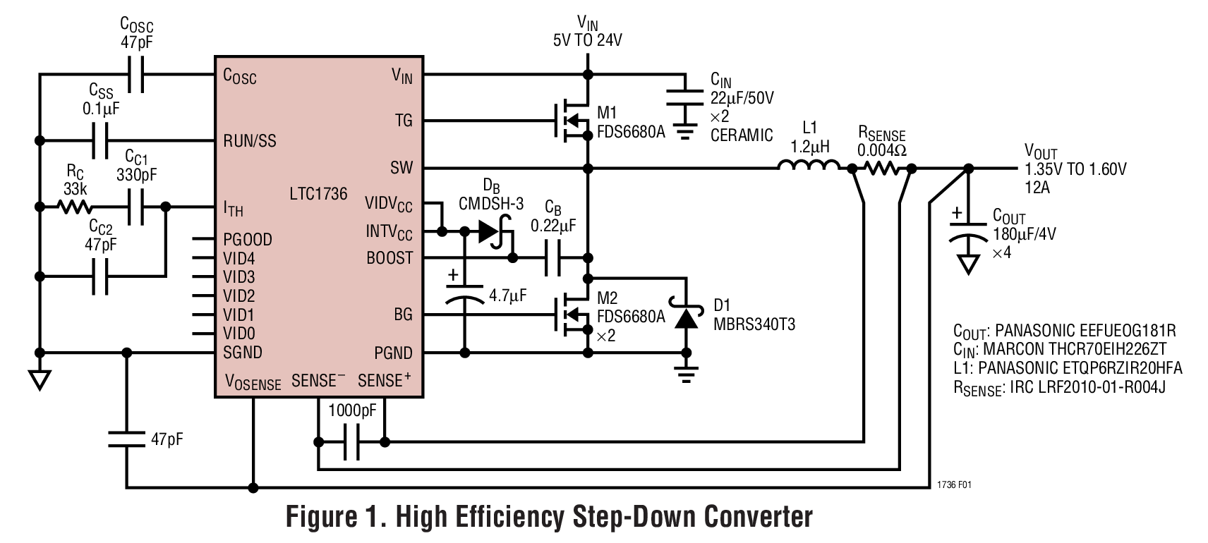
LTC1736CG | 5 Bit, VID CPU Power Converter, VIN = 5V to 24V, VOUT = 0.9V to 2.0V @ 12A
Analog Devices Inc.DC252A: Demo Board for the LTC1736 5-Bit Adjustable High Efficiency Synchronous Step-Down Switching Regulator.

DC2593A
Analog Devices Inc.The LT3045-1 is a high performance low dropout linear regulator featuring LTC?s ultralow noise and ultrahigh PSRR architecture for powering noise sensitive applications. Designed as a precision current reference followed by a high performance voltage buffer, the LT3045-1 can be easily paralleled to further reduce noise, increase output current and spread heat on the PCB. In addition to the LT3045 feature set, the LT3045-1 incorporates a VIOC tracking function to control an upstream switching converter to maintain a constant voltage across the LT3045-1 and hence minimize power dissipation.The device supplies 500mA at a typical 260mV dropout voltage. Operating quiescent current is nominally 2.3mA and drops to

DC2595A
Analog Devices Inc.The LTC3889 is a dual PolyPhase DC/DC synchronous step-down switching regulator controller with I2C-based PMBus compliant serial interface. This controller employs a constant-frequency, current-mode architecture, with high voltage input and output capability along with programmable loop compensation. The LTC3889 is supported by the LTpowerPlay? software development tool with graphical user interface (GUI).The EXTVCC pin supports voltages up to 14V allowing for optimized circuit efficiency and die temperature, and for the controller output to supply the chip power. Switching frequency, output voltage, and device address can be programmed both by digital interface as well as external configuration resistors. Parameters can be set via the digital interface or stored in EEPROM. Both outputs have an independent power good indicator and FAULT function.The LTC3889 can be configured for discontinuous (pulse-skipping) mode or continuous inductor current mode.APPLICATIONS Telecom, Datacom, and Storage Systems Industrial and Point of Load Applications

LT8708 80V VIN and VOUT Synchronous 4-Switch Buck-Boost DC/DC Controller with Flexible Bidirectional Capability
Analog Devices Inc.Demonstration circuit 2596A is a high performance bidirectional buck-boost converter featuring the LT®8708 that can operate from input voltages above, below or equal to the output voltage. The demo board input range is 36V to 75V. The output voltage is set at 48V and the output current limit at 6A.
The controller has integrated input voltage and output voltage regulators and two sets of input and output current regulators that control current flow in forward or reverse direction. Features are included that simplify bidirectional power conversion in battery/capacitor backup systems and other applications that may need regulation of VIN, VOUT, IIN and/or IOUT.
While the current mode control limits the inductor current both in normal and in reverse direction these current limits have some variation as input/output voltage changes. The forward and reverse input and output current regulators offer four accurate current limits that can be set individually.
The input voltage regulator is often used in applications with high impedance power sources and will reduce the forward current if the input voltage drops below the set
point. When operating with reverse current flow the input voltage regulator regulates the voltage at the input side.
The operating mode of the controller is determined through the MODE pin (jumper JP7 Pins 5 to 12) and can be set to discontinuous mode, hybrid discontinuous mode, forced continuous mode and Burst Mode® Operation.
The LT8708 is capable of bidirectional operation when operating in the continuous conduction mode (CCM). DCM, HCM and Burst Mode operation only allow power to flow in one direction. Additional circuitry may be needed depending on the application.
By feeding the LT8708 from a separate low voltage supply the power dissipation can be reduced. The LT8708 will start when >5.5V voltage is applied at the input (VIN pin), and when it is running it will draw current from the EXTVCC pin if the voltage at the pin is > 6.4V.
Typical efficiency with 5A load is above 96.3% across a 36V to 75V input range.
The LT8708 data sheet gives a complete description of the part, operation and application information. The data sheet should be read in conjunction with this quick start guide for DC2596A. The input voltage range of the LT8708 itself is 2.8V (need EXTVCC > 6.4V) to 80V and the output range is 1.3V to 80V.
The LT8708EUHG is assembled in a 40-Lead (5mm × 7mm) plastic QFN package with a thermal pad underneath the chip. Proper board layout is essential for maximum
thermal and electrical performance. See the data sheet Circuit Board Layout Checklist section.

LT8390A Demo Board | VIN = 4V to 24V, (60V Transient) with VOUT = 12V at 4A @ 2MHz
Analog Devices Inc.Demonstration circuit 2598A is a 60V 2MHz synchronous buck-boost controller featuring the LT8390A. It accepts an input voltage from 4V to 24V (with transient to 60V) and regulates 12V output at up to 4A. DC2598A features high efficiency and 2MHz switching frequency, a high speed for a 4-switch buck-boost controller. It has a PGOOD flag, short-circuit fault protection, ISMON current-monitoring output signal, and spread spectrum frequency modulation (SSFM) or frequency synchronization.

Starter Kit for LTC2986-1 | LTC2986-1 Motherboard (DC2618) + 20-Input Breakout Board (DC2210) + Linduino One (DC2026)
Analog Devices Inc.The DC2608 is the starter kit for demonstrating the performance and ease of use of the LTC2986-1, which is a complete temperature measurement system on a chip. This kit includes the DC2618 (main demo circuit containing the LTC2986-1) and the DC2210 (a simple experiment circuit allowing bread boarding). In addition to the starter demonstration kit, sensor specific demonstration boards highlighting the performance of RTDs, thermistors, or thermocouples are also available.

DC2615A
Analog Devices Inc.The LTC7151S is a high efficiency monolithic synchronous buck regulator capable of delivering 15A to the load. It uses a phase lockable controlled on-time constant frequency, current mode architecture. PolyPhase operation allows multiple LTC7151S regulators to run out-of-phase, which reduces the amount of input and output capacitors required. The operating supply voltage range is from 3.1V to 20V.The operating frequency is programmable from 400kHz to 3MHz with an external resistor. The high frequency capability allows the use of physically smaller inductor and capacitor sizes. For switching noise sensitive applications, the LTC7151S can be externally synchronized from 400kHz to 3MHz. The PHMODE pin allows the user control of the phase of the outgoing clock signal. The unique constant frequency/controlled on-time architecture is ideal for high step-down ratio applications that operate at high frequencies while demanding fast transient response. The LTC7151S uses second generation Silent Switcher 2 technology including integrated bypass capacitors to deliver a highly efficient solution at high frequencies with excellent EMI performance.Applications Automotive and Industrial Power Supplies Server Power Applications Distributed Power Systems Point-of-Load Supply for ASIC, FPGA, DSP, ?P, etc.

DC261A-A
Analog Devices Inc.The LT1795 is a dual current feedback amplifier with high output current and excellent large signal characteristics. The combination of high slew rate, 500mA output drive and up to ?15V operation enables the device to deliver significant power at frequencies in the 1MHz to 2MHz range. Short-circuit protection and thermal shutdown insure the device?s ruggedness. The LT1795 is stable with large capacitive loads and can easily supply the large currents required by the capacitive loading. A shutdown feature switches the device into a high impedance, low current mode, reducing power dissipation when the device is not in use. For lower bandwidth applications, the supply current can be reduced with a single external resistor.The LT1795 comes in the very small, thermally enhanced, 20-lead TSSOP package for maximum port density in line driver applications.Applications ADSL HDSL2, G.lite Drivers Buffers Test Equipment Amplifiers Video Amplifiers Cable Drivers

DC2620A-A
Analog Devices Inc.The LTC7106 is a precision, PMBus controlled, bidirectional current digital-to-analog converter that adjusts the output voltage of any conventional VFB referenced regulator. The LTC7106 can work with the vast majority of power management controllers or regulators to enable digital control of the output voltage. Internal power-on reset circuitry keeps the DAC output current at zero (high impedance IDAC) until a valid write takes place. Features include a range bit for easy interfacing to almost any impedance resistor divider, and an open-drain GPO output for controlling the Run or Enable pin of the DC/DC regulator. For most applications, the current DAC error is significantly attenuated with proper design. See more detail about VOUT accuracy in the Applications Information section of this data sheet. The LTC7106 is supported by the ADI LTpowerPlay? development tool with graphical user interface (GUI).Applications General Purpose Power Systems Telecom Systems Industrial Applications

DC2642A-B
Analog Devices Inc.The LTC4041 is a complete supercapacitor backup system for 2.9V to 5.5V supply rails. It contains a high current step-down DC/DC converter to charge a single supercapacitor or two supercapacitors in series. When input power is unavailable, the step-down regulator operates in reverse as a step-up regulator to backup the systemoutput from the supercapacitor(s).The LTC4041?s adjustable input current limit function reduces charge current to protect the input supply from overload while an external disconnect switch isolates theinput supply during backup. When the input supply drops below the adjustable PFI threshold, the 2.5A boost regulator delivers power from the supercapacitor to the systemoutput.An optional input overvoltage protection (OVP) circuit protects the LTC4041 from high voltage damage at the VIN pin. An internal supercapacitor balancing circuit maintainsequal voltages across each supercapacitor and limits the maximum voltage of each supercapacitor to a pre-determined value. The LTC4041 is available in a low profile (0.75mm) 24-Lead 4mm ? 5mm QFN package.ApplicationsRide-Through ?Dying Gasp? SuppliesHigh Current Ride-Through 3V to 5V UPSPower Meters/Industrial AlarmsServers/Solid State Drives

DC2645A
Analog Devices Inc.The LTC5594 is a direct conversion quadrature demodulator optimized for high linearity zero-IF and low-IF receiver applications in the 300MHz to 9GHz frequency range. The very wide IF bandwidth of more than 1GHz makes the LTC5594 particularly suited for demodulation of very wideband signals, especially in 5G front-haul/back-haul receiver applications. The outstanding dynamic range of the LTC5594 makes the device suitable for demanding infrastructure direct conversion applications. Proprietary technology inside the LTC5594 provides the capability to optimize OIP2 to 65dBm, and achieve image rejection better than 60dB. The DC offset control function allows nulling of the DC offset at the A/D converter input, thereby optimizing the dynamic range of true zero-IF receivers that use DC-coupled IF signal paths. The wideband RF and LO input ports make it possible to cover all the major wireless infrastructure frequency bands using a single device. The IF outputs of the LTC5594 are designed to interface directly with most common A/D converter input interfaces. The high OIP3 and high conversion gain of the device eliminate the need for additional amplifiers in the IF signal path.APPLICATIONS 5G Base Station Front-haul/Back-haul Receivers Military and Satellite Receivers Point-to-Point Broadband Radios High Linearity Direct Conversion I/Q SDR Test Instrumentation DPD Receivers

DC2658A
Analog Devices Inc.The LT8640S/LT8643S synchronous step-down regulator?features second generation Silent Switcher architecture designed to minimize EMI emissions while delivering high?efficiency at high switching frequencies. This includes the integration of bypass capacitors to optimize all the?fast current loops inside and make it easy to achieve?advertised EMI performance by reducing layout sensitivity.?This performance makes the LT8640S/LT8643S ideal for?noise-sensitive applications and environments.Peak current mode control with a 30ns minimum on-time?allows high step-down ratios even at high switching frequencies. The LT8643S has external compensation to?enable current sharing and fast transient response at high?switching frequencies.Burst Mode operation enables ultralow standby current?consumption, forced continuous mode can control frequency?harmonics across the entire output load range, or spread?spectrum operation can further reduce EMI emissions.APPLICATIONS Automotive and Industrial Supplies General Purpose Step-Down

LTM4664 Demo Board | 48VIN, Single 50A μModule Regulator With Digital Power System Management
Analog Devices Inc.Demonstration circuit 2672A-B is a complete non-isolated 48V input, dual-phase single output, high efficiency, high density µModule regulator with 30V to 58V input range. The output can supply 50A maximum load current. The demo board has a LTM4664 µModule regulator, which is a dual 25A or single 50A step-down regulator with digital power system management. Please see LTM4664 datasheet for more detailed information.
DC2672A-B powers up to default settings and produces power based on configuration resistors without the need for any serial bus communication. This allows easy evaluation of the DC/DC converter. To fully explore the extensive power system management features of the part, download the GUI software LTpowerPlay™ onto your PC and use ADI’s I2C/SMBus/PMBus dongle DC1613A to connect to the board. LTpowerPlay allows the user to reconfigure the part on the fly and store the configuration in EEPROM, view telemetry of voltage, current, temperature and fault status.

LTC2358-18, LT6658, ADA4522-2 Industrial Data Acquisition Nonisolated Board
Analog Devices Inc.Demonstration circuit 2677A is a reference design for robust industrial data acquisition applications for the LTC®2358-18. The LTC2358-18 is capable of high voltage measurements with a large input common range; however, the DC2677A implements input protection that allows up to 400V of continuous input protection. Combined with gas discharge tubes, which provide protection from surges, the DC2677A is capable of surviving extreme abuse.
This reference design includes the LTC2358-18 SAR ADC, ADA4522-2 dual zero-drift operational amplifier, and an LT6658 dual-output, high current reference for sensor
excitation.
The digital interface is an HSMC (high-speed mezzanine connector), which is compatible with Altera Cyclone V SoCkit and other Altera FPGA evaluation boards that support
3.3V CMOS I/O.

LTM4623EY Demo Board | 20VIN, 3A Step-Down µModule Regulator Configured as Inverting Output. –0.9VOUT to –5.2VOUT
Analog Devices Inc.Demonstration circuit 2721A-A features the LTM4623
µModule® regulator, a tiny high performance high efficiency
step-down regulator configured as an inverting
buck-boost regulator. The DC2721A-A has an operating
input voltage range of 4V to 15V and is able to provide
an output current of up to 2A. The output voltage can be
programmed between –0.6V and –5.5V. The LTM4623 is
a complete DC/DC point of load regulator in a thermally enhanced 6.25mm × 6.25mm × 1.82mm LGA package
requiring only a few input and output capacitors. The
LTM4623 data sheet must be read in conjunction with
this demo manual for working on or modifying demo circuit
2721A-A

DC2738A
Analog Devices Inc.The LTC7815 is a high performance triple output (buck/buck/boost) synchronous DC/DC switching regulator controller that drives all N-channel power MOSFET stages. Constant frequency current mode architecture allows a phase-lockable switching frequency of up to 2.25MHz. The LTC7815 operates from a wide 4.5V to 38V input supply range. When biased from the output of the boost converter or another auxiliary supply, the LTC7815 can operate from an input supply as low as 2.5V after start-up.The 28?A no-load quiescent current extends operating runtime in battery powered systems. OPTI-LOOP compensation allows the transient response to be optimized over a wide range of output capacitance and ESR values. The LTC7815 features a precision 0.8V reference for the bucks, 1.2V reference for the boost and a power good output indicator. The PLLIN/MODE pin selects among Burst Mode operation, pulse-skipping mode, or continuous inductor current mode at light loads.Applications Automotive Always-On and Start-Stop Systems Battery Operated Digital Devices Distributed DC Power Systems Multioutput Buck-Boost Applications

LT8365 Demo Board | Inverting Converter, 9V ≤ VIN ≤ 30V, -250VOUT @ up to 10mA
Analog Devices Inc.Demonstration circuit 2840A features the LT8365 in a Boost inverting configuration. It operates with a switching frequency of 400kHz and is designed to convert a 9V to 30V source to −250V, with 10mA output current.
The demo board contains an optional third charge pump stage for applications requiring higher output voltages. If needed, remove R14 and install optional components. Output voltage sensing connections remain the same.
The LT8365 can be used for different topologies with input voltages up to 60V. However, component selection in this demo circuit restrict the input voltage to 30V.
The demo board contains a selectable jumper, JP1, to aid in the selection of the desired Sync pin mode of operation. The default setting is Burst Mode® operation.
This layout is optimized for good EMI performance and small solution size. Input and output filters are necessary for CISPR 25 Class 5 emissions. Radiated emissions plots are included in this manual.
The data sheet gives a complete description of the device, operation and application information. The data sheet must be read in conjunction with this demo manual.

DC2884A
Analog Devices Inc.The LTC3108 is a highly integrated DC/DC converter ideal for harvesting and managing surplus energy from extremely low input voltage sources such as TEGs (thermoelectric generators), thermopiles and small solar cells. The step-up topology operates from input voltages as low as 20mV. The LTC3108 is functionally equivalent to the LTC3108-1 except for its unique fixed VOUT options.Using a small step-up transformer, the LTC3108 provides a complete power management solution for wireless sensing and data acquisition. The 2.2V LDO powers an external microprocessor, while the main output is programmed to one of four fixed voltages to power a wireless transmitter or sensors. The power good indicator signals that the main output voltage is within regulation. A second output can be enabled by the host. A storage capacitor provides power when the input voltage source is unavailable. Extremely low quiescent current and high efficiency design ensure the fastest possible charge times of the output reservoir capacitor.The LTC3108 is available in a small, thermally enhanced 12-lead (3mm ? 4mm) DFN package and a 16-lead SSOP?package. Output Voltage (Switcher) LTC3108 Selectable 2.35V, 3.3V, 4.1V or 5V LTC3108-1 Selectable 2.5V, 3V, 3.7V or 4.5V Applications Remote Sensors and Radio Power Surplus Heat Energy Harvesting HVAC Systems Industrial Wireless Sensing Automatic Metering Building Automation Predictive Maintenance


