5 kV rms Signal and Power Isolated CAN Transceiver forCAN FD Arduino Shield
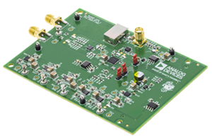
Analog Devices Inc.EVAL-ADM3055E-ARDZ is an Arduino Uno compatible Shield for an isolated controller area network with flexible data rate (CAN FD) communications port. The circuit interfaces to the local development platform via Serial Peripheral Interface (SPI) providing a simple method to add field bus communication to new and existing designs. EVAL-ADM3055E-ARDZ enables both the higher bandwidth CAN FD data rates (up to 8Mbps) demanded by modern multi-node CAN FD networks and the rugged electromagnetic compatibility (EMC) performance required by industrial environments.
The circuit uses the integrated auxiliary isolated digital channel of the ADM3055E transceiver for runtime configuration of the bus termination. The switchable termination circuitry connects a 120 Ω split termination with common-mode filtering capacitor between the CAN FD bus lines. Switchable termination allows on-the-fly software configuration of termination locations when the CAN FD bus is physically altered. Using switchable termination, each node can be used at any physical location without mechanical changes to the nodes and software can track the position of terminations in the network.
Additionally, the circuit can be set by the development platform to a reduced power standby state. While in the standby state, the isolated CAN FD communications port will notify the development platform of a remote wake-up request being transmitted by a remote CAN FD node to the CAN FD bus.
With the ADM3055E CAN FD transceiver, the circuit provides reinforced signal and power isolation between the node and CAN FD bus. Electrical connection to the CAN FD bus may be made either by screw terminal or the CAN CiA 303-1 male 9-pin sub-D port. Because the ADM3055E transceiver has an integrated isolated dc-to-dc converter, it does not require external power to be present on the CAN FD bus. The examples focus on CAN FD networks however this circuit is backwards compatible with classical CAN networks.
EVAL-ADM3056EEBZ
Analog Devices Inc.The ADM3056E is a 5.7 kV rms isolated controller area network (CAN) physical layer transceiver. The ADM3056E fully meets the CAN-FD ISO 11898-2: 2016 requirements and is further capable of supporting data rates as high as 12 Mbps.The device employs Analog Devices, Inc., iCoupler? technology to combine a highly robust 3-channel isolator and a CAN transceiver into a single SOIC, surface-mount package. The ADM3056E provides galvanic isolation between the CAN controller and physical layer bus.Safety and regulatory approvals (pending) for 5.7 kV rms isolation withstand voltage, 849 VPEAK working insulation voltage, 8 kV surge, and 8.3 mm creepage and clearance, ensure that the ADM3056E meets isolation requirements for high voltage applications.Low propagation delays through the isolation support longer bus cables. Slope control mode is available for standard CAN atlow data rates. Standby mode can minimize power consumption when the bus is idle, or if the node goes offline. Silent modeallows the TXD input to be ignored for listen only functionality.Dominant timeout functionality protects against bus lock-up in a fault condition, and current limiting and thermal shutdown features protect against output short circuits. The device is fully specified over the ?40?C to +125?C industrial temperature range and is available in a 16-lead, increased creepage, wide-body SOIC package.Applications CANOpen, DeviceNet, and other CAN bus implementations Solar inverters and battery management Motor and process control Industrial automation Transport and infrastructure
EVAL-ADM3058EEBZ
Analog Devices Inc.The ADM3058E is a 5.7 kV rms isolated controller area network (CAN) physical layer transceiver with a high perfor-mance, basic feature set. The ADM3058E fully meets the CAN flexible data rate (CAN FD) ISO 11898-2:2016 requirements and is further capable of supporting data rates as high as 12 Mbps.The device employs Analog Devices, Inc., iCoupler? technology to combine a 2-channel isolator and a CAN transceiver into a single small outline integrated circuit (SOIC) surface-mount package. The ADM3058E is a fully isolated solution for CAN and CAN FD applications. The ADM3058E provides isolation between the CAN controller and physical layer bus. Safety and regulatory approvals (pending) for a 5.7 kV rms withstand voltage and a 1500 V peak working voltage ensure that the ADM3058E meets application isolation requirements.Low loop propagation delays and the extended common-mode range of ?25 V support robust communication on longer bus cables. Dominant timeout functionality protects against bus lock up in a fault condition, and current limiting and thermal shutdown features protect against output short circuits. The CAN bus input and output pins are protected to ?40 V against accidental connection to a +24 V bus supply. The device is fully specified over the ?40?C to +125?C industrial temperature range.ApplicationsCANOpen, DeviceNet, and other CAN bus implementationsIndustrial automationProcess control and building controlTransport and infrastructure
EVAL-ADM3064EEBZ
Analog Devices Inc.The ADM3061E/ADM3062E/ADM3063E/ADM3064E/ADM3065E/ADM3066E/ADM3067E/ADM3068E are 3.0 V to5.5 V, IEC electrostatic discharge (ESD) protected RS-485transceivers, allowing the devices to withstand ?12 kV contactdischarges on the transceiver bus pins without latch-up ordamage. The ADM3062E/ADM3064E/ADM3066E/ADM3068Efeature a VIO logic supply pin that allows a flexible digital interfacecapable of operating as low as 1.62 V. The ADM3065E/ADM3066E/ADM3067E/ADM3068E aresuitable for high speed, 50 Mbps, bidirectional data communication on multipoint bus transmission lines. The ADM3061E/ADM3062E/ADM3063E/ADM3064E/ADM3065E/ADM3066E/ADM3067E/ADM3068E feature a 1/4 unit load inputimpedance that allows up to 128 transceivers on a bus. TheADM3061E/ADM3062E/ADM3063E/ADM3064E models offerall of the same features as the ADM3065E/ADM3066E/ADM3067E/ADM3068E models at a low 500 kbps data rate thatis suitable for operation over long cable runs. The ADM3061E/ADM3062E/ADM3065E/ADM3066E are halfduplex RS-485 transceivers, fully compliant to the PROFIBUS?standard with increased 2.1 V bus differential voltage at VCC ?4.5 V. The ADM3063E/ADM3064E/ADM3067E/ADM3068Eare full duplex RS-485 transceiver options. The RS-485 transceivers are available in a number of spacesaving packages, including the 10-lead, 3 mm ? 3 mm lead framechip-scale package (LFCSP), the 8-lead or 10-lead, 3 mm ? 3 mmmini small outline package (MSOP), and the 8-lead or 14-lead,narrow body standard small outline packages (SOIC_N).Models with operating temperature ranges of ?40?C to +125?Cand ?40?C to +85?C are available. Excessive power dissipation caused by bus contention or byoutput shorting is prevented by a thermal shutdown circuit. If asignificant temperature increase is detected in the internal drivercircuitry during fault conditions, this feature forces the driveroutput into a high impedance state. The ADM3061E/ADM3062E/ADM3063E/ADM3064E/ADM3065E/ADM3066E/ADM3067E/ADM3068E guarantee alogic high receiver output when the receiver inputs are shorted,open, or connected to a terminated transmission line with alldrivers disabled. Table 2 in the data sheet presents an overview of the ADM3061E/ADM3062E/ADM3063E/ADM3064E/ADM3065E/ADM3066E/ADM3067E/ADM3068E data rate capability across temperature, power supply,and package options. Refer to the Ordering Guide section for model numbering.APPLICATIONS Industrial fieldbuses Process control Building automation PROFIBUS networks Motor control servo drives and encoders?
EVAL-ADN4620EB1Z
Analog Devices Inc.The ADN4620/ADN4621 are dual-channel, signal isolated, low voltage differential signaling (LVDS) buffers that operate at up to 2.5 Gbps with very low jitter. The devices integrate Analog Devices, Inc., iCoupler? technology, enhanced for high speed operation to provide drop-in galvanic isolation of LVDS signal chains. AC coupling and/or level shifting to the LVDS receivers and from the LVDS drivers allows isolation of other high speed signals, such as current mode logic (CML).The ADN4620/ADN4621 include a refresh mechanism to monitor the input and output states and ensure that they remain the same in the absence of data transitions (for example, at power-on). For lower power consumption and high speed operation with low jitter, the isolator circuits rely on 1.8 V supplies, while 3.3 V supplies are used for LVDS receivers to support the full common-mode range with an input voltage range (input common mode plus differential input voltage) of 0 V to 2.4 V per Table 2 in the data sheet.The devices are fully specified over a wide industrial temperature range and are available in a compact SSOP package with 5.3 mm creepage (for reinforced insulation at ac mains voltages).APPLICATIONS Analog front-end isolation Data plane isolation Isolated high speed clock and data links Multigigabit serialization/deserialization (SERDES) PCB-to-PCB optical replacement (for example, short reach fiber)Protected by U.S. Patents 7,075,329; 9,941,565; and 10,205,442. Other patents are pending.
EVAL-ADN4621EBZ
Analog Devices Inc.The ADN4620/ADN4621 are dual-channel, signal isolated, low voltage differential signaling (LVDS) buffers that operate at up to 2.5 Gbps with very low jitter. The devices integrate Analog Devices, Inc., iCoupler? technology, enhanced for high speed operation to provide drop-in galvanic isolation of LVDS signal chains. AC coupling and/or level shifting to the LVDS receivers and from the LVDS drivers allows isolation of other high speed signals, such as current mode logic (CML).The ADN4620/ADN4621 include a refresh mechanism to monitor the input and output states and ensure that they remain the same in the absence of data transitions (for example, at power-on). For lower power consumption and high speed operation with low jitter, the isolator circuits rely on 1.8 V supplies, while 3.3 V supplies are used for LVDS receivers to support the full common-mode range with an input voltage range (input common mode plus differential input voltage) of 0 V to 2.4 V per Table 2 in the data sheet.The devices are fully specified over a wide industrial temperature range and are available in a compact SSOP package with 5.3 mm creepage (for reinforced insulation at ac mains voltages).APPLICATIONS Analog front-end isolation Data plane isolation Isolated high speed clock and data links Multigigabit serialization/deserialization (SERDES) PCB-to-PCB optical replacement (for example, short reach fiber)Protected by U.S. Patents 7,075,329; 9,941,565; and 10,205,442. Other patents are pending.
EVAL-ADN4650EB1Z
Analog Devices Inc.The ADN4650/ADN4651/ADN46521 are signal isolated, low voltage differential signaling (LVDS) buffers that operate at up to 600 Mbps with very low jitter.The devices integrate Analog Devices, Inc., iCoupler? technology, enhanced for high speed operation, to provide galvanic isolation of the TIA/EIA-644-A compliant LVDS drivers and receivers. This technology allows drop-in isolation of an LVDS signal chain.Multiple channel configurations are offered, and the LVDS receivers on the ADN4651/ADN4652 include a fail-safe mechanism to ensure a Logic 1 on the corresponding LVDS driver output when the inputs are floating, shorted, or terminated, but not driven.For high speed operation with low jitter, the LVDS and isolator circuits rely on a 2.5 V supply. An integrated on-chip low dropout regulator (LDO) can provide the required 2.5 V from an external 3.3 V power supply. The devices are fully specified over a wide industrial temperature range and are available in a 20-lead, wide body SOIC package with 5 kV rms isolation or a 20-lead SSOP package with 3.75 kV rms isolation.Applications Analog front-end (AFE) isolation Data plane isolation Isolated high speed clock and data links Isolated serial peripheral interface (SPI) over LVDS
EVAL-ADN4652EB1Z
Analog Devices Inc.The ADN4650/ADN4651/ADN46521 are signal isolated, low voltage differential signaling (LVDS) buffers that operate at up to 600 Mbps with very low jitter.The devices integrate Analog Devices, Inc., iCoupler? technology, enhanced for high speed operation, to provide galvanic isolation of the TIA/EIA-644-A compliant LVDS drivers and receivers. This technology allows drop-in isolation of an LVDS signal chain.Multiple channel configurations are offered, and the LVDS receivers on the ADN4651/ADN4652 include a fail-safe mechanism to ensure a Logic 1 on the corresponding LVDS driver output when the inputs are floating, shorted, or terminated, but not driven.For high speed operation with low jitter, the LVDS and isolator circuits rely on a 2.5 V supply. An integrated on-chip low dropout regulator (LDO) can provide the required 2.5 V from an external 3.3 V power supply. The devices are fully specified over a wide industrial temperature range and are available in a 20-lead, wide body SOIC package with 5 kV rms isolation or a 20-lead SSOP package with 3.75 kV rms isolation.Applications Analog front-end (AFE) isolation Data plane isolation Isolated high speed clock and data links Isolated serial peripheral interface (SPI) over LVDS
EVAL-ADN4655EB1Z
Analog Devices Inc.The ADN4654/ADN4655/ADN46561? are signal isolated, low voltage differential signaling (LVDS) buffers that operate at up to 1.1 Gbps with low jitter. The devices integrate Analog Devices, Inc., iCoupler? technology, enhanced for high speed operation to provide galvanic isolation of the TIA/EIA-644-A compliant LVDS drivers and receivers. This integration allows drop-in isolation of an LVDS signal chain.The ADN4654/ADN4655/ADN4656 comprise multiple channel configurations, and the LVDS receivers on the ADN4655 and ADN4656 include a fail-safe mechanism to ensure a Logic 1 on the corresponding LVDS driver output when the inputs are floating, shorted, or terminated but not driven.For high speed operation with low jitter, the LVDS and isolator circuits rely on a 2.5 V supply. An integrated on-chip low dropout (LDO) regulator can provide the required 2.5 V from an external 3.3 V power supply. The devices are fully specified over a wide industrial temperature range and come in a 20-lead, wide body SOIC_W package with 5 kV rms isolation or in a 20-lead SSOP package with 3.75 kV rms isolation.Applications Isolated video and imaging data Analog front-end isolation Data plane isolation Isolated high speed clock and data links1 Protected by U.S. Patents 5,952,849; 6,873,065; 6,903,578; and 7,075,329. Other patents are pending.
EVAL-ADN469XEFDEBZ
Analog Devices Inc.The ADN4691E?/?ADN4693E?/?ADN4696E?/ ADN4697E aremultipoint, low voltage differential signaling (M-LVDS)transceivers (driver and receiver pairs) that can operate at up to200 Mbps (100 MHz). The receivers detect the bus state with adifferential input of as little as 50 mV over a common-modevoltage range of ?1 V to +3.4 V. ESD protection of up to ?15 kVis implemented on the bus pins. The devices adhere to theTIA/EIA-899 standard for M-LVDS and complement TIA/EIA-644 LVDS devices with additional multipoint capabilities.The ADN4691E / ADN4693E are Type 1 receivers with 25 mV ofhysteresis so that slow-changing signals or loss of input does notlead to output oscillations. The ADN4696E / ADN4697E areType 2 receivers exhibiting an offset threshold, guaranteeing theoutput state when the bus is idle (bus-idle fail-safe) or the inputs areopen (open-circuit fail-safe).The devices are available as half-duplex in an 8-lead SOIC package(the ADN4691E / ADN4696E) or as full-duplex in a 14-leadSOIC package (the ADN4693E / ADN4697E).APPLICATIONS Backplane and cable multipoint data transmission Multipoint clock distribution Low power, high speed alternative to shorter RS-485 links Networking and wireless base station infrastructure
EVAL-ADPD144RIZ-SF
Analog Devices Inc.The ADPD144RI is a highly integrated, photometric front end optimized for photoplethysmography (PPG) detection of blood oxygenation (SpO2) by synchronous detection in red and infrared wavelengths. Synchronous measurement allows rejection of both dc and ac ambient light interference with extremely low power consumption.The module combines highly efficient, light emitting diode (LED) emitters and a sensitive 4-channel, deep diffusion photodiode (PD1 to PD4) with a custom application specific integrated circuit (ASIC) in a compact package that provides optical isolation between the integrated LED emitters and the detection photodiodes to improve through tissue, signal-tonoise ratio (SNR).The ASIC consists of a 4-channel analog front end (AFE) with two independently configurable datapaths with separate gain and filter settings, a 14-bit analog-to-digital converter (ADC) with a burst accumulator, two flexible, independently configurable, LED drivers, and a digital control block. The digital control block provides AFE and LED timing, signal processing, and communication. Data output and functional configuration occur over a 1.8 V I2C interface.Applications Optical heart rate monitoring Reflective SpO2 measurement
ADPD188BI Evaluation Board
Analog Devices Inc.The EVAL-ADPD188BIZ-S2 evaluation board provides users with a simple means of evaluating the ADPD188BI optical module along with the EVAL-CHAMBER smoke chamber for smoke and aerosol detection applications.
The evaluation system is composed of the EVAL-ADPD188BIZ-S2 evaluation board, the EVAL-ADPDUCZ microcontroller board, the optional EVAL-CHAMBER smoke chamber, and the Wavetool Evaluation Software graphical user interface (GUI). The software provides users with both low level and high level configurability, real-time frequency and time domain analysis, and user datagram protocol (UDP) transfer capability so that the evaluation board can easily interface to the user development system.
The EVAL-ADPD188BIZ-S2 is powered through the ribbon cable from the EVAL-ADPDUCZ microcontroller board (ordered separately).
For full details on the ADPD188BI, see the ADPD188BI data sheet, which should be consulted in conjunction with this user guide when using these evaluation boards.
EVAL-ADPD4100Z-MLC
Analog Devices Inc.The ADPD4100/ADPD4101 operate as a complete multimodal sensor front end, stimulating up to eight light emitting diodes (LEDs) and measuring the return signal on up to eight separate current inputs. Twelve time slots are available, enabling 12 separate measurements per sampling period. The data output and functional configuration utilize an I2C interface on the ADPD4101 or a serial port interface (SPI) on the ADPD4100. The control circuitry includes flexible LED signaling and synchronous detection. The devices use a 1.8 V analog core and 1.8 V/3.3 V compatible digital input/output (I/O). The analog front end (AFE) rejects signal offsets and corruption from asynchronous modulated interference, typically from ambient light, eliminating the need for optical filters or externally controlled dc cancellation circuitry. Multiple operating modes are provided, enabling the ADPD4100/ADPD4101 to be a sensor hub for synchronous measurements of photodiodes, biopotential electrodes, resistance, capacitance, and temperature sensors. The multiple operation modes accommodate various sensor measurements, including, but not limited to, photoplethysmography (PPG), electrocardiography (ECG), electrodermal activity (EDA), impedance, capacitance, temperature, gas detection, smoke detection, and aerosol detection for various healthcare, industrial, and consumer applications. The ADPD4100/ADPD4101 are available in a 3.11 mm ? 2.14 mm, 0.4 mm pitch, 33-ball WLCSP and 35-ball WLCSPApplications Wearable health and fitness monitors: heart rate monitors (HRMs), heart rate variability (HRV), stress, blood pressure estimation, SpO2, hydration, body composition Industrial monitoring: CO, CO2, smoke, and aerosol detection Home patient monitoring
EVAL-ADT7470EBZ
Analog Devices Inc.The ADT74701 controller is a multichannel temperature sensor and PWM fan controller and fan speed monitor for systems requiring active cooling. It is designed to interface directly to an I2C? bus. The ADT7470 can monitor up to 10 daisy-chained TMP05?temperature sensors. It can also monitor and control the speed of four fans, in automatic or in manual control loops.A FULL_SPEED input is provided to allow the fans to be blasted to maximum speed, via external hardware control, under extreme thermal conditions or on system startup. An SMBALERT interrupt communicates error conditions such as fan under speed and over temperature measurements to the system service processor. Individual error conditions can then be read from status registers over the I2C bus.APPLICATIONS Servers Networking and telecommunications equipment Desktops
EVAL-ADTF3175-NXZ
Analog Devices Inc.The ADTF3175 is a complete Time-of-Flight (ToF) module for high resolution 3D depth sensing and vision systems. Based on the ADSD3100, a 1 Megapixel CMOS indirect Time-of-Flight (iToF) imager, the ADTF3175 also integrates the lens and optical bandpass filter for the imager, an infrared illumination source containing optics, laser diode, laser diode driver and photodetector, a flash memory, and power regulators to generate local supply voltages. The module is fully calibrated at multiple range and resolution modes. To complete the depth sensing system, the raw image data from the ADTF3175 is processed externally by the host system processor or depth ISP.The ADTF3175 image data output interfaces electrically to the host system over a 4-lane mobile industry processor interface (MIPI), Camera Serial Interface 2 (CSI-2) Tx interface. The module programming and operation are controlled through 4-wire SPI and I2C serial interfaces.The ADTF3175 has module dimensions of 42mm ? 31mm ? 15.1mm, and is specified over an operating temperature range of -20?C to 65?C.APPLICATIONS Machine vision systems Robotics Building automation Augmented reality (AR) systems
EVAL-ADUC7023QSPZ2
Analog Devices Inc.The ADuC7023 is a fully integrated, 1 MSPS, 12-bit data acquisition system, incorporating high performance multichannel ADCs, 16-bit/32-bit MCUs, and Flash/EE memory on a single chip.The ADC consists of up to 12 single-ended inputs. An additional four inputs are available but are multiplexed with the four DAC output pins. The ADC can operate in single-ended or differential input modes. The ADC input voltage is 0 V to VREF. A low drift band gap reference, temperature sensor, and voltage comparator complete the ADC peripheral set.The DAC output range is programmable to one of two voltage ranges. The DAC outputs have an enhanced feature of being able to retain their output voltage during a watchdog or software reset sequence.The devices operate from an on-chip oscillator and a PLL, generating an internal high frequency clock of 41.78 MHz. This clock is routed through a programmable clock divider from which the MCU core clock operating frequency is generated. The microcontroller core is an ARM7TDMI?, 16-bit/32-bit RISC machine that offers up to 41 MIPS peak performance. Eight kilobytes of SRAM and 62 kilobytes of nonvolatile Flash/EE memory are provided on chip. The ARM7TDMI core views all memory and registers as a single linear array.The ADuC7023 contains an advanced interrupt controller. The vectored interrupt controller (VIC) allows every interrupt to be assigned a priority level. It also supports nested interrupts to a maximum level of eight per IRQ and FIQ. When IRQ and FIQ interrupt sources are combined, a total of 16 nested interrupt levels are supported.On-chip factory firmware supports in-circuit download via the I2C serial interface port, and non-intrusive emulation is supported via the JTAG interface. These features are incorporated into a low cost QuickStart? development system supporting this MicroConverter? family. The part contains a 16-bit PWM with five output signals.For communication purposes, the part contains 2 ? I2C channels that can be individually configured for master or slave mode. An SPI interface supporting both master and slave modes is also provided.The parts operate from 2.7 V to 3.6 V and are specified over an industrial temperature range of ?40?C to +125?C. The ADuC7023 is available in either a 32-lead or 40-lead LFCSP package. A 36-ball wafer level CSP package (WLCSP) is also available.Applications Optical networking Industrial control and automation systems Smart sensors, precision instrumentation Base station systems
EVAL-ADUC7026QSPZ
Analog Devices Inc.The ADuC7019 / ADuC7020 / ADuC7021 / ADuC7022 / ADuC7024 / ADuC7025 / ADuC7026 / ADuC7027 / ADuC7028 / ADuC7029 are fully integrated,1 MSPS, 12-bit data acquisition systems incorporating highperformance multichannel ADCs, 16-bit/32-bit MCUs, andFlash?/EE memory on a single chip.The ADC consists of up to 12 single-ended inputs. An additionalfour inputs are available but are multiplexed with the four DACoutput pins. The four DAC outputs are available only on certainmodels (ADuC7020, ADuC7026, ADuC7028, and ADuC7029).However, in many cases where the DAC outputs are not present,these pins can still be used as additional ADC inputs, giving amaximum of 16 ADC input channels. The ADC can operate insingle-ended or differential input mode. The ADC input voltageis 0 V to VREF. A low drift band gap reference, temperature sensor,and voltage comparator complete the ADC peripheral set.Depending on the part model, up to four buffered voltageoutput DACs are available on-chip. The DAC output range isprogrammable to one of three voltage ranges.The devices operate from an on-chip oscillator and a PLLgenerating an internal high frequency clock of 41.78 MHz(UCLK). This clock is routed through a programmable clockdivider from which the MCU core clock operating frequencyis generated. The microcontroller core is an ARM7TDMI?,16-bit/32-bit RISC machine, which offers up to 41 MIPS peakperformance. Eight kilobytes of SRAM and 62 kilobytes ofnonvolatile Flash/EE memory are provided on-chip. TheARM7TDMI core views all memory and registers as a singlelinear array.On-chip factory firmware supports in-circuit serial downloadvia the UART or I2C serial interface port; nonintrusive emulationis also supported via the JTAG interface. These features areincorporated into a low cost QuickStart? development systemsupporting this MicroConverter? family.The parts operate from 2.7 V to 3.6 V and are specified over anindustrial temperature range of ?40?C to +125?C. Whenoperating at 41.78 MHz, the power dissipation is typically120 mW. The ADuC7019 / ADuC7020 / ADuC7021 / ADuC7022 / ADuC7024 / ADuC7025 / ADuC7026 / ADuC7027 / ADuC7028 / ADuC7029 areavailable in a variety of memory models and packages (seeOrdering Guide).APPLICATIONS Industrial control and automation systems Smart sensors, precision instrumentation Base station systems, optical networking
EVAL-ADUC7036QSPZ
Analog Devices Inc.The ADuC7036 is a complete system solution for battery monitoring in 12 V automotive applications. These devices integrate all of the required features to precisely and intelligently monitor, process, and diagnose 12 V battery parameters including battery current, voltage, and temperature over a wide range of operating conditions.Minimizing external system components, the device is powered directly from the 12 V battery. An on-chip, low dropout regulator generates the supply voltage for three integrated, 16-bit, ?-? ADCs. The ADCs precisely measure battery current, voltage, and temperature to characterize the state of health and charge of the car battery.TA Flash/EE memory-based ARM7? microcontroller (MCU) is also integrated on-chip. It is used to both preprocess the acquired battery variables and to manage communications from the ADuC7036 to the main electronic control unit (ECU) via a local interconnect network (LIN) interface that is integrated onchip.Both the MCU and the ADC subsystem can be individually configured to operate in normal or flexible power saving modes of operation.APPLICATION Battery sensing/management for automotive systems
EVAL-ADUC7039QSPZ
Analog Devices Inc.The ADuC7039 is a complete system solution for battery monitoring in 12 V automotive applications. This device integrates all of the required features to precisely and intelligently monitor, process, and diagnose 12 V battery parameters including battery current, voltage, and temperature over a wide range of operating conditions.APPLICATIONS Battery sensing/management for automotive systems
EVAL-ADUC7121QSPZ
Analog Devices Inc.The ADuC7120/ADuC7121 are fully integrated, 12-bit, 1 MSPS, data acquisition systems incorporating a high performance multichannel ADC, 16-bit/32-bit microcontroller unit (MCU), and Flash?/EE memory on a single chip.The analog-to-digital converter (ADC) consists of eleven single-ended inputs for the ADuC7120 (seven single-ended inputs for the ADuC7121) and two extra differential input pairs. The two differential input pairs can be routed through a programmable gain amplifier (PGA). The ADC can operate in single-ended or differential input mode. The ADC input voltage is 0 V to VREF. A low drift band gap reference, temperature sensor, and voltage comparator complete the ADC peripheral set.The ADuC7120/ADuC7121 provide five current output digital-to-analog converters (DACs). The current sources (five current DACs) feature low noise and low drift, high-side current output at an 11-bit resolution. The five current digital-to-analog converters (IDACs) are as follows: IDAC0 with 250 mA full-scale (FS) output, IDAC1 with 200 mA FS output, IDAC2 with 45 mA FS output, IDAC3 with 80 mA FS output, and IDAC4 with 20 mA FS output.The ADuC7120/ADuC7121 also contain up to 12 voltage output DACs. The DAC output range is programmable to one of three voltage ranges.The devices operate from an on-chip oscillator and a phase-locked loop (PLL) generating an internal high frequency clock of 41.78 MHz (UCLK). This clock is routed through a programmable clock divider from which the MCU core clock operating frequency is generated. The microcontroller core is an ARM7TDMI?, 16-bit/32-bit reduced instruction set computer (RISC) machine, which offers up to 41 MIPS peak performance. 8 kB of SRAM and 126 kB of nonvolatile Flash/EE memory are provided on chip. The ARM7TDMI core views all memory and registers as a single linear array.On-chip factory firmware supports in circuit serial download via the I2C serial interface port; nonintrusive emulation is also supported via the JTAG interface. These features are incorporated into a low cost QuickStart development system supporting this MicroConverter? family.The devices operate from 3.0 V to 3.6 V, and they are specified over the ?40?C to +105?C industrial temperature range. The IDACs are powered from a separate input power supply, PVDD. When operating at 41.78 MHz, the power dissipation is typically 120 mW. The ADuC7120/ADuC7121 are available in a 108-ball chip-scale package ball grid array [CSP_BGA].Applications Optical modules?tunable laser


