EVAL-ADUC7126QSPZ
Analog Devices Inc.The ADuC7124/ADuC7126 is a fully integrated, 1 MSPS, 12-bit data acquisition systems incorporating high performance multichannel ADCs, 16-bit/32-bit MCUs, and Flash/EE memory on a single chip.The ADC consists of up to 12 single-ended inputs. An additional four inputs are available but are multiplexed with the four DAC output pins. The ADC can operate in single-ended or differential input modes. The ADC input voltage is 0 V to VREF. A low drift band gap reference, temperature sensor, and voltage comparator complete the ADC peripheral set. The DAC output range is programmable to one of three voltage ranges. The DAC outputs have an enhanced feature of being able to retain their output voltage during a watchdog or software reset sequence.The devices operate from an on-chip oscillator and a PLL generating an internal high frequency clock of 41.78 MHz. This clock is routed through a programmable clock divider from which the MCU core clock operating frequency is generated. The microcontroller core is an ARM7TDMI?, 16-bit/32-bit RISC machine, which offers up to 41 MIPS peak performance. Thirty-two kilobytes of SRAM and 126 kB of nonvolatile Flash/EE memory are provided on-chip. The ARM7TDMI core views all memory and registers as a single linear array.The ADuC7124 contains an advanced interrupt controller. The vectored interrupt controller (VIC) allows every interrupt to be assigned a priority level. It also supports nested interrupts to a maximum level of eight per IRQ and FIQ. When IRQ and FIQ interrupt sources are combined, a total of 16 nested interrupt levels are supported.On-chip factory firmware supports in-circuit download via the UART serial interface port or the I2C port, while nonintrusive emulation is also supported via the JTAG interface. These features are incorporated into a low cost QuickStart? Development System supporting this MicroConverter? family. The part contains a 16-bit PWM with six output signals. For communication purposes, the part contains 2?I2C channels that can be individually configured for Master or Slave mode. An SPI interface supporting both master and slave modes is also provided. Thirdly, 2?UART channels are provided. Each UART contains a configurable 16-bit FIFO with the receive and transmit buffers.The parts operate from 2.7 V to 3.6 V and are specified over an industrial temperature range of ?40?C to +125?C. When operating at 41.78 MHz, the power dissipation is typically 120 mW. The ADuC7124 is available in either 64-lead LFCSP or 80-lead LFQFP packages.APPLICATIONS Industrial control and automation systems Smart sensors, precision instrumentation Base station systems, optical networking Patient monitoring
EVAL-ADUC7128QSPZ
Analog Devices Inc.The ADuC7128 /?ADuC7129 are fully integrated, 1 MSPS, 12-bit data acquisition systems incorporating a high performance, multi-channel analog-to-digital converter (ADC), DDS with line driver, 16-/32-bit MCU, and Flash/EE memory on a single chip.The ADC consists of up to 14 single-ended inputs. The ADC can operate in single-ended or differential input modes. The ADC input voltage is 0 to VREF. Low drift band gap reference, temperature sensor, and voltage comparator complete the ADC peripheral set.The ADuC7128/ADuC7129 integrate a differential line driver output. This line driver transmits a sine wave whose values are calculated by an on-chip DDS or a voltage output determined by the DACDAT MMR.The devices operate from an on-chip oscillator and PLL, generating an internal high frequency clock of 41.78 MHz. This clock is routed through a programmable clock divider from which the MCU core clock operating frequency is generated.The microcontroller core is an ARM7TDMI?, 16-/32-bit reduced instruction set computer (RISC), offering up to 41 MIPS peak performance. There are 126 kB of nonvolatile Flash/EE provided on-chip, as well as 8 kB of SRAM. The ARM7TDMI core views all memory and registers as a single linear array.On-chip factory firmware supports in-circuit serial download via the UART serial interface port, and nonintrusive emulation is also supported via the JTAG interface. These features are incorporated into a low cost QuickStart? development system supporting this MicroConverter? family.The parts operate from 3.0 V to 3.6 V and are specified over an industrial temperature range of ?40?C to +125?C. When operating at 41.78 MHz, the power dissipation is 135 mW. The line driver output, if enabled, consumes an additional 30 mW.
EVAL-ADUC832QSZ
Analog Devices Inc.The ADuC832 is a complete, smart transducer front end, integrating a high performance self-calibrating multichannel 12-bit ADC, dual 12-bit DACs, and programmable 8-bit MCU on a single chip.The device operates from a 32 kHz crystal with an on-chip PLL, generating a high frequency clock of 16.78 MHz. This clock is, in turn, routed through a programmable clock divider from which the MCU core clock operating frequency is generated. The microcontroller core is an 8052 and is therefore 8051 instruction set compatible with 12 core clock periods per machine cycle. 62 kB of nonvolatile Flash/EE program memory are provided on chip. There are also 4 kB of nonvolatile Flash/EE data memory, 256 bytes of RAM, and 2 kB of extended RAM integrated on chip.The ADuC832 also incorporates additional analog functionality with two 12-bit DACs, a power supply monitor, and a band gap reference. On-chip digital peripherals include two 16-bit ?-? DACs, a dual-output 16-bit PWM, a watchdog timer, timeinterval counter, three timers/counters, Timer 3 for baud rate generation, and serial I/O ports (SPI, I2C?, and UART).Applications Optical networking?laser power control Base station systems Precision instrumentation, smart sensors Transient capture systems DAS and communications systems Upgrade to ADuC812 systems; runs from 32 kHz External crystal with on-chip PLL. Also available: ADuC831 pin-compatible upgrade to existing ADuC812 systems that require additional code or data memory; runs from 1 MHz to 16 MHz External crystal?
EVAL-ADUC834QSZ
Analog Devices Inc.The ADuC834 is a complete smart transducer front end,integrating two high resolution - ADCs, an 8-bit MCU, andprogram/data Flash/EE memory on a single chip.The two independent ADCs (primary and auxiliary) include atemperature sensor and a PGA (allowing direct measurement oflow level signals). The ADCs with on-chip digital filtering andprogrammable output data rates are intended for the measurementof wide dynamic range, low frequency signals, such as those inweigh scale, strain-gage, pressure transducer, or temperaturemeasurement applications.The device operates from a 32 kHz crystal with an on-chip PLLgenerating a high frequency clock of 12.58 MHz. This clock isrouted through a programmable clock divider from which the MCUcore clock operating frequency is generated. The microcontrollercore is an 8052 and therefore 8051 instruction set compatiblewith 12 core clock periods per machine cycle.62 Kbytes of nonvolatile Flash/EE program memory, 4 Kbytes ofnonvolatile Flash/EE data memory, and 2304 bytes of data RAMare provided on-chip. The program memory can be configuredas data memory to give up to 60 Kbytes of NV data memory indata logging applications.On-chip factory firmware supports in-circuit serial download anddebug modes (via UART), as well as single-pin emulation modevia the EA pin. The ADuC834 is supported by a QuickStart?development system featuring low cost software and hardwaredevelopment tools.Applications Intelligent sensors Weigh scales Portable instrumentation, battery-powered systems 4?20 mA transmitters Data logging Precision system monitoring
EVAL-ADUCM355QSPZ
Analog Devices Inc.The ADuCM355 is an on-chip system that controls and measures electrochemical sensors and biosensors. The ADuCM355 is an ultralow power, mixed-signal microcontroller based on the Arm? Cortex?-M3 processor. The device features current, voltage, and impedance measurement capability.The ADuCM355 features a 16-bit, 400 kSPS, multichannel successive approximation register (SAR) analog-to-digital converter (ADC) with input buffers, built-in antialias filter (AAF), and programmable gain amplifier (PGA). The current inputs include three transimpedance amplifiers (TIA) with programmable gain and load resistors for measuring different sensor types. The analog front end (AFE) also contains two low power amplifiers designed specifically for potentiostat capability to maintain a constant bias voltage to an external electrochemical sensor. The noninverting inputs of these two amplifiers are controlled by on-chip, dual output digital-to-analog converters (DACs). The analog outputs include a high speed DAC and output amplifier designed to generate an ac signal.The ADC operates at conversion rates up to 400 kSPS with an input range of ?0.9 V to +0.9 V. An input mux before the ADC allows the user to select an input channel for measurement. These input channels include three external current inputs, multiple external voltage inputs, and internal channels. The internal channels allow diagnostic measurements of the internal supply voltages, die temperature, and reference voltages.Two of the three voltage DACs are dual output, 12-bit string DACs. One output per DAC controls the noninverting input of a potentiostat amplifier, and the other controls the noninverting input of the TIA.The third DAC (sometimes referred to as the high speed DAC) is designed for the high power TIA for impedance measurements. The output frequency range of this DAC is up to 200 kHz.A precision 1.82 V and 2.5 V on-chip reference source is available. The internal ADC and voltage DAC circuits use this on-chip reference source to ensure low drift performance for all peripherals.The ADuCM355 integrates a 26 MHz Arm Cortex-M3 processor, which is a 32-bit reduced instruction set computer (RISC)?machine. The Arm Cortex-M3 processor also has a flexible multichannel direct memory access controller (DMA) supporting two independent serial peripheral interface (SPI) ports, universal asynchronous receiver/transmitter (UART), and I2C communication peripherals. The ADuCM355 has 128 kB of nonvolatile flash/EE memory and 64 kB of single random access memory (SRAM) integrated on-chip.The digital processor subsystem is clocked from a 26 MHz on-chip oscillator. The oscillator is the source of the main digital die system clock. Optionally, a 26 MHz phase-locked loop (PLL) can be used as the digital system clock. This clock can be internally subdivided so that the processor operates at a lower frequency and saves power. A low power, internal 32 kHz oscillator is available and can clock the timers. The ADuCM355 includes three general-purpose timers, a wake-up timer (which can be used as a general-purpose timer), and a system watchdog timer.The analog subsystem has a separate 16 MHz oscillator used to clock the ADC, DACs, and other digital logic on the analog die. The analog die also contains a separate 32 kHz, low power oscillator to clock a watchdog timer on the analog die. Both the 32 kHz oscillator and this watchdog are independent from the digital die oscillators and system watchdog timer.A range of communication peripherals can be configured as required in a specific application. These peripherals include UART, I2C, two SPI ports, and general-purpose input/output (GPIO) ports. The GPIOs, combined with the general-purpose timers, can be combined to generate a pulse-width modulation (PWM) type output.Nonintrusive emulation and program download are supported via the serial wire debug port (SW-DP) interface.The ADuCM355 operates from a 2.8 V to 3.6 V supply and is specified over a temperature range of ?40?C to +85?C. The chip is packaged in a 72-lead, 6 mm ? 5 mm land grid array (LGA) package.Note that, throughout this data sheet, multifunction pins, such as P0.0/SPI0_CLK, are referred to either by the entire pin name or by a single function of the pin, for example, P0.0, when only that function is relevant.Applications Gas detection Food quality Environmental sensing (air, water, and soil) Blood glucose meters Life sciences and biosensing analysis Bioimpedance measurements General Amperometry, voltammetry, and impedance spectroscopy functions
EVAL-ADUCM420QSP1Z
Analog Devices Inc.The ADuCM420 is a fully integrated, single package device that incorporates high performance analog peripherals together with digital peripherals (controlled by a 160 MHz Arm? Cortex?-M33 processor) and integrated flash for code and data. The analog-to-digital converter (ADC) on the ADuCM420 provides 12-bit, 2 MSPS data acquisition using up to 12 input pins for single-ended mode. Additionally, the die temperature and supply voltages can be measured. The ADC input voltage is 0 V to VREF. A sequencer is provided that allows a user to select a set of ADC channels to be measured in sequence without software involvement during the sequence. The sequence can optionally repeat automatically at a user-selectable rate. Up to 12 channels of 12-bit digital-to-analog converters (DACs) are provided with output buffers supported. The ADuCM420 can be configured so that the digital and analog outputs retain their output voltages through a watchdog or software reset sequence. Therefore, a product can remain functional even while the ADuCM420 is resetting itself. The ADuCM420 has a low power Arm Cortex-M33 processor and a 32-bit reduced instruction set computer (RISC) machine that offers up to 240 MIPS peak performance with a floating-point unit (FPU). Also integrated on chip are 2? 256 kB Flash/EE memories and 64 kB of static random access memory (SRAM), both with with single-error correction (SEC) and double error detection (DED) error checking and correction (ECC). The flash comprises two separate 256 kB blocks supporting execution from one flash block and simultaneous writing and/or erasing of the other flash block. The ADuCM420 operates from an on-chip oscillator and has a phase-locked loop (PLL) of 160 MHz. This clock can optionally be divided down to reduce current consumption. Additional low power modes can be set via the ADuCM420 software. The device includes a management data input/output (MDIO) interface capable of operating up to 10 MHz. User programming is eased by incorporating physical address (PHYADR) and device address (DEVADD) hardware comparators. The nonerasable kernel code combined with flags in user flash allow user code to reliably switch between the two hardware independent flash blocks. The ADuCM420 integrates a range of on-chip peripherals that can be configured under software control, as required in the application. These peripherals include 2? universal asynchronous receiver transmitter (UART), 3? I2C, and 2? serial peripheral interface (SPI) serial input/output communication controllers, general-purpose inputs/outputs (GPIOs), a 32-element programmable logic array (PLA), five general-purpose timers, a wake-up timer (WUT), and a system watchdog timer (WDT). A 16-bit pulse-width modulation (PWM) with eight output channels is also provided. The GPIO pins (Px.x) power up in high impedance input mode. In output mode, the software chooses between open-drain mode and push/pull mode. The pull-up and pull-down resistors can be disabled and enabled in the software. The GPIO pins can be configured with different voltage levels according to the IOVDDx pin, such as 3.3 V, 1.8 V, and 1.2 V. In GPIO output mode, the inputs can remain enabled to monitor the GPIO pins. The GPIO pins can also be programmed to handle digital or analog peripheral signals, in which case, the pin characteristics are matched to the specific requirement. A large support ecosystem is available for the Arm Cortex-M33 processor to ease product development of the ADuCM420. Access is via the Arm serial wire debug port. On-chip factory firmware supports in-circuit serial download via MDIO or I2C. These features are incorporated into a low cost quick start development system supporting this precision analog microcontroller.Note that throughout this data sheet, multifunction pins, such as AIN4/VDAC0, are referred to either by the entire pin name or by a single function of the pin, for example, AIN4, when only that function is relevant. APPLICATIONSOptical networking 100 Gbps/200 Gbps/400 Gbps and higher frequency modules
EVAL-ADUM141E1S
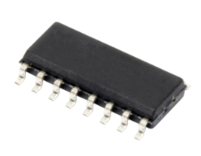
Analog Devices Inc.The ADuM141ES are quad-channel digital isolators based on Analog Devices, Inc., iCoupler? technology. Combining high speed, complementary metal-oxide semiconductor (CMOS) and monolithic air core transformer technology, these isolation components provide outstanding performance characteristics superior to alternatives such as optocoupler devices and other integrated couplers. The maximum propagation delay is 13.5 ns with a pulse width distortion of less than 3 ns at 5 V operation. Channel matching is tight at 3.0 ns maximum.The ADuM141ES data channels are independent and can with a withstand voltage rating of 400 V rms. This device operates with the supply voltage on either side ranging from 1.8 V to 5 V, providing compatibility with lower voltage systems as well as enabling voltage translation functionality across the isolation barrier.Unlike other optocoupler alternatives, dc correctness is ensured in the absence of input logic transitions. Two different fail-safe options are available, by which the outputs transition to a pre-determined state when the input power supply is not applied or the inputs are disabled.The ADuM141ES is packaged in a small 16-lead bottom brazed flatpack package for a 400 V rms isolation voltage rating.Applications Isolated data acquisition Isolated high speed data
EVAL-ADUM3151Z
Analog Devices Inc.The ADuM3151/ADuM3152/ADuM3153?are 7-channel, SPIsolator? digital isolators optimized for isolated serial peripheral interfaces (SPIs). Based on the Analog Devices, Inc., iCoupler? chip scale transformer technology, the low propagation delay in the CLK, MO/SI, MI/SO, and SS SPI bus signals supports SPI clock rates of up to 17 MHz. These channels operate with 14 ns propagation delay and 1 ns jitter to optimize timing for SPI.The ADuM3151/ADuM3152/ADuM3153 isolators also provide three additional independent low data rate isolation channels in three different channel direction combinations. Data in the slow channels is sampled and serialized for a 250 kbps data rate with up to 2.5 ?s of jitter in the low speed channels.Applications Industrial programmable logic controllers (PLCs) Sensor isolation?
EVAL-ADUM4122EBZ
Analog Devices Inc.The ADuM4122 is an isolated, single device, dual output driver that uses iCoupler? technology to provide precision isolation. The ADuM4122 provides 5 kV rms isolation in the wide-body, 8-lead SOIC package. These isolation components combine high speed complementary metal-oxide semiconductor (CMOS) and monolithic transformer technology to provide performance characteristics superior to alternatives (such as a combination of pulse transformers and gate drivers).The ADuM4122 operates with an input supply voltage range from 3.3 V to 6.5 V, providing compatibility with lower voltage systems. Unlike gate drivers that employ high voltage level translation methodologies, the ADuM4122 offers true galvanic isolation between the input and the output regions.The ADuM4122 includes two output pins that facilitate slew rate control of two output drive strengths. The VOUT pin follows the logic of the VIN+ pin, while the boosting output, VOUT_SRC, can be toggled to follow the VIN+ pin or to go high-Z. The toggling of the slew rate is controlled by the primary side. Slew rate control can allow for electromagnetic interference (EMI) mitigation and voltage overshoot control.An internal thermal shutdown sets outputs low if internal temperatures on the ADuM4122 exceed the thermal shutdown temperature.As a result, the ADuM4122 provides reliable control over the switching characteristics of insulated gate bipolar transistor (IGBT) and metal-oxide semiconductor field effect transistor (MOSFET) configurations over a wide range of switching voltages, allowing for simple slew rate control.Applications Switching power supplies Isolated IGBT and MOSFET gate drivers Industrial inverters
EVAL-ADUM4221EBZ
Analog Devices Inc.The ADuM4221/ADuM4221-1/ADuM4221-2 are 4 A isolated, half bridge gate drivers that employ the Analog Devices, Inc., iCoupler? technology to provide independent and isolated high-side and low-side outputs. The ADuM4221/ADuM4221-1/ADuM4221-2 provide 5700 V rms isolation in an increased creepage wide body, 16-lead SOIC_IC. Combining high speed CMOS and monolithic transformer technology, these isolation components provide outstanding performance characteristics superior to the alternatives, such as the combination of pulse transformers and gate drivers.The isolators operate with a logic input voltage ranging from 2.5 V to 6.5 V, providing compatibility with lower voltage systems. In comparison to gate drivers employing high voltage level translation methodologies, the ADuM4221/ADuM4221-1/ADuM4221-2 offer the benefit of true, galvanic isolation between the input and each output.The ADuM4221/ADuM4221-1/ADuM4221-2 each have built in overlap protection and allow dead time adjustment. A single resistor between the dead time pin (DT) and the GND1 pin sets the dead time on the secondary side between the high-side and the low-side outputs.An internal thermal shutdown (TSD) sets outputs low if the internal temperature on the ADuM4221/ADuM4221-1/ADuM4221-2 exceeds the TSD temperature. As a result, the ADuM4221/ADuM4221-1/ADuM4221-2 provide reliable control over the switching characteristics of the insulated gate bipolar transistor (IGBT)/metal-oxide semiconductor field effect transistor (MOSFET) configurations over a wide range of positive or negative switching voltages.Applications Switching power supplies Isolated IGBT/MOSFET gate drives Industrial inverters Gallium nitride (GaN)/silicon carbide (SiC) compatible1 Protected by U.S. Patents 5,952,849; 6,873,065; 7,075,239. Other patents pending.
EVAL-ADUM5010EBZ
Analog Devices Inc.The ADuM5010 is an integrated, isolated DC/DC converter.Based on the Analog Devices, Inc.,?iCoupler? technology, theDC/DC converter provides regulated, isolated power, adjustablebetween 3.15 V and 5.25 V. Input supply voltages can range fromslightly below the required output to significantly higher.The?iCoupler chip-scale transformer technology is used for isolated logic signals and for the magnetic components of the DC/DC converter. The result is a small form factor, total isolation solution.APPLICATIONS Power supply startup bias and gate drives Isolated sensor interfaces Industrial PLCs
EVAL-ADUM5411EBZ
Analog Devices Inc.The ADuM5410/ADuM5411/ADuM5412 are quad-channel digital isolators with isoPower?, integrated, isolated dc-to-dcconverters. Based on the Analog Devices, Inc., iCoupler? technology, the dc-to-dc converters provide regulated, isolated power that is adjustable between 3.15 V and 5.25 V.The ADuM5410/ADuM5411/ADuM5412 eliminate the need for a separate, isolated dc-to-dc converter in low power, isolated designs. The iCoupler chip scale transformer technology is used for isolated logic signals and for the magnetic components of the dc-to-dc converters. The result is a small form factor, total isolation solution.The ADuM5410/ADuM5411/ADuM5412 isolators provide fourindependent isolation channels in a variety of channel configurations and data rates (see the Ordering Guide for more information).Applications RS-232 transceivers Power supply startup bias and gate drives Isolated sensor interfaces Industrial PLCs
EVAL-ADV7180-32EBZ
Analog Devices Inc.The ADV7180 automatically detects and converts standard analog baseband television signals compatible with worldwide NTSC, PAL, and SECAM standards into 4:2:2 component video data compatible with the 8-bit ITU-R BT.656 interface standard.The simple digital output interface connects gluelessly to a wide range of MPEG encoders, codecs, mobile video processors, and Analog Devices, Inc., digital video encoders, such as the ADV7391. External HS, VS, and FIELD signals provide timing references for LCD controllers and other video ASICs, if required. Accurate 10-bit analog-to-digital conversion provides professional quality video performance for consumer applications with true 8-bit data resolution. Three analog video input channels accept standard composite, S-video, or component video signals, supporting a wide range of consumer video sources. AGC and clamp-restore circuitry allow an input video signal peak-to-peak range to 1.0 V. Alternatively, these can be bypassed for manual settings.The line-locked clock output allows the output data rate, timing signals, and output clock signals to be synchronous, asynchronous, or line locked even with ?5% line length variation. Output control signals allow glueless interface connections in many applications. The ADV7180 is programmed via a 2-wire, serial bidirectional port (I2C? compatible) and is fabricated in a 1.8 V CMOS process. Its monolithic CMOS construction ensures greater functionality with lower power dissipation. LFCSP package options makes the decoder ideal for space-constrained portable applications. A 64-lead LQFP package is pin compatible with the ADV7181C.The 48-Lead LQFP, 40-lead LFCSP, and 32-lead LFCSP use one pin to output VS or FIELD.APPLICATIONS Digital camcorders and PDAs Low cost SDTV PIP decoder for digital TVs Multichannel DVRs for video security AV receivers and video transcoding PCI-/USB-based video capture and TV tuner cards Personal media players and recorders Smartphone/multimedia handsets In-car/automotive infotainment units Rearview camera/vehicle safety systems
EVAL-ADV7182EBZ
Analog Devices Inc.The ADV7182 automatically detects and converts standard analog baseband video signals compatible with worldwide NTSC, PAL, and SECAM standards into a 4:2:2 component video data stream. This video data stream is compatible with the 8-bit ITU-R BT.656 interface standard.External HS, VS, and FIELD signals can provide timing references for LCD controllers and other video ASICs. The accurate 10-bit analog-to-digital conversion provides professional quality video performance for consumer applications with true 8-bit data resolution. The analog video inputs accept both single-ended, pseudo-differential, and fully differential composite video signals as well as S-Video and YPbPr video signals, supporting a wide range of consumer and automotive video sources.The ADV7182 along with an external resistor divider provide a common-mode input range of 4 V, enabling the removal of large signal, common-mode transients present on the video lines. Common-mode rejection (CMR) values of up to 80 dB can be achieved without the need for external amplifier circuitry.The AGC and clamp restore circuitry allow an input video signal peak-to-peak range to 1.0 V at the analog video input pin of the ADV7182. Alternatively, these can be bypassed for manual settings.The ADV7182 can be protected from short-to-battery (STB) events with standard ac coupling capacitors.The line-locked clock output allows the output data rate, timing signals, and output clock signals to be synchronous, asynchronous, or line locked even with ?5% line length variation. The ADV7182 is programmed via a two-wire, serial bidirectional port (I2C? compatible) and is fabricated in a 1.8 V CMOS process. Its monolithic CMOS construction ensures greater functionality with lower power dissipation. The LFCSP package options make the decoder ideal for space-constrained portable applications. The ADV7182 is a versatile one-chip multiformat video decoder that automatically detects PAL, NTSC, and SECAM standards in the form of composite, S-Video, and component video. The ADV7182 can receive composite signals in either single-ended or differential modes. This makes the ADV7182 ideal for automotive applications.The ADV7182 converts these analog video formats into a digital 8-bit ITU-R BT.656 video stream.The digital video output stream of the ADV7182 interfaces easily to a wide range of MPEG encoders, codecs, mobile video processors, and Analog Devices, Inc., digital video encoders, such as the ADV7391. External HS, VS, and FIELD signals provide timing references for LCD controllers and other video ASICs. APPLICATIONS Automotive infotainment DVRs for video security Media players
EVAL-ADV7281MAEBZ
Analog Devices Inc.The ADV7281 / ADV7281-M / ADV7281-MA are versatile one-chip, multiformat video decoders. The ADV7281/ ADV7281-M/ADV7281-MA automatically detect standard analog baseband video signals compatible with worldwide NTSC, PAL, and SECAM standards in the form of composite, S-Video, and component video.The ADV7281 converts the analog video signals into a YCrCb 4:2:2 video data stream that is compatible with the 8-bit ITU-R BT.656 interface standard.The ADV7281-M / ADV7281-MA convert the analog video signals into an 8-bit YCrCb 4:2:2 video data stream that is output over a mobile industry processor interface (MIPI?) CSI-2 interface.The analog video inputs of the ADV7281 / ADV7281-M / ADV7281-MA accept single-ended, pseudo differential, and fully differential signals. The ADV7281 provides four analog inputs and two STB diagnostic pins. The ADV7281-M provides six analog inputs, two STB diagnostic pins, and three general-purpose outputs. The ADV7281-MA provides eight analog inputs and three general-purpose outputs.The ADV7281 / ADV7281-M / ADV7281-MA are programmed via a 2-wire, serial bidirectional port (I2C compatible) and are fabricated in a 1.8 V CMOS process. The LFCSP package option makes these decoders ideal for space-constrained portable applications.APPLICATIONS Smartphone/multimedia handsets Automotive infotainment DVRs for video security Media players
ADV7281MEBZ Evaluation Board
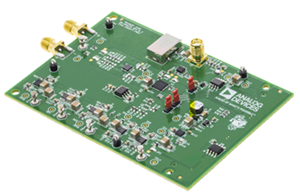
Analog Devices Inc.The EVAL-ADV7281MEBZ is an evaluation board for the ADV7281-M. Analog video is fed into the Video Inputs (Ain1 to Ain6). The EVAL-ADV7281MEBZ can receive analog video in a variety of different formats.
EVAL-ADV7281MEBZ converts analog video into an MIPI® CSI-2 output (8-bit YCrCb 4:2:2).
The MIPI® CSI-2 output of the consists of one differential data lane (D0+ and D0-) and one differential clock lane (Clk+ and Clk-). These are output to the SMA connectors on the EVAL-ADV7281MEBZ.
LTC2299IUP | DeMUX Dual ADC, +3.0V, 80Msps, 14Bit, 70MHz < AIN < 140MHz, (Requires DC890)
Analog Devices Inc.DC851A-F: Demo Board for the LTC2299 Dual 14-Bit, 80Msps Low Power 3V ADC.
LTC2292IUP | DeMUX Dual ADC, +3.0V, 40Msps 12-Bit 1MHz < AIN < 70MHz, (Requires DC890)
Analog Devices Inc.DC851A-J: Demo Board for the LTC2292 Dual 12-Bit, 40Msps Low Power 3V ADCs.
LTC2291IUP | DeMUX Dual ADC, +3.0V, 25Msps 12-Bit 1MHz < AIN < 70MHz, (Requires DC890)
Analog Devices Inc.DC851A-K: Demo Board for the LTC2291 Dual 12-Bit, 25Msps Low Power 3V ADCs.
LTC2288IUP | DeMUX Dual ADC, +3.0V, 65Msps 10-Bit 1MHz < AIN < 70MHz, (Requires DC890)
Analog Devices Inc.DC851A-P: Demo Board for the LTC2288 Dual 10-Bit, 65Msps Low Noise 3V ADCs.


