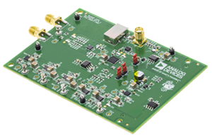
LTC3452EUF Demo Board
Analog Devices Inc.DC928A: Demo Board for the LTC3452 Synchronous Buck-Boost MAIN/CAMERA White LED Driver.
DC939A
Analog Devices Inc.The LTC2484 combines a 24-bit No Latency ??? analog-to-digital converter with patented Easy Drive? technology. The patented sampling scheme eliminates dynamic input current errors and the shortcomings of on-chip buffering through automatic cancellation of differential input current. This allows large external source impedances and input signals with rail-to-rail input range to be directly digitized while maintaining exceptional DC accuracy.The LTC2484 includes an on-chip oscillator. The LTC2484 can be configured to reject line frequencies. 50Hz, 60Hz or simultaneous 50Hz/60Hz line frequency rejection can be selected as well as a 2? speed-up mode.The LTC2484 allows a wide common mode input range (0V to VCC) independent of the reference voltage. The reference can be as low as 100mV or can be tied directly to VCC. The LTC2484 includes an on-chip trimmed oscillator, eliminating the need for external crystals or oscillators. Absolute accuracy and low drift are automatically maintained through continuous, transparent, offset and full-scale calibration.Applications Direct Sensor Digitizer Weight Scales Direct Temperature Measurement Strain Gauge Transducers Instrumentation Industrial Process Control DVMs and Meters
DC949A-B
Analog Devices Inc.The LT3478/LT3478-1 are 4.5A step-up DC/DC converters designed to drive LEDs with a constant current over a wide programmable range. Series connection of the LEDs provides identical LED currents for uniform brightness without the need for ballast resistors and expensive factory calibration.The LT3478-1 reduces external component count and cost by integrating the LED current sense resistor. The LT3478 uses an external sense resistor to extend the maximum programmable LED current beyond 1A and also to achieve greater accuracy when programming low LED currents. Operating frequency can be set with an external resistor from 200kHz up to 2.25MHz. Unique circuitry allows a PWM dimming range up to 3000:1 while maintaining constant LED color. The LT3478/LT3478-1 are ideal for high power LED driver applications such as automotive TFT LCD backlights, courtesy lighting and heads-up displays. One of two CTRL pins can be used to program maximum LED current. The other CTRL pin can be used to program a reduction in maximum LED current vs temperature to maximize LED usage and improve reliability.Additional features include inrush current protection, programmable open LED protection and programmable soft-start. Each part is available in a 16-pin thermally enhanced TSSOP Package.Applications High Power LED Driver Automotive Lighting
LTC3810EG Demo Board | 13V ≤ VIN ≤ 80V; VOUT = 12V @ 6A
Analog Devices Inc.Demonstration circuit 952 is a current mode synchronous switching regulator featuring the LTC3810. The circuit is configured as a synchronous step-down regulator operating at 230kHz switching frequency. Output voltage is 12V at 6A maximum load. The input voltage range is 13V to 80V.
LTC3824EMSE Demo Board | 5.5V ≤ VIN ≤ 60V, VOUT: 5V/2A
Analog Devices Inc.Demonstration circuit 960 is a high voltage, current-mode DC/DC step-down controller featuring the LTC3824 in a small 10-pin MSOP package.
The board operates from an input voltage of 5.5V to 60V and outputs 5V @ 2A. The converter uses a P-channel MOSFET for the main switch resulting in a low parts count design. Operating frequency is set to 200kHz with the option to accept a synchronized external clock.
LTC3835EGN-1 Demo Board | 4.5V ≤ VIN ≤ 36V, VOUT = 3.3V @ 5A
Analog Devices Inc.Demonstration circuit 965A is a single output high frequency step-down DC/DC converter featuring the low quiescent current LTC3835-1 in a 16-pin narrow SSOP package. The DC965A is programmed to generate a regulated 3.3V@5A output from a 4.5V to 36V input voltage. The LTC3835-1 is similar to the LTC3835 but has reduced functionality (it does not have PGOOD, ExtVCC or CLOCKOUT pins).
LT1952EGN-1, LTC3900CS8, LT4430ES6 Demo Board | VIN = 34V-75V VOUT = 3.3V @ 30A
Analog Devices Inc.DC968A-A Demo Board for:
LT1952 Single Switch Synchronous Forward Controller
LTC3900 Synchronous Rectifier Driver for Forward Converters
LT4430 Secondary-Side Optocoupler Driver
LT1952EGN-1, LTC3900CS8, LT4430ES6 Demo Board | VIN = 18V-36V, VOUT = 5V @ 20A
Analog Devices Inc.DC968A-B Demo Board for:
LT1952 Single Switch Synchronous Forward Controller
LTC3900 Synchronous Rectifier Driver for Forward Converters
LT4430 Secondary-Side Optocoupler Driver
LTC3822EDD Demo Board (DFN) | 2.75V ≤ VIN ≤ 4.5V, VOUT = 1.8V @ 8A
Analog Devices Inc.Demonstration circuit 972A is a high efficiency synchronous step-down DC/DC converter featuring the LTC3822EDD controller and dual N-Channel MOSFETs. The demo board is capable of providing 1.8V/8A from a 2.75V to 4.5V input.
LTC4069EDC Demo Board
Analog Devices Inc.DC973A: Demo Board for the LTC4069 Standalone 750mA Li-Ion Battery Charger in 2 × 2 DFN with NTC Thermistor Input.
LT3496EUFD Demo Circuit | Buck-Mode Triple LED Driver, 3V ≤ VIN ≤ 45V, VLED up to 45V (x3)
Analog Devices Inc.Demonstration circuit 986 is a Triple Step-Down LED Driver featuring the LT3496EUFD. The LT3496 is a triple output DC/DC converter designed to operate as current sources for driving high current LEDs. Each ofthe three regulators on the demo board is independently operated. The default current for each output channel is 500mA. The output current should not exceed the rated current of the LEDs used. The maximum voltage of an LED string the demo board can drive is limited by the duty cycle and the input voltage of the LT3496.
The maximum power input voltage (PVIN ) is 45V. As a result, each channel of the demo board can drive up to ~31V total LED voltage. The LT3496's input voltage range is 3V to 30V (with 40V transients), however to minimize power dissipation the demo board uses a 3V to 5.5V supply.
LTC6400-8 3GHz Fully Differential ADC Driver Demo Circuit
Analog Devices Inc.DC987B-A: Demo Board for the LTC6400-8 2.2GHz Low Noise, Low Distortion Differential ADC Driver for DC-300MHz.
LTC6401-26 3GHz Fully Differential ADC Driver Demo Circuit
Analog Devices Inc.DC987B-H: Demo Board for the LTC6401-26 1.6GHz Low Noise, Low Distortion Differential ADC Driver for DC-140MHz.
DC989B-A
Analog Devices Inc.The LTC3872 is a constant frequency current mode boost DC/DC controller that drives an N-channel power MOSFET and requires very few external components. The No RSENSE? architecture eliminates the need for a sense resistor, improves efficiency and saves board space.The LTC3872 provides excellent AC and DC load and line regulation with ?1.5% output voltage accuracy. It incorporates an undervoltage lockout feature that shuts down the device when the input voltage falls below 2.3V.High switching frequency of 550kHz allows the use of a small inductor. The LTC3872 is available in an 8-lead low profile (1mm) ThinSOT? package and 8-pin 2mm ? 3mm DFN package. LTC3872 LTC3872-1 Frequency Foldback In Current Limit Yes No Applications Telecom Power Supplies 42V Automotive Systems 24V Industrial Controls IP Phone Power Supplies
LT3080EDD Demo Board | Single Resistor Prog Linear Regulator, 2.3V ≤ VIN ≤ 25V, VOUT = 0.6V/1.0V/1.2V/1.5V/1.8V/2.5V/3.3V/5V @ 1.1A
Analog Devices Inc.Demonstration circuit 995A is an adjustable 1.1A linear regulator featuring the LT3080. Architected as a precision current source and voltage follower, it allows this new regulator to be used in many applications requiring high current, adjustability to zero output, and no heat sink. The device brings out the collector of the pass transistor to allow low dropout operation when used with multiple supplies. The demo board's input supply voltage range is 2.3V to 25V. For proper regulation, the LT3080 has a control pin; the voltage on this pin must be 1.2V to 1.35V higher than the output voltage.The output voltage is jumper selectable and can be set to 1.8V, a value between 0V and 5V (using trimpot R2) or a user-defined value.
A key feature of the LT3080 is its wide output voltage range. By using a reference current through a single resistor, the output voltage can be programmed to any level between zero and 36V. The DC995A has a reduced input voltage 25V due to input capacitor voltage rating. The DC995A can be used as a high current linear regulator, a post regulator for switching supply,a variable voltage supply or a low output voltage power supply.
LTC2242CUP-10 | LVDS OUT, VCC = 2.5V, 250Msps, 10-Bit, 10MHz < AIN < 250MHz, (Requires DC890 & LVDS_XFMR)
Analog Devices Inc.DC997B-D - Demo Board for the LTC2242-10 10-Bit, 250Msps ADC.
LTC3533EDE Demo Board | High Efficiency Synchronous Buck-Boost Converter
Analog Devices Inc.Demonstration circuit 999A is a wide input range, 3.3V, synchronous buck-boost converter featuring the LTC3533. This circuit is designed to demonstrate the high level of performance, efficiency and small solution size attainable using this part in a buck-boost power supply. It operates at 1MHz and produces a regulated 3.3V from an input voltage range of 2.4V to 5.5V, and operates down to 1.8V with de-rated output current.
EK1HMC1190ALP6N
Analog Devices Inc.The HMC1190ALP6NE is a high linearity broadband dual channel downconverting mixer with integrated PLL and VCO optimized for multi-standard receiver applications that require a compact, low power design. Integrated wideband limiting LO amplifiers enable the HMC1190ALP6NE to achieve an unprecedented RF bandwidth of 700 MHz to 3800 MHz for applications including Cellular/3G, LTE/WiMAX/4G. Unlike conventional narrow-band downconverters, the HMC1190ALP6NE supports both high-side and low-side LO injection over all RF frequencies. The RF and LO input ports are internally matched to 50 Ohms.The HMC1190ALP6NE features an integrated LO and RF baluns, enable control of IF and LO amplifiers and bias control interface to high linearity passive mixer cores. Balanced passive mixer combined with high-linearity IF amplifier architecture provides excellent LO-to-RF, LO-to-IF, and RF-to-IF isolations. Low noise figure of 9 dB, and high IIP3 of +24 dBm allow the HMC1190ALP6NE to be used in most demanding applications. External bias control pins enable optimization of already low power dissipation of 2.34 W (typical). Fast enable control interface reduces power consumption further in TDD applications.External VCO input allows the HMC1190ALP6NE to lock external VCOs, and enables cascaded LO architectures for MIMO applications. Two separate Charge Pump (CP) outputs enable separate loop filters optimized for both integrated and external VCOs, and seamless switching between integrated or external VCOs during operation. Programmable RF output phase features can further phase adjust and synchronize multiple HMC1190ALP6NEs enabling scalable MIMO and beam-forming radio architectures.Additional features include configurable LO output mute function, Exact Frequency Mode that enables the HMC1190ALP6NE to generate fractional frequencies with 0 Hz frequency error, and the ability to synchronously change frequencies without changing phase of the output signal that increases efficiency of digital pre-distortion loops. The HMC1190ALP6NE is housed in RoHS compliant compact 6x6 mm leadless QFN package.Applications Multiband/Multi-standard Cellular BTS?Diversity Receivers GSM & 3G & LTE/WiMAX/4G MIMO Infrastructure Receivers Wideband Radio Receivers Multiband Basestations & Repeaters
EK1HMC7043LP7F
Analog Devices Inc.The HMC7043 is designed to meet the requirements of multicarrier GSM and LTE base station designs, and offers a wide range of clock management and distribution features to simplify baseband and radio card clock tree designs.The HMC7043 provides 14 low noise and configurable outputs to offer flexibility in interfacing with many different components in a base transceiver station (BTS) system, such as data converters, local oscillators, transmit/receive modules, field programmable gate arrays (FPGAs), and digital front-end ASICs. The HMC7043 can generate up to seven DCLK and SYSREF clock pairs per the JESD204B/JESD204C interface requirements.The system designer can generate a lower number of DCLK and SYSREF pairs, and configure the remaining output signal paths for independent phase and frequency. Both the DCLK and SYSREF clock outputs can be configured to support different signaling standards, including CML, LVDS, LVPECL, and LVCMOS, and different bias conditions to adjust for varying board insertion losses. One of the unique features of the HMC7043 is the independent flexible phase management of each of the 14 channels. All 14 channels feature both frequency and phase adjustment. The outputs can also be programmed for 50 ? or 100 ? internal and external termination options. The HMC7043 device features an RF SYNC feature that synchronizes multiple HMC7043 devices deterministically, that is, ensures that all clock outputs start with the same edge. This operation is achieved by rephrasing the nested HMC7043 or SYSREF control unit/divider, deterministically, and then restarting the output dividers with this new phase. The HMC7043 is offered in a 48-lead, 7 mm ? 7 mm LFCSP package with an exposed pad connected to ground. Applications JESD204B/JESD204C clock generation Cellular infrastructure (multicarrier GSM, LTE, W-CDMA) Data converter clocking Phase array reference distribution Microwave baseband cards
EKIT01-HMC1033LP6G
Analog Devices Inc.The HMC1033LP6GE is a low-noise, wide-band 3.3 V clock generator IC with a fractional-N Phase Locked Loop (PLL) that features an integrated Voltage Controlled Oscillator (VCO). The device provides differential clock outputs between 25 MHz and 550 MHz range. The HMC1033LP6GE features a low noise Phase Detector (PD) and Delta- Sigma modulator, capable of operating at up to 100 MHz which permits wider loop-bandwidths and excellent spurious performance.The HMC1033LP6GE features industry leading phase noise and jitter performance, across the operating range, that enable it to improve link level jitter performance, Bit-Error-Rates (BER) and eye diagram metrics. The superior noise floor (


