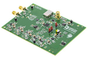
AD9956-VCO/PCBZ
Analog Devices Inc.The AD9956 is Analog Devices?s first AgileRF synthesizer.The device is comprised of a DDS and PLL circuitry. The DDSfeatures a 14-bit DAC operating up to 400 MSPS and a 48-bitfrequency tuning word. The PLL Circuitry includes a phasedetector with scaleable 200 MHz inputs (pre-scalar inputsoperate up to 650 MHz) and digital control over the chargepump current. The device also includes a 650 MHz PECL driverwith programmable slew rates.The AD9956 uses advanced DDStechnology, an internal high-speed, high performance D/Aconverter and an advance phase-detector/charge pumpcombination to enable the synthesis of digitally-programmable,frequency-agile analog output sinusoidal waveforms up to2.7 GHz. The AD9956 is designed to provide fast frequencyhopping and fine tuning resolution (48-bit frequency tuningword). Information is loaded into the AD9956 via a serial I/Oport which has a device write speed of 25 MBit/sec. The AD9956DDS block also supports a user defined linear sweep mode ofoperation.The AD9956 is specified to operate over the extendedautomotive range of ?40?C to +125?C.Applications Agile LO frequency synthesis FM chirp source for radar and scanning systems Automotive radars Test and measurement equipment Acousto-optic device drivers
AD9957/PCBZ
Analog Devices Inc.The AD9957 functions as a universal I/Q modulator and agileupconverter for communications systems where cost, size, powerconsumption, and dynamic performance are critical. TheAD9957 integrates a high speed, direct digital synthesizer(DDS), a high performance, high speed, 14-bit digital-to-analogconverter (DAC), clock multiplier circuitry, digital filters, andother DSP functions onto a single chip. It provides basebandupconversion for data transmission in a wired or wirelesscommunications system.The AD9957 is the third offering in a family of quadraturedigital upconverters (QDUCs) that includes the AD9857 andAD9856. It offers performance gains in operating speed, powerconsumption, and spectral performance. Unlike its predecessors,it supports a 16-bit serial input mode for I/Q baseband data.The device can alternatively be programmed to operate either asa single tone, sinusoidal source or as an interpolating DAC.The reference clock input circuitry includes a crystal oscillator,a high speed, divide-by-two input, and a low noise PLL formultiplication of the reference clock frequency.The user interface to the control functions includes a serial porteasily configured to interface to the SPORT of the Blackfin?DSP and profile pins to enable fast and easy shift keying of anysignal parameter (phase, frequency, or amplitude).Applications HFC data, telephony, and video modems Wireless base station transmissions Broadband communications transmissions Internet telephony
AD9961-EBZ
Analog Devices Inc.The AD9961/AD9963 are pin-compatible, 10-/12-bit, lowpower MxFE? converters that provide two ADC channels withsample rates of 100 MSPS and two DAC channels with samplerates to 170 MSPS. These converters are optimized for transmit and receive signal paths of communication systems requiring lowpower and low cost. The digital interfaces provide flexibleclocking options. The transmit is configurable for 1?, 2?, 4?, and 8? interpolation. The receive path has a bypassable 2? decimating low-pass filter.The AD9961 and AD9963 have five auxiliary analog channels.Three are inputs to a 12-bit ADC. Two of these inputs can beconfigured as outputs by enabling 10-bit DACs. The other two channels are dedicated outputs from two independent 12-bit DACs.The high level of integrated functionality, small size, and lowpower dissipation of the AD9961/AD9963 make them well-suited for portable and low power applications.APPLICATIONS Wireless infrastructure Picocell, femtocell basestations Medical instrumentation Ultrasound AFE Portable instrumentation Signal generators, signal analyzers
ADA2200-EVALZ
Analog Devices Inc.The ADA2200 is a synchronous demodulator and configurable analog filter designed to perform precision magnitude and phase measurements in low power, sensor signal conditioning and data acquisition applications for the industrial, medical, and communications markets. Implemented with ADI?s patent pending sampled analog technology (SAT), the ADA2200 is an analog input, sampled analog output device that includes an analog domain, low-pass 1/8x decimation finite impulse response (FIR) filter, a configurable infinite impulse response (IIR) filter, mixer with 0?/90? phase selection, reference clock and ADC driver output. Utilizing sampled analog technology, the signal processing is performed entirely in the analog domain by charge sharing among capacitors, which eliminates the effects of quantization noise and rounding errors and reduces downstream ADC sample rates while also offloading computationally heavy tasks from the digital processor or micro-controller.The ADA2200 acts as a precision filter when the demodulation function is disabled. The filter has a programmable bandwidth and tunable center frequency. The filter characteristics are highly stable over temperature, supply, and process variation.Single-ended and differential signal interfaces are possible on both input and output terminals, simplifying the connection to other components of the signal chain. The low power consumption and rail-to-rail operation is ideal for battery-powered and low voltage systems.The ADA2200 can be programmed over its SPI-compatible serial port or can automatically boot from the EEPROM through its I2C interface. On-chip clock generation produces a mixing signal with a programmable frequency and phase. In addition, the ADA2200 synchronization output signal eases interfacing to other sampled systems, such as data converters and multiplexers.The ADA2200 is available in a 16-lead TSSOP package. Its performance is specified over the industrial temperature range of ?40?C to +85?C. Note that throughout this data sheet, multifunction pins, such as SCLK/SCL, are referred to either by the entire pin name or by a single function of the pin, for example, SCLK, when only that function is relevant.Applications Synchronous demodulation Sensor signal conditioning Lock-in amplifiers Phase detectors Precision tunable Filters Signal recovery Control systems
ADA4254CP-EBZ
Analog Devices Inc.The ADA4254 is a zero drift, high voltage, low power?programmable gain instrumentation amplifier (PGIA) designed?for process control and industrial applications. The ADA4254?features 12 binary weighted gains ranging from 1/16 V/V to?128 V/V and three scaling gain options of 1 V/V, 1.25 V/V, and?1.375 V/V, resulting in 36 possible gain settings. The power?consumption of the ADA4254 is a mere 22 mW, making the?device an excellent choice for industrial systems that demand?precision, robustness, and low power.The zero drift amplifier topology of the ADA4254 self calibrates dc errors and low frequency 1/f noise, achieving excellent dc precision over the entire specified temperature range. This high level of precision maximizes dynamic range and greatly reduces calibration requirements in many applications.?The input multiplexer provides ?60 V protection to the high impedance inputs of the amplifier, while providing the capability to switch between two input sources. In addition, integrated electromagnetic interference (EMI) filters block harsh RF noise from the sensitive inputs of the amplifier.?Various safety features on the ADA4254 detect both internal and external faults. The serial port interface (SPI) supports cyclical redundancy check (CRC) error detection to ensure robust communication. These safety features ease system safety integrity level (SIL) certification.?Seven general-purpose input/output (GPIO) pins, which can be configured to provide various special functions, are included in the ADA4254. An excitation current source output is available to bias sensors such as resistance temperature detectors (RTDs).?The ADA4254 is specified over the ?40?C to +105?C temperature range and is offered in a compact 5 mm ? 5 mm, 28-lead LFCSP and a 24-lead TSSOP.?Applications Universal process control front ends Data acquisition systems Test and measurement systems?
ADA4255CP-EBZ
Analog Devices Inc.The ADA4255 is a precision programmable gain instrumentation amplifier (PGIA) with integrated bipolar charge pumps. With its integrated charge pumps, the ADA4255 internally produces the high voltage bipolar supplies needed to achieve a wide input voltage range (38 V typical with VDDCP = 5 V) without lowering input impedance. The charge pump topology of the ADA4255 allows channels to be isolated with only low voltage components, reducing complexity, size, and implementation time in industrial and process control systems.The zero drift PGIA topology of the ADA4255 self calibrates dc errors and lower frequency 1/f noise, achieving excellent dc precision over the entire specified temperature range. The combination of 36 precision gains ranging from 1/16 V/V to 176 V/V within the ADA4255 and high voltage, high impedance inputs allow a wide range of inputs to be scaled to the range of the analog-to-digital converter (ADC). By integrating all gain setting and level shifting resistors, the ADA4255 achieves excellent common-mode rejection ratio (CMRR) performance (111 dB minimum at G = 1 V/V) and extremely low gain drift (?1 ppm/?C maximum). This high level of precision maximizes dynamic range and greatly reduces calibration requirements in many applications.The ?60 V input protection, integrated electromagnetic interference (EMI) filtering and various safety features make the ADA4255 an ideal choice for robust industrial systems. Seven general-purpose input and output (GPIOx) pins, which can be configured to provide various special functions, are included in the ADA4255. An excitation current source output is available to bias sensors such as resistance temperature detectors (RTDs).The ADA4255 is specified over the ?40?C to +105?C temperature range and is offered in a compact 5 mm ? 5 mm, 28-lead LFCSP.APPLICATIONSUniversal process control front endsData acquisition systemsTest and measurement systemsSystem power monitoring
ADA4433-1BCP-EBZ
Analog Devices Inc.The ?ADA4433-1 is a differential output, fully integrated video reconstruction filter that combines overvoltage protection (short-to-battery [STB] protection) and short-to-ground (STG) protection on the outputs, with excellent video specifications and low power consumption. The combination of STB protection and robust ESD tolerance allows the ADA4433-1 to provide superior protection in the hostile automotive environment.The ADA4433-1 is a fully differential video filter that can be used as a fully differential input to a differential output or as a single-ended input to a differential output, allowing it to easily connect to both differential and single-ended sources. It is capable of driving twisted pair or coaxial cable with minimal line attenuation. Differential signal processing reduces the effects of ground noise, which can plague ground referenced systems. The ADA4433-1 is ideal for differential signal processing (gain and filtering) throughout the signal chain, simplifying the conversion between single-ended and differential components.The short-to-battery protection integrated into the ADA4433-1 protects against both dc and transient overvoltage events, caused by an accidental short to a battery voltage up to 18 V. The Analog Devices, Inc., short-to-battery protection eliminates the need for large output coupling capacitors and other complicated circuits used to protect standard video amplifiers, saving space and cost.The ADA4433-1 features a high-order filter with ?3 dB cutoff frequency response at 10 MHz and 45 dB of rejection at 27 MHz. The ADA4433-1 featurea an internally fixed gain of 2 V/V. This makes the ADA4433-1 ideal for SD video applications, including NTSC and PAL.The ADA4433-1 operates on single supplies as low as 2.6 V and as high as 3.6 V while providing the dynamic range required by the most demanding video systems.The ADA4433-1 is offered in an 8-lead, 3 mm ? 3 mm LFCSP package, rated for operation over the wide automotive temperature range of ?40?C to +125?C.Appplications Automotive rearview cameras Automotive video electronic control units (ECUs) Surveillance video systems
ADA4857-2YCP-EBZ
Analog Devices Inc.The ADA4857 is a unity gain stable, high speed, voltage feedback amplifier with low distortion, low noise, and high slew rate. With a spurious-free dynamic range (SFDR) of ?88 dBc @ 10 MHz, the ADA4857 is an ideal solution for a variety of applications including ultrasounds, ATE, active filters, and ADC drivers. The Analog Devices, Inc., proprietary next-generation XFCB process and innovative architecture enables such high performance amplifiers. The ADA4857 has 850 MHz bandwidth, 2800 V/?s slew rate, and settles to 0.1% in 15 ns. With a wide supply voltage range (5 V to 10 V), the ADA4857 is an ideal candidate for systems that require high dynamic range, precision, and speed. The ADA4857-1 amplifier is available in a 3 mm ? 3 mm, 8-lead LFCSP and a standard 8-lead SOIC. The ADA4857-2 is available in a 4 mm ? 4 mm, 16-lead LFSCP. The LFCSP features an exposed paddle that provides a low thermal resistance path to the printed circuit board (PCB). This path enables more efficient heat transfer and increases reliability. The ADA4857 works over the extended industrial temperature range (?40?C to +125?C). ApplicationsInstrumentationIF and baseband amplifiersActive filtersADC driversDAC bufferstable.nopad td, table.nopad th { padding: 0px; margin: 0px; vertical-align: top;}
ADA4870ARR-EBZ
Analog Devices Inc.The ADA4870 is a unity gain stable, high speed current feedback amplifier capable of delivering 1 A of output current and 2500 V/?s slew rate from a 40 V supply. Manufactured using the Analog Devices, Inc., proprietary high voltage extra fast complementary bipolar (XFCB) process, the innovative architecture of the ADA4870 enables high output power, high speed signal processing solutions in applications that require driving a low impedance load.The ADA4870 is ideal for driving high voltage power FETs, piezo transducers, PIN diodes, CCD panels, and a variety of other demanding applications that require high speed from high supply voltage at high output current.The ADA4870 is available in a power SOIC package (PSOP_3), featuring an exposed thermal slug that provides high thermal conductivity, enabling efficient heat transfer for improved perfor-mance and reliability in demanding applications. The ADA4870 operates over the industrial temperature range (?40?C to +85?C).Applications Envelope tracking Power FET driver Ultrasound Piezo drivers PIN diode drivers Waveform generation Automated test equipment (ATE) CCD panel drivers Composite amplifiers
ADA4891-3AR-EBZ
Analog Devices Inc.The ADA4891-1 (single), ADA4891-2 (dual), ADA4891-3 (triple), and ADA4891-4 (quad) are CMOS, high speed amplifiers that offer high performance at a low cost. The amplifiers feature true single-supply capability, with an input voltage range that extends 300 mV below the negative rail.In spite of their low cost, the ADA4891 family provides high performance and versatility. The rail-to-rail output stage enables the output to swing within 50 mV of each rail, enabling maximum dynamic range.The ADA4891 family of amplifiers is ideal for imaging applications, such as consumer video, CCD buffers, and contact image sensor buffers. Low distortion and fast settling time also make them ideal for active filter applications.The ADA4891-1/ADA4891-2/ADA4891-3/ADA4891-4 are available in a wide variety of packages.The ADA4891-1 is available in 8-lead SOIC and 5-lead SOT-23 packages.The ADA4891-2 is available in 8-lead SOIC and 8-lead MSOP packages.The ADA4891-3 and ADA4891-4 are available in 14-lead SOIC and 14-lead TSSOP packages.The amplifiers are specified to operate over the extended temperature range of ?40?C to +125?C.Applications Imaging Consumer video Active filters Coaxial cable drivers Clock buffers Photodiode preamp Contact image sensor and buffers
ADA4891-3ARU-EBZ
Analog Devices Inc.The ADA4891-1 (single), ADA4891-2 (dual), ADA4891-3 (triple), and ADA4891-4 (quad) are CMOS, high speed amplifiers that offer high performance at a low cost. The amplifiers feature true single-supply capability, with an input voltage range that extends 300 mV below the negative rail.In spite of their low cost, the ADA4891 family provides high performance and versatility. The rail-to-rail output stage enables the output to swing within 50 mV of each rail, enabling maximum dynamic range.The ADA4891 family of amplifiers is ideal for imaging applications, such as consumer video, CCD buffers, and contact image sensor buffers. Low distortion and fast settling time also make them ideal for active filter applications.The ADA4891-1/ADA4891-2/ADA4891-3/ADA4891-4 are available in a wide variety of packages.The ADA4891-1 is available in 8-lead SOIC and 5-lead SOT-23 packages.The ADA4891-2 is available in 8-lead SOIC and 8-lead MSOP packages.The ADA4891-3 and ADA4891-4 are available in 14-lead SOIC and 14-lead TSSOP packages.The amplifiers are specified to operate over the extended temperature range of ?40?C to +125?C.Applications Imaging Consumer video Active filters Coaxial cable drivers Clock buffers Photodiode preamp Contact image sensor and buffers
ADA4960-1ACP-EBZ
Analog Devices Inc.The ADA4960-1 is a high performance, differential amplifier optimized for RF and IF applications. It achieves better than 63 dB IMD3 performance for frequencies up to and beyond 1 GHz, making it an ideal driver for 8-bit to 10-bit giga-sample analog-to-digital converters (ADCs).The buffered inputs of the ADA4960-1 isolate the gain-setting resistor (RG) from the signal inputs, maintaining a constant 10 k? input resistance, easing matching and input drive requirements. The ADA4960-1 has a nominal 150 ? differential output impedance.The ADA4960-1 is optimized for wideband, low distortion performance for frequencies up to and beyond 1 GHz. These attributes, together with its adjustable gain capability, make this device the amplifier of choice for general-purpose IF and broadband applications where low distortion, noise, and power are critical.The device is optimized for the best combination of slew rate, bandwidth, and broadband distortion. These attributes allow it to drive a wide variety of ADCs. It is ideally suited for driving mixers, pin diode attenuators, SAW filters, and multi-element discrete devices.The user accessible gain adjust and bandwidth extension features allow configuration of the ADA4960-1 for line driver and channel equalization applications.The quiescent current of the ADA4960-1 is typically 60 mA. When disabled, it consumes less than 3 mA, offering excellent input-to-output isolation.Fabricated on an Analog Devices, Inc., high speed SiGe process, the ADA4960-1 is available in a compact 3 mm ? 3 mm, 16-lead LFCSP. It operates over the temperature range of ?40?C to +85?C.Applications Differential ADC drivers for giga-sample ADCs GBPS line drivers with pre-emphasis High speed data acquisition Electronic surveillance countermeasures Pulse capture and conditioning Oscilloscopes Satellite communications Single-ended-to-differential converters RF/IF gain blocks
ADAR1000EVAL1Z
Analog Devices Inc.The ADAR1000 is a 4-channel, X and Ku frequency band, beamforming core chip for phased arrays. This device operates in half-duplex between receive and transmit modes. In receive mode, input signals pass through four receive channels and are combined and output at the common RF_IO pin. In transmit mode, the RF_IO input signal is split and passes through the four transmit channels. In both modes, the ADAR1000 provides a ?31 dB gain adjustment range and a full 360? phase adjustment range in each radio frequency (RF) channel, with 6-bit resolution (less than ?0.5 dB and 2.8?, respectively).A simple 4-wire serial port interface (SPI) controls all of the on-chip registers. In addition, two address pins allow SPI control of up to four devices on the same serial lines. Dedicated transmit and receive load pins also provide synchronization of all ADAR1000 chips in the same array, and a single pin controls fast switching between the transmit and receive modes. The ADAR1000 is fabricated in a silicon-germanium, bipolar CMOS (BiCMOS) process. The device is available in a compact, 88-terminal, 7 mm ? 7 mm, LGA package and is specified from ?40?C to +85?C.APPLICATIONS Phased array radar Satellite communications systems
ADAR2001-EVALZ
Analog Devices Inc.The ADAR2001 is a transmitter IC optimized for millimeter wave body scanning applications. Accepting a single-ended continuous wave (CW) input signal between 2.5 GHz and 10 GHz, the ADAR2001 provides gain, 4? frequency multiplication, harmonic filtering, 1:4 signal splitting, and four independently controllable power amplifiers (PAs) with differential outputs designed to directly drive dipole antennas with differential inputs.All device functions and configuration options can be accessed by a 3-wire or 4-wire Analog Devices, Inc., serial peripheral interface (SPI).Two state machines are also integrated into the ADAR2001, which facilitate easy configuration, control, and fast switching of the frequency multiplier, filter, and transmitter sections. These sequencers are programmed through the SPI and are then operated by pulsed inputs (reset and advance).The output power and chip temperature can be monitored by four on-chip detectors and a temperature sensor whose outputs are multiplexed to an 8-bit ADC. The ADAR2001 requires only a single 2.5 V supply with power consumption of 450 mW with one channel turned on.The ADAR2001 is available in a compact, 40-terminal, 6 mm ? 6 mm LGA package and is specified from ?40?C to +85?C.APPLICATIONS Millimeter Wave Imaging Security Medical Industrial Wideband local oscillator (LO) multiplier/distributor
ADAR2004-EVALZ
Analog Devices Inc.The ADAR2004 is a 4-channel receiver IC that is optimized for millimeter wave body scanning applications. Accepting differential input signals from 10 GHz to 40 GHz, the ADAR2004 provides a low intermediate frequency (IF) output up to 800 MHz. Each receive channel also has independent gain control.The mixer local oscillator (LO) path includes a 4? multiplier requiring an applied LO frequency between 2.4 GHz and 10.1 GHz. The 4? multiplier block includes a programmable filter that helps keep harmonics down before reaching the mixer.Two programmable state machines are included to facilitate simple configuration, control, and fast switching of the frequency multiplier, filter, and receiver sections. These sequencers are programmed through the serial peripheral interface (SPI) and are then operated by pulsed inputs (reset and advance).The ADAR2004 requires only a single 2.5 V supply with power consumption of 910 mW with all channels turned on.The ADAR2004 is available in a 7 ? 7 mm, 48-terminal LGA package and is specified from ?40?C to +85?C.APPLICATIONS Millimeter wave imaging Security Medical Industrial Multichannel receivers
ADCLK846/PCBZ
Analog Devices Inc.The ADCLK846 is a 1.2 GHz/250 MHz, LVDS/CMOS, fanout buffer optimized for low jitter and low power operation. Possible configurations range from 6 LVDS to 12 CMOS outputs, including combinations of LVDS and CMOS outputs. Two control lines are used to determine whether fixed blocks of outputs are LVDS or CMOS outputs.The clock input accepts various types of single-ended and differential logic levels including LVPECL, LVDS, HSTL, CML, and CMOS.Table 8 provides interface options for each type of connection. The SLEEP pin enables a sleep mode to power down the device.This device is available in a 24-pin LFCSP package. It is specified for operation over the standard industrial temperature range of ?40?C to +85?C.APPLICATIONS Low jitter clock distribution Clock and data signal restoration Level translation Wireless communications Wired communications Medical and industrial imaging ATE and high performance instrumentation
ADCLK925/PCBZ
Analog Devices Inc.The ADCLK905 (one input, one output), ADCLK907 (dual oneinput, one output), and ADCLK925 (one input, two outputs) areultrafast clock/data buffers fabricated on the Analog Devices, Inc.,proprietary XFCB3 silicon germanium (SiGe) bipolar process.The ADCLK905/ADCLK907/ADCLK925 feature full-swing emitter coupled logic (ECL) output drivers. For PECL (positive ECL) operation, bias VCC to the positive supply and VEE to ground. For NECL (negative ECL) operation, bias VCC to ground and VEE to the negative supply.The buffers offer 95 ps propagation delay, 7.5 GHz toggle rate, 10 Gbps data rate, and 60 fs random jitter (RJ).The inputs have center tapped, 100 ?, on-chip termination resistors. A VREF pin is available for biasing ac-coupled inputs.The ECL output stages are designed to directly drive 800 mV each side into 50 ? terminated to VCC ? 2 V for a total differential output swing of 1.6 V.The ADCLK905/ADCLK907/ADCLK925 are available in 16-lead LFCSP packages.Applications Clock and data signal restoration and level shifting Automated test equipment (ATE) High speed instrumentation High speed line receivers Threshold detection Converter clocking
ADCLK944/PCBZ
Analog Devices Inc.The ADCLK944 is an ultrafast clock fanout buffer fabricated on the Analog Devices, Inc., proprietary XFCB3 silicon germanium (SiGe) bipolar process. This device is designed for high speed applications requiring low jitter.The device has a differential input equipped with center-tapped, differential, 100 ? on-chip termination resistors. The input can accept dc-coupled LVPECL, CML, 3.3 V CMOS (single-ended), and ac-coupled 1.8 V CMOS, LVDS, and LVPECL inputs. A VREF pin is available for biasing ac-coupled inputs.The ADCLK944 features four full-swing emitter-coupled logic (ECL) output drivers. For LVPECL (positive ECL) operation, bias VCC to the positive supply and VEE to ground. For ECL operation, bias VCC to ground and VEE to the negative supply.The ECL output stages are designed to directly drive 800 mV each side into 50 ? terminated to VCC ? 2 V for a total differential output swing of 1.6 V.The ADCLK944 is available in a 16-lead LFCSP and is specified for operation over the standard industrial temperature range of ?40?C to +85?C.?APPLICATIONS Low jitter clock distribution Clock and data signal restoration Level translation Wireless communications Wired communications Medical and industrial imaging ATE and high performance instrumentation
ADIS16203/PCBZ
Analog Devices Inc.The ADIS16203 is a complete incline-angle measurement system ina single compact package enabled by the Analog Devices, Inc.,iSensor? integration. By enhancing the Analog Devices iMEMS?sensor technology with an embedded signal processing solution, the ADIS16203 provides factory-calibrated, sensor-to-digital incline-angle data in a convenient format that can be accessed using aserial peripheral interface (SPI). The SPI interface provides access to multiple measurements: 360? linear inclination angles, ?180?linear incline angles, temperature, power supply, and one auxiliaryanalog input. Easy access to calibrated digital sensor data providesdevelopers with a system-ready device, reducing developmenttime, cost, and program risk.Unique characteristics of the end system are accommodatedeasily through several built-in features, such as a single-command offset calibration, along with convenient sample rate and band-width control.The ADIS16203 offers the following embedded features that eliminate the need for external circuitry and provide a simplified system interface: Configurable alarm function Auxiliary 12-bit analog-to-digital converter (ADC) Auxiliary 12-bit digital-to-analog converter (DAC) Configurable digital I/O port Digital self-test functionThe ADIS16203 offers two power management features formanaging system-level power dissipation: low power mode anda configurable shutdown feature.The ADIS16203 is available in a 9.2 mm ? 9.2 mm ? 3.9 mmlaminate-based land grid array (LGA) package with a temperature range of ?40?C to +125?C.APPLICATIONS Tilt sensing, inclinometers Platform control, stabilization, and leveling Motion/position measurement Monitor/alarm devices (security, medical, safety) Robotics
ADIS16209/PCBZ
Analog Devices Inc.The ADIS16209 is a high accuracy, digital inclinometer that accommodates both single-axis (?180?) and dual-axis (?90?) operation. The standard supply voltage (3.3 V) and serial peripheral interface (SPI) enable simple integration into most industrial system designs. A simple internal register structure handles all output data and configuration features. This includes access to the following output data: calibrated acceleration, accurate incline angles, power supply, internal temperature, auxiliary analog and digital input signals, diagnostic error flags, and programmable alarm conditions.Configurable operating parameters include sample rate, power management, digital filtering, auxiliary analog and digital output, offset/null adjustment, and self-test for sensor mechanical structure.The ADIS16209 is available in a 9.2 mm ? 9.2 mm ? 3.9 mm LGA package that operates over a temperature range of ?40?C to +125?C. It can be attached using standard RoHS-compliant solder reflow processes.APPLICATIONS Platform control, stabilization, and alignment Tilt sensing, inclinometers, leveling Motion/position measurement Monitor/alarm devices (security, medical, safety) Navigation


