DC1219A-C
Analog Devices Inc.The LT3495/LT3495B/LT3495-1/LT3495B-1 are low noise boost converters with integrated power switch, feedback resistor and output disconnect circuitry. The parts control power delivery by varying both the peak inductor current and switch off-time. This novel* control scheme results in low output voltage ripple as well as high efficiency over a wide load range. For the LT3495/LT3495-1, the off-time of the switch is not allowed to exceed a ?xed level, guaranteeing the switching frequency stays above the audio band for the entire load range. The parts feature a high performance NPN power switch with a 650mA and 350mA current limit for the LT3495/LT3495B and LT3495-1/LT3495B-1 respectively. The quiescent current is a low 60?A, which is further reduced to 0.1?A in shutdown. The internal disconnect circuitry allows the output voltage to be isolated from the input during shutdown. An auxiliary reference input (CTRL pin) overrides the internal 1.235V feedback reference with any lower value allowing full control of the output voltage during operation. The LT3495 series are available in a tiny 10-lead 3mm ? 2mm DFN package.Applications OLED Power Low Noise Power MP3 Player
DC1220B
Analog Devices Inc.The LTC3225/LTC3225-1 are programmable supercapacitor chargers designed to charge two supercapacitors in series to a selectable fixed output voltage (4.8V/5.3V for the LTC3225 and 4V/4.5V for the LTC3225-1) from input supplies as low as 2.8V to 5.5V. Automatic cell balancing prevents overvoltage damage to either supercapacitor. No balancing resistors are required. Low input noise, low quiescent current and low external parts count (one flying capacitor, one bypass capacitor at VIN and one programming resistor) make the LTC3225/LTC3225-1 ideally suited for small battery-powered applications. Charge current level is programmed with an external resistor. When the input supply is removed, the LTC3225/LTC3225-1 automatically enter a low current state, drawing less than 1?A from the supercapacitors. The LTC3225/LTC3225-1 are available in a 10-lead 2mm ? 3mm DFN package.Applications Current Limited Applications with High Peak Power Loads (LED Flash, PCMCIA Tx Bursts, HDD Bursts, GPRS/GSM Transmitter) Backup Supplies
LTC3534EDHC Demo Board | 5V, 500mA Synchronous Buck-Boost DC/DC Converter
Analog Devices Inc.Demonstration Circuit 1227A is a wide VIN, high efficiency, fixed frequency synchronous Buck-Boost converter using the LTC3534EDHC. The LTC3534EDHC topology operates with input voltages above, below or equal to the output voltage, making the product ideal for multi-cell Alkaline/NiMH or single Lithium Ion/Polymer applications where the output voltage is within the battery voltage range.
The LTC3534EDHC operates with a 2.4V to 7V input voltage range and a VOUT range of 1.8V to 7V. The demonstration board has been designed to operate with VIN from 3.6V to 7V and VOUT is set to 5V with an output current up to 500mA.
DC1228A
Analog Devices Inc.The LT3573 is a monolithic switching regulator specifically designed for the isolated flyback topology. No third winding or opto-isolator is required for regulation. The part senses the isolated output voltage directly from the primary-side flyback waveform. A 1.25A, 60V NPN power switch is integrated along with all control logic into a 16-lead MSOP package.The LT3573 operates with input supply voltages from 3V to 40V, and can deliver output power up to 7W with no external power devices.The LT3573 utilizes boundary mode operation to provide a small magnetic solution with improved load regulation.Applications Industrial, Automotive and Medical Isolated Power Supplies
LT5579IUH | 240MHz IF, 1.95GHz RF Upconverting Mixer Demo Board
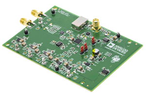
Analog Devices Inc.DC1233A-D: Demo Board for LT5579 1.5GHz to 3.8GHz High Linearity Upconverting Mixer.
LTC6601-2 | Low Power, Low Distortion Configurable Broadband Filter Demo Board
Analog Devices Inc.DC1251A-B: Demo Board for LTC6601-2 - Low Power, Low Distortion, Low Power, Low Distortion, 5MHz to 27MHz, Pin Configurable Filter/ADC Driver
DC1255A-A
Analog Devices Inc.The LTC1605 is a 100ksps, sampling 16-bit A/D converter that draws only 55mW (typical) from a single 5V supply. This easy-to-use device includes sample-and-hold, precision reference, switched capacitor successive approximation A/D and trimmed internal clock.The LTC1605?s input range is an industry standard ?10V. Maximum DC specs include ?2.0LSB INL and 16-bits no missing codes over temperature. An external reference can be used if greater accuracy over temperature is needed.The ADC has a microprocessor compatible, 16-bit or two byte parallel output port. A convert start input and a data ready signal (BUSY) ease connections to FIFOs, DSPs and microprocessors. Input Voltage Range LTC1605 Bipolar ?10V LTC1605-1 Unipolar 0V to 4V LTC1605-2 Bipolar ?4V Applications Industrial Process Control Multiplexed Data Acquisition Systems High Speed Data Acquisition for PCs Digital Signal Processing
LTC2453 16-bit I2C Differential ADC in 3x2 DFN (requires DC590)
Analog Devices Inc.DC1266A-A: Demo Board for the LTC2453 Ultra-Tiny, Differential, 16-Bit ∆Σ ADC With I2C Interface
LTC3125EDCB Demo Board | 1.5A Switch, 3.3V Input, VOUT = 4V @ 500mA (2A Pulses)
Analog Devices Inc.Demonstration circuit 1267A is a step-up DC/DC regulator featuring the LTC3125EDCB and is ideally suited for pulsed load applications where the input current needs to be limited. Demonstration circuit 1267A is configured for 500mA maximum input current limit and can handle pulsed load currents of up to 2A, with duty cycles of up to 15%. The input voltage range is 3.3V ±10%.
DC126A
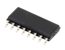
Analog Devices Inc.The LTC1520 is a high speed, precision differential line receiver that can operate at data rates as high as 50Mbps. A unique architecture provides very stable propagation delays and low skew over a wide input common mode, input overdrive and ambient temperature range. Propagation delay is 18ns ?3ns, while typically tPLH/tPHL skew is 500ps and channel-to-channel skew is 400ps.Each receiver translates differential input levels (VID ? 100mV) into valid CMOS and TTL output levels. Its high input resistance (?18k) allows many receivers to be connected to the same driver. The receiver outputs go into a high impedance state when disabled.Protection features include thermal shutdown and a controlled maximum short-circuit current (50mA max) that does not oscillate in and out of short-circuit mode. Input resistance remains ?18k when the device is unpowered or disabled, thus allowing the LTC1520 to be hot swapped into a backplane without loading the data lines.The LTC1520 operates from a single 5V supply and draws 12mA of supply current. The part is available in a 16-lead narrow SO package.Applications High Speed Backplane Interface Line Collision Detector PECL and LVDS Line Receivers Level Translator Ring Oscillator Tapped Delay Line
LT1938EDD | 25V. 2.2A, 2.8MHz Step-Down Switching Regulator
Analog Devices Inc.DC1273A: Demo Board for LT1938 - 25V, 2.2A, 2.8MHz Step-Down Switching Regulator
LT3080EDD Demo Board | LT3080(x4), Paralleled, Single Resistor LDOs, 3.8V ≤ VIN ≤ 25V, VOUT = 3.3V @ 4.4A
Analog Devices Inc.Demonstration circuit 1294A exercises four adjustable linear regulators in parallel using the LT3080. A small 20 mΩ ballast resistor is required for parallel operation. A short PCB trace can easily serve that purpose. The paralleled devices provide up to 4.4A of output current at 3.3V.
Architected as a precision current source and voltage follower, the LT3080 can be used in many applications requiring high current, adjustability to zero output, and no heat sink. The device brings out the collector of the pass transistor to allow low dropout operation when used with multiple supplies. The LT3080's output voltage can be programmed to any level between 0V and 36V; however the demo board has a reduced input voltage range from 3.8V to 25V due to the input capacitor voltage rating.
LTM4612EV Demo Board | EN55022B Compliant, 5V ≤ VIN ≤ 36V, VOUT = 3.3V or 5V @ 5A, or VOUT = 12V @ 3A
Analog Devices Inc.Demonstration circuit DC1297B features the LTM4612EV, an EN55022 Class B certified synchronous step-down power module. The board accepts an input voltage from 5V to 36V and delivers a jumper programmable output voltage of 3.3V, 5V or 12V. The rated load current is 5A for 3.3V and 5V output voltages, or 3A for a 12V output. Current derating is necessary for certain VIN, VOUT, and thermal conditions.
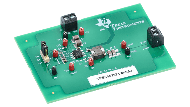
Evaluation Module for TPS54528 Synchronous Step-Down Converter with D-CAP2 Mode & Auto-Skip
Texas InstrumentsEvaluation Module for TPS54528 Synchronous Step-Down Converter with D-CAP2 Mode & Auto-Skip
BQ24012 1-A Li-Ion Charger Evaluation Module w/ Power-Good; Charge Enable
Texas InstrumentsBQ24012 1-A Li-Ion Charger Evaluation Module w/ Power-Good; Charge Enable
N-Channel Controller for Dimmable LED Drives with Low-Side Current Sense Evaluation Module Board
Texas InstrumentsN-Channel Controller for Dimmable LED Drives with Low-Side Current Sense Evaluation Module Board


