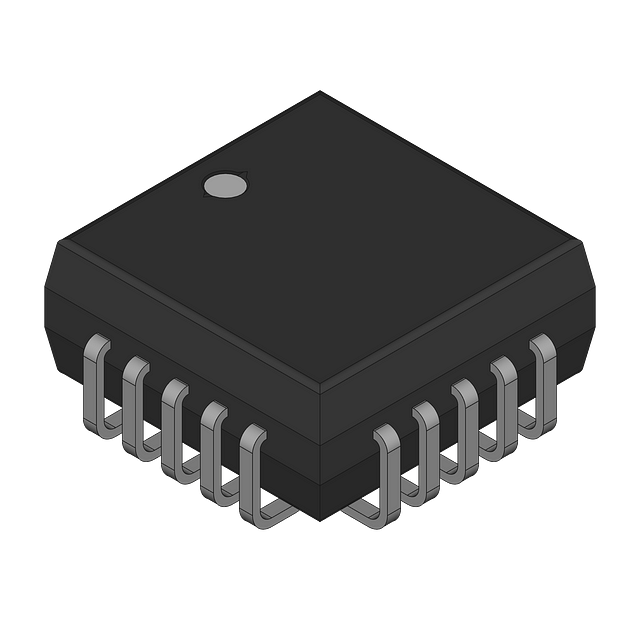
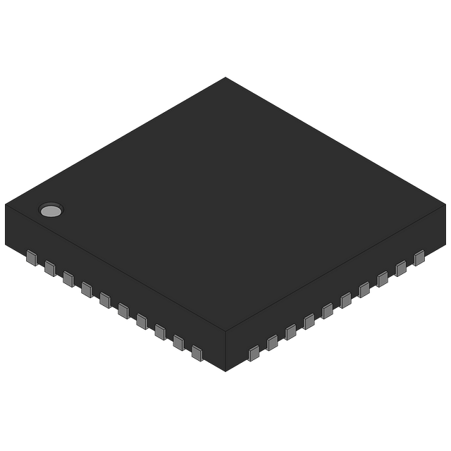
AD9549A/PCBZ
Analog Devices Inc.The AD9549 provides synchronization for many systems, including synchronous optical networks (SONET/SDH). The AD9549 generates an output clock, synchronized to one of two external input references. The external references may contain significant time jitter, also specified as phase noise. Using a digitally controlled loop and holdover circuitry, the AD9549 continues to generate a clean (low jitter), valid output clock during a loss of reference condition, even when both references have failed.The AD9549 operates over an industrial temperature range of ?40?C to +85?C.APPLICATIONS Network synchronization Reference clock jitter cleanup SONET/SDH clocks up to OC-192, including FEC Stratum 3/3E reference clocks Wireless base stations, controllers Cable infrastructure Data communications
AD9550/PCBZ
Analog Devices Inc.The AD9550 is a phase-locked loop (PLL) based clock translatordesigned to address the needs of wireline communicationand base station applications. The device employs an integer-NPLL to accommodate the applicable frequency translationrequirements. It accepts a single-ended input reference signalat the REF input.The AD9550 is pin programmable, providing a matrix ofstandard input/output frequency translations from a list of15 possible input frequencies to a list of 51 possible outputfrequency pairs (OUT1 and OUT2).The AD9550 output is compatible with LVPECL, LVDS, orsingle-ended CMOS logic levels, although the AD9550 isimplemented in a strictly CMOS process.The AD9550 operates over the extended industrial temperaturerange of ?40?C to +85?C.APPLICATIONS Cost effective replacement of high frequency VCXO, OCXO, and SAW resonators Flexible frequency translation for wireline applications such as Ethernet, T1/E1, SONET/SDH, GPON, xDSL Wireless infrastructure Test and measurement (including handheld devices)
AD9554/PCBZ
Analog Devices Inc.The AD9554 is a low loop bandwidth clock translator that provides jitter cleanup and synchronization for many systems, including synchronous optical networks (SONET/SDH). The AD9554 generates an output clock synchronized to up to four external input references. The digital PLL (DPLL) allows for reduction of input time jitter or phase noise associated with the external references. The digitally controlled loop and holdover circuitry of the AD9554 continuously generates a low jitteroutput clock even when all reference inputs have failed.The AD9554 operates over an industrial temperature range of ?40?C to +85?C. If a smaller device is needed, the AD9554-1 is a version of this device with one output per PLL. If a single or dual DPLL version of this device is needed, refer to the AD9557 or AD9559, respectively.Applications Network synchronization, including synchronous Ethernet and synchronous digital hierarchy (SDH) to optical transport network (OTN) mapping/demapping Cleanup of reference clock jitter SONET/SDH clocks up to OC-192, including FEC Stratum 3 holdover, jitter cleanup, and phase transient control Cable infrastructure Data communications Professional video
EVAL-AD7794EBZ
Analog Devices Inc.The AD7794/AD7795 are low power, low noise, complete analog front ends for high precision measurement applications. They contain a low noise, 24-/16-bit ?-? ADC with six differential inputs. The on-chip low noise instrumentation amplifier means that signals of small amplitude can be interfaced directly to the ADC.Each device contains a precision, low noise, low drift internal band gap reference, and can also accept up to two external differential references. Other on-chip features include programmable excitation current sources, burnout currents, and a bias voltage generator that is used to set the common-mode voltage of a channel to AVDD/2. The low-side power switch can be used to power down bridge sensors between conversions, minimizing the system?s power consumption. The AD7794/AD7795 can operate with either an internal clock or an external clock. The output data rate from each part can vary from 4.17 Hz to 470 Hz.Both parts operate with a power supply from 2.7 V to 5.25 V. The B-grade parts (AD7794 and AD7795) are specified for a temperature range of ?40?C to +105?C while the C-grade part (AD7794) is specified for a temperature range of ?40?C to +125?C. They consume a current of 400 ?A typical and are housed in a 24-lead TSSOP.Applications Temperature measurement Pressure measurement Weigh scales Strain gage transducers Gas analysis
104130-HMC596LP4
Analog Devices Inc.The HMC596LP4(E) is a low-cost 4x2 switch matrix in a leadless QFN 4x4 mm surface mount package for use in Satellite/DBS, LNBs and multiswitches from 200 to 3000 MHz. A positive voltage controlled 4 bit decoder is integrated on the switch. The switches may be used in either 75 ohm or 50 ohm systems.Both switch outputs (OP1 & OP2) can independently select any of the four inputs (HH, HL, VH, VL) or simultaneously select the same inputs. Note that the switch is bi-directional and input/output functionality may be interchanged. All data presented was measured in a 50 ohm (input/output) system.APPLICATIONS DBS LNBs & Multiswitches Cable Modem/CATV Cellular Systems
104356-HMC326MS8G
Analog Devices Inc.The HMC326MS8G & HMC326MS8GE are high efficiency GaAs InGaP Heterojunction Bipolar Transistor (HBT) MMIC driver amplifiers which operate between 3.0 and 4.5 GHz. The amplifier is packaged in a low cost, surface mount 8 leaded package with an exposed base for improved RF and thermal performance. The amplifier provides 21 dBof gain and +26 dBm of saturated power from a +5V supply voltage. Power down capability is available to conserve current consumption when the amplifier is not in use. Internal circuit matching was optimized to provide greater than 40% PAE.Applications Microwave Radios Broadband Radio Systems Wireless Local Loop Driver Amplifier
105006-HMC414MS8G
Analog Devices Inc.The HMC414MS8G(E) is a high efficiency GaAs InGaP Heterojunction Bipolar Transistor (HBT) MMIC Power amplifier which operates between 2.2 and 2.8 GHz. The amplifier is packaged in a low cost, surface mount 8 leaded package with an exposed base for improved RF and thermal performance. With a minimum of external components, the amplifier provides 20 dB of gain, +30 dBm of saturated power at 32% PAE from a +5V supply voltage. The amplifier can also operate with a 3.6V supply. Vpd can be used for full power down or RF output power/ current control.Applications BLUETOOTH MMDS
105706-HMC385LP4
Analog Devices Inc.The HMC385LP4(E) is a GaAs InGaP Heterojunction Bipolar Transistor (HBT) MMIC VCO with integrated resonator, negative resistance device, varactor diode, and buffer amplifier. Covering 2.25 to 2.5 GHz, the VCO?s phase noise performance is excellent over temperature, shock, vibration and process due to the oscillator?s monolithic structure. Power output is 4.5 dBm typical from a single supply of 3V @ 35mA. The voltage controlled oscillator is packaged in a low cost leadless QFN 4x4 mm surface mount package.APPLICATIONS Wireless Infrastructure Industrial Controls Test Equipment Military
105786-HMC437MS8G
Analog Devices Inc.The HMC437MS8G(E) is a low noise Divide-by-3 Static Divider utilizing InGaP GaAs HBT technology in a low cost 8 lead surface mount plastic package. This device operates from DC (with a square wave input) to 7 GHz input frequency from a single +5V DC supply. The low additive SSB phase noise of -153 dBc/Hz at 100 kHz offset helps the user maintain good system noise performance.APPLICATIONS UNII, Point-to-Point & VSAT Radios 802.11a & HiperLAN WLAN Fiber Optic Cellular/3G Infrastructure
105811-HMC440QS16G
Analog Devices Inc.The HMC440QS16G(E) is an integer-n synthesizer that incorporates a 10 to 1300 MHz digital Phase-Frequency Detector with 10 to 2800 MHz 5-Bit frequency counter (continuous division from 2 to 32) in miniature 16 lead QSOP plastic packages. It is intended for use in low phase noise offset-synthesizer app-lications.The HMC440QS16G(E) combines high frequency operation along with ultra low phase noise floor making possible synthesizers with wide loop bandwidth and low N resulting in fast settling and very low phase noise. When used in conjunction with a differential loop amplifier, the HMC440QS16G(E) generates an output voltage that can be used to phase lock a VCO to a reference oscillator.Applications Satellite Communication Systems? Point-to-Point Radios? Military Applications? Sonet Clock Generation Test Equipment
EVAL-ADF7021-NDBEZ
Analog Devices Inc.The ADF7021-N is a high performance, low power, narrow-band transceiver based on the ADF7021. The ADF7021-N has IF filter bandwidths of 9 kHz, 13.5 kHz, and 18.5 kHz, making it ideally suited to worldwide narrowband standards and particularly those that stipulate 12.5 kHz channel separation. It is designed to operate in the narrow-band, license-free ISM bands and in the licensed bands with frequency ranges of 80 MHz to 650 MHz and 842 MHz to 916 MHz. The part has both Gaussian and raised cosine transmit data filtering options to improve spectral efficiency for narrow-band applications. It is suitable for circuit applications targeted at the Japanese ARIB STD-T67, the European ETSI EN 300 220, the Korean short range device regulations, the Chinese short range device regulations, and the North American FCC Part 15, Part 90, and Part 95 regulatory standards. A complete transceiver can be built using a small number of external discrete components, making the ADF7021-N very suitable for price-sensitive and area-sensitive applications. The range of on-chip FSK modulation and data filtering options allows users greater flexibility in their choice of modulation schemes while meeting the tight spectral efficiency requirements. The ADF7021-N also supports protocols that dynamically switch among 2FSK, 3FSK, and 4FSK to maximize communica-tion range and data throughput. The transmit section contains two voltage controlled oscillators (VCOs) and a low noise fractional-N PLL with an output resolution of The frequency-agile PLL allows the ADF7021-N to be used in frequency-hopping, spread spectrum (FHSS) systems. Both VCOs operate at twice the fundamental frequency to reduce spurious emissions and frequency pulling problems. The transmitter output power is programmable in 63 steps from ?16 dBm to +13 dBm and has an automatic power ramp control to prevent spectral splatter and help meet regulatory standards. The transceiver RF frequency, channel spacing, and modulation are programmable using a simple 3-wire interface. The device operates with a power supply range of 2.3 V to 3.6 V and can be powered down when not in use. A low IF architecture is used in the receiver (100 kHz), which minimizes power consumption and the external component count yet avoids dc offset and flicker noise at low frequencies. The IF filter has programmable bandwidths of 9 kHz, 13.5 kHz, and 18.5 kHz. The ADF7021-N supports a wide variety of pro-grammable features including Rx linearity, sensitivity, and IF bandwidth, allowing the user to trade off receiver sensitivity and selectivity against current consumption, depending on the application. The receiver also features a patent-pending automatic frequency control (AFC) loop with programmable pull-in range that allows the PLL to track out the frequency error in the incoming signal. The receiver achieves an image rejection performance of 56 dB using a patent-pending IR calibration scheme that does not require the use of an external RF source. An on-chip ADC provides readback of the integrated tempera-ture sensor, external analog input, battery voltage, and RSSI signal, which provides savings on an ADC in some applications. The temperature sensor is accurate to ?10?C over the full oper-ating temperature range of ?40?C to +85?C. This accuracy can be improved by performing a 1-point calibration at room temperature and storing the result in memory.
LTC7050/LTC3884-1 2-Phase, Dual-Output Synchronous Buck Converter with Power System Management
Analog Devices Inc.Demonstration circuit 2881A-A is a 2-phase dual-output, high efficiency, high density, synchronous buck converter with 7V to 14V input range. Each output can supply up to 30A maximum load current with 1V output. The demo board features the LTC3884-1 controller paired with the LTC7050 dual smart power stage to provide a 2-phase buck converter solution. The LTC3884-1 is a dual output poly phase step-down controller with digital power system management. The LTC7050 is a dual monolithic smart power stage which integrates high speed drivers with low resistance half-bridge power switches plus comprehensive monitoring and protection circuitry in an electrically and thermally optimized package. Please refer to the LTC3884-1 and LTC7050 data sheet for more detailed information.
DC2881A-A powers up to default settings and produces power based on configuration resistors (or with the setting in its non-volatile memory) without the need for any serial bus communication. This allows easy evaluation of the DC/DC converter. To fully explore the extensive power system management features of the part, download the GUI software LTpowerPlay® onto your PC and use ADI’s I2C/SMBus/PMBus dongle DC1613A to connect to the board. LTpowerPlay allows the user to reconfigure the part on the fly and store the configuration in EEPROM, view telemetry of voltage, current, temperature and fault status.
ADL5387-EVALZ
Analog Devices Inc.The ADL5387 is a broadband quadrature I/Q demodulator that covers an RF/IF input frequency range from 30 MHz to 2 GHz. With a NF = 13.2 dB, IP1dB = 12.7 dBm, and IIP3 = 32 dBm @ 450 MHz, the ADL5387 demodulator offers outstanding dynamic range suitable for the demanding infrastructure direct-conversion requirements. The differential RF/IF inputs provide a well-behaved broadband input impedance of 50 ? and are best driven from a 1:1 balun for optimum performance.Ultrabroadband operation is achieved with a divide-by-2 method for local oscillator (LO) quadrature generation. Over a wide range of LO levels, excellent demodulation accuracy is achieved with amplitude and phase balances ~0.05 dB and ~0.4?, respectively. The demodulated in-phase (I) and quadrature (Q) differential outputs are fully buffered and provide a voltage conversion gain of >4 dB. The buffered baseband outputs are capable of driving a 2 Vp-p differential signal into 200 ?.The fully balanced design minimizes effects from second-order distortion. The leakage from the LO port to the RF port is 60 dBm.The ADL5387 operates off a single 4.75 V to 5.25 V supply. The supply current is adjustable with an external resistor from the BIAS pin to ground.The ADL5387 is fabricated using the Analog Devices, Inc. advanced silicon-germanium bipolar process and is available in a 24-lead exposed paddle LFCSP.APPLICATIONS QAM/QPSK RF/IF demodulators W-CDMA/CDMA/CDMA2000/GSM Microwave point-to-(multi)point radios Broadband wireless and WiMAX Broadband CATVs
ADZS-A2B-ANALYZER
Analog Devices Inc.The Automotive Audio Bus? (A2B?) is an innovative technology that reduces system cost, weight, and design complexity by distributing audio and control data, together with clock and power over a single, low-cost, unshielded twisted pair cable. The AD2425W is an enhanced A2B transceiver offering an expanded feature set while retaining complete compatibility with existing AD241x devices. The AD2425W is fully configurable supporting both master and slave functionality.The AD2425W is targeted for use in wiring intensive applications where reducing the weight or complexity of existing cable harnesses is a primary system design objective. These applications include Premium Audio Systems, Active Noise Cancellation, and In-Car Communications.Applications Automotive audio communication link Active noise cancellation Microphone arrays for hands free and in car communication
LT8365 Demo Board | Low IQ Boost/SEPIC/Inverting Regulator with 150V, 1.5A Switch
Analog Devices Inc.Demonstration circuit 2838A features the LT8365 in a boost configuration. It operates with a switching frequency of 400kHz and is designed to convert a 9V to 30V source to 250V, with 10mA output current.
The demo board contains an optional third charge pump stage for applications requiring higher output voltages. If needed, remove R14 and install optional components. Output voltage sensing connections remain the same.
The LT8365 can be used for different topologies with input voltages up to 60V. However, component selection in this demo circuit restricts the input voltage to 30V.
The demo board contains a selectable jumper, JP1, to aid in the selection of the desired sync pin mode of operation. The default setting is Burst Mode® operation.
This layout is optimized for good EMI performance and small solution size. Input and output filters are necessary for CISPR 25 Class 5 emissions. Radiated emissions plots are included in this manual.
The data sheet gives a complete description of the device, operation and application information. The data sheet must be read in conjunction with this demo manual.
LTM4660 | High Density Hybrid Step-Down Synchronous Converter
Analog Devices Inc.Demonstration circuit 2879A is a high efficiency, high power density hybrid converter. It can deliver 12V/25A with an input voltage from 36V to 60V (up to 65V during transients). This demo board features the LTM4660, which uses an architecture that merges soft-switching switched capacitor topology with a traditional step-down converter to provide superior efficiency compared to the traditional switching architectures. It offers a high efficiency/high density and cost effective solution for nonisolated intermediate bus applications in power distribution, datacom and telecom.
Due to its current mode control architecture, multiple LTM4660s can be operated in a parallel, multiphase configuration with excellent current sharing and low output voltage ripple to enable much higher power applications. Other benefits include low EMI emissions due to a soft-switched front end and reduced MOSFET stress.
The LTM4660 design eliminates the inrush current typically associated with switched capacitor circuits by pre-balancing the capacitors on start-up. The LTM4660 also monitors system voltage, current and temperature for faults. It stops switching and pulls the FAULT pin low when a fault condition occurs. An onboard timer can be set for appropriate restart/retry times.
Additional features include ±1.5% output voltage accuracy over temperature, a clock output for multiphase operation, a power good output signal, short-circuit protection, monotonic output voltage start-up, optional external reference, undervoltage lockout and internal charge balance circuitry.
The LTM4660 data sheet must be used in conjunction with this demo board manual.
LTC5536ES6 | RF Power Detector With Output Comparator
Analog Devices Inc.DC730A: Demo Board for the LTC5536 600MHz to 7GHz Precision RF Detector with Fast Comparator Output.


