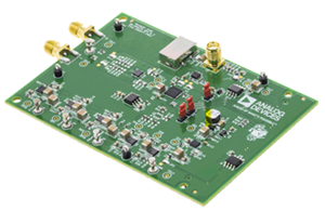
ADCLK914/PCBZ
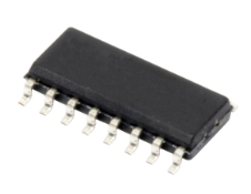
Analog Devices Inc.The ADCLK914 is an ultrafast clock/data buffer fabricated onthe Analog Devices, Inc., proprietary, complementary bipolar(XFCB-3) silicon-germanium (SiGe) process. The ADCLK914features high voltage differential signaling (HVDS) outputssuitable for driving the latest Analog Devices high speed digitalto-analogconverters (DACs). The ADCLK914 has a single,differential open-collector output.The ADCLK914 buffer operates up to 7.5 GHz with a 160 pspropagation delay and adds only 110 fs random jitter (RJ).The input has a center tapped, 100 ?, on-chip terminationresistor and accepts LVPECL, CML, CMOS, LVTTL, or LVDS(ac-coupled only). A VREF pin is available for biasing ac-coupledinputs.The HVDS output stage is designed to directly drive 1.9 V eachside into 50 ? terminated to VCC for a total differential outputswing of 3.8 V.The ADCLK914 is available in a 16-lead LFCSP. It is specifiedfor operation over the extended industrial temperature range of?40?C to +125?C.Applications Clock and data signal restoration High speed converter clocking Broadband communications Cellular infrastructure High speed line receivers ATE and high performance instrumentation Level shifting Threshold detection?
ADCMP380-EVALZ
Analog Devices Inc.The ADCMP380 is an ultralow power voltage comparator with internal reference suitable for use in general-purpose applications. The ultralow power consumption of this device makes it suitable for power efficiency sensitive systems, such as battery-powered portable devices and energy meters.The ADCMP380 is available with a 0.5 V and 1 V internal reference with ?2.2% and ?1.6% accuracy, respectively, over the full temperature range; this internal reference enables the device to monitor the node of interest accurately to 0.5 V. The enable input allows the user to hold the output low regardless of thestate of the input.The ADCMP380 is available in a 6-ball, 1.46 mm ? 0.96 mm WLCSP and is specified over the temperature range of ?40?C to +85?C.APPLICATIONS Portable/battery-operated equipment Battery monitors Energy harvesting
ADCMXL_BRKOUT/PCBZ
Analog Devices Inc.The ADcmXL3021 is a complete vibration sensing system that combines high performance vibration sensing (using micro-electromechanical systems (MEMS) accelerometers) with a variety of signal processing functions to simplify the development of smart sensor nodes in condition-based monitoring (CBM) systems. The typical ultralow noise density (26 ?g/?Hz) in the MEMS accelerometers supports excellent resolution. The wide bandwidth (dc to 10 kHz within 3 dB flatness) enables tracking of key vibration signatures on many machine platforms.The signal processing includes high speed data sampling (220 kSPS), 4096 time sample record lengths, filtering, windowing, fast Fourier transform (FFT), user configurable spectral or time statistic alarms, and error flags. The serial peripheral interface (SPI) provides access to a register structure that contains the vibration data and a wide range of user configurable functions.The ADcmXL3021 is available in a 23.7 mm ? 27.0 mm ? 12.4 mm aluminum package with four mounting flanges to support installation with standard machine screws. This package provides consistent mechanical coupling to the core sensors over a broad frequency range. The electrical interface is through a 14-pin connector on a 36 mm flexible cable, which enables a wide range of location and orientation options for system mating connectors.The ADcmXL3021 requires only a single, 3.3 V power supply and supports an operating temperature range of ?40?C to +105?C.Applications Vibration analysis CBM systems Machine health Instrumentation and diagnostics Safety shutoff sensing
ADD5211EB-EVALZ
Analog Devices Inc.The ADD5211 is a four-string, white LED driver for backlight applications based on high efficiency, current mode, step-up converter technology. The boost controller drives an external MOSFET switch for step-up regulation from an input voltage of 4.5 V to 40 V and a pin adjustable operating frequency from 200 kHz to 1.2 MHz. An adjustable UVLO function is implemented to reduce input current during power-off.The ADD5211 provides four regulated current sinks for uniform brightness intensity. Each current sink can be driven from 40 mA to 200 mA; the LED driving current is pin adjustable using an external resistor. With an input PWM interface, the ADD5211 drives up to four parallel strings of multiple series connected LEDs.Additional features include LED short protection, LED open protection, boost output short protection, overvoltage protection, cycle-by-cycle current limit, and thermal shutdown for both the IC and the LED array. An open-drain fault output is also included. A programmable soft start is implemented to reduce inrush current during startup. Applications LCD monitor and TV LED backlights Industrial lighting
ADF70301-868EZKIT
Analog Devices Inc.The ADF7030-1 is a fully integrated, radio transceiver achieving high performance at very low power. The ADF7030-1 is ideally suited for applications that require long range, network robustness, and long battery life. It is suitable for applications that operate in the ISM, SRD, and licensed frequency bands at 169.4 MHz to 169.6 MHz, 426 MHz to 470 MHz, and 863 MHz to 960 MHz. It provides extensive support for standards-based protocols like IEEE802.15.4g while also providing flexibility to support a wide range of proprietary protocols.The highly configurable low intermediate frequency (IF) receiver supports a large range of receiver channel bandwidths from 2.6 kHz to 406 kHz. This range of receiver channel bandwidths allows the ADF7030-1 to support ultranarrow-band, narrow-band, and wideband channel spacing.The ADF7030-1 features two independent PAs supporting output power ranges of ?20 dBm to +13 dBm and ?20 dBm to +17 dBm. The PAs support ultrafine adjustment of the power with a step resolution of 0.1 dB. The PA output power is exceptionally robust over temperature and voltage. The PAs have an automatic power ramp control to limit spectral splatter to meet regulatory standards.The ADF7030-1 features an on-chip ARM??Cortex?-M0 processor that performs radio control, radio calibration, and packet management. Cortex-M0 eases the processing burden of the host processor because the ADF7030-1 integrates the lower layers of a typical communication protocol stack. This internal processor also permits the download and execution of Analog Devices, Inc., provided firmware modules that can extend the functionality of the ADF7030-1.The ADF7030-1 has two packet modes: generic packet mode and IEEE802.15.4g mode. In generic packet mode, the packet format is highly flexible and fully programmable, thereby ensuring its compatibility with proprietary packet formats. In IEEE802.15.4g packet mode, the packet format conforms to the?IEEE802.15.4g standard. FEC, as per the IEEE802.15.4g standard, is also supported.The ADF7030-1 operates with a power supply range of 2.2 V to 3.6 V and has very low power consumption in both Tx and Rx modes, enabling long lifetimes in battery-operated systems. An ultralow power deep sleep mode achieves a typical current of 10 nA with the configuration memory retained.A complete wireless solution can be built using a small number of external discrete components and a host processor (typically a microcontroller). The host processor can configure the ADF7030-1 using a simple command-based protocol over a standard 4-wire SPI interface. A single-byte command transitions the radio between states or performs a radio function.The ADF7030-1 is available in two package types: a 6 mm ? 6 mm, 40-lead LFCSP and a 7 mm ? 7 mm, 48-lead LQFP. Both package types use NiPdAu plating to mitigate against silver migration in high humidity applications. The ADF7030-1 operating temperature range is ?40?C to +85?C.For Figure 13 to Figure 19, Figure 30, Figure 42, Figure 60, Figure 61, and Figure 75 in the Typical Performance Characteristics section, PA_COARSE is a programmable value that provides a coarse adjustment of the PA output power. This value can be programmed in the range of 1 to 6 for PA1, and from 1 to 10 for PA2. PA_FINE is a programmable value that provides a fine adjustment of the PA output power. This value can be programmed in the range of 3 to 127 for both PA1 and PA2. PA_MICRO is a programmable value that provides a microadjustment (typically
ADL5243-EVALZ
Analog Devices Inc.The ADL5243 is a high performance, digitally controlled variable gain amplifier operating from 100 MHz to 4000 MHz.The VGA integrates two high performance amplifiers and a digital step attenuator (DSA). Amplifier 1 (AMP1) is an internally matched gain block amplifier with 20 dB gain, and Amplifier 2 (AMP2) is a broadband ? W driver amplifier that requires very few external tuning components. The DSA is 6-bit with a 31.5 dB gain control range, 0.5 dB steps, and ?0.25 dB step accuracy. The attenuation of the DSA can be controlled using a serial or parallel interface.The gain block and DSA are internally matched to 50 ? at their inputs and outputs, and all three internal devices are separately biased. The separate bias allows all or part of the ADL5243 to be used, which allows for easy reuse throughout a design. The pinout of the ADL5243 also enables the gain block, DSA, or ? W driver amplifier to be first, giving the VGA maximum flexibility in a signal chain.The ADL5243 consumes 175 mA and operates off a single supply ranging from 4.75 V to 5.25 V. The VGA is packaged in a thermally efficient, 5 mm ? 5 mm, 32-lead LFCSP and is fully specified for operation from ?40?C to +85?C. A fully populated evaluation board is available.ApplicationsWireless infrastructureAutomated test equipmentRF/IF gain control
ADL5370-EVALZ
Analog Devices Inc.The ADL5370 is the first in the fixed-gain quadrature modulator(F-MOD) family designed for use from 300 MHz to 1000 MHz.Its excellent phase accuracy and amplitude balance enable highperformance intermediate frequency or direct radio frequencymodulation for communication systems.The ADL5370 provides a greater than 500 MHz, 3 dB basebandbandwidth, making it ideally suited for use in broadband zeroIF or low IF-to-RF applications and in broadband digitalpredistortion transmitters.The ADL5370 accepts two differential baseband inputs and asingle-ended LO and generates a single-ended 50 ? output.The ADL5370 is fabricated using the Analog Devices, Inc.advanced silicon-germanium bipolar process. It is available in a24-lead, exposed-paddle, Pb-free, LFCSP package. Performance isspecified over a ?40?C to +85?C temperature range. A Pb-freeevaluation board is available.Applications Cellular communication systems at 450 MHz CDMA2000/GSM WiMAX/broadband wireless access systems Cable communication equipment Satellite modems
ADL5375-15-EVALZ
Analog Devices Inc.The ADL5375 is a broadband quadrature modulator designed for operation from 400 MHz to 6 GHz. Its excellent phase accuracy and amplitude balance enable high performance intermediate frequency or direct radio frequency modulation for communication systems.The ADL5375 features a broad baseband bandwidth, along with an output gain flatness that varies no more than 1 dB from 450 MHz to 3.8 GHz. These features, coupled with a broadband output return loss of
ADL5380-EVALZ
Analog Devices Inc.The ADL5380 is a broadband quadrature I-Q demodulator that covers an RF/IF input frequency range from 400 MHz to 6 GHz. With a NF = 10.9 dB, IP1dB = 11.6 dBm, and IIP3 = 29.7 dBm @ 900 MHz, the ADL5380 demodulator offers outstanding dynamic range suitable for the demanding infrastructure direct-conversion requirements. The differential RF inputs provide a well-behaved broadband input impedance of 50 ? and are best driven from a 1:1 balun for optimum performance.Excellent demodulation accuracy is achieved with amplitude and phase balances of ~0.07 dB and ~0.2?, respectively. The demodulated in-phase (I) and quadrature (Q) differential outputs are fully buffered and provide a voltage conversion gain of ~7 dB. The buffered baseband outputs are capable of driving a 2 Vp-p differential signal into 200 ?.The fully balanced design minimizes effects from second-order distortion. The leakage from the LO port to the RF port is 65 dBm.The ADL5380 operates off a single 4.75 V to 5.25 V supply. The supply current is adjustable by placing an external resistor from the ADJ pin to either the positive supply, VS, (to increase supply current and improve IIP3) or to ground (which decreases supply current at the expense of IIP3).The ADL5380 is fabricated using the Analog Devices, Inc., advanced silicon-germanium bipolar process and is available in a 24-lead exposed paddle LFCSP.APPLICATIONS Cellular W-CDMA/GSM/LTE Microwave point-to-(multi)point radios Broadband wireless and WiMAX
ADL5391-EVALZ
Analog Devices Inc.The ADL5391 draws on three decades of experience in advanced analog multiplier products. It provides the same general mathematical function that has been field proven to provide an exceptional degree of versatility in function synthesis:VW?= ? ? (VX?x VY)/1 V + VZThe most significant advance in the ADL5391 is the use of anew multiplier core architecture, which differs markedly fromthe conventional form that has been in use since 1970. Theconventional structure that employs a current mode, translinearcore is fundamentally asymmetric with respect to the X and Yinputs, leading to relative amplitude and timing misalignmentsthat are problematic at high frequencies. The new multiplier coreeliminates these misalignments by offering symmetric signalpaths for both X and Y inputs. The Z input allows a signal to beadded directly to the output. This can be used to cancel a carrieror to apply a static offset voltage.The fully differential X, Y, and Z input interfaces are operationalover a ?2 V range, and they can be used in single-ended fashion.The user can apply a common mode at these inputs to varyfrom the internally set VPOS/2 down to ground. If these inputsare ac-coupled, their nominal voltage will be VPOS/2. These inputinterfaces each present a differential 500 ? input impedance up toapproximately 700 MHz, decreasing to 50 ? at 2 GHz. The gainscaling input, GADJ, can be used for fine adjustment of the gainscaling constant (?) about unity.The differential output can swing ?2 V about the VPOS/2common-mode and can be taken in a single-ended fashion aswell. The output common mode is designed to interface directlyto the inputs of another ADL5391. Light dc loads can be groundreferenced; however, ac-coupling of the outputs is recommendedfor heavy loads.The ENBL pin allows the ADL5391 to be disabled quickly to astandby mode. It operates off supply voltages from 4.5 V to 5.5 Vwhile consuming approximately 130 mA.The ADL5391 is fabricated on Analog Devices, Inc. proprietary,high performance, 65 GHz, SOI complementary, SiGe bipolarIC process. It is available in a 16-lead, RoHS compliant, LFCSPand operates over a ?40?C to +85?C temperature range.Evaluation boards are available.Applications Wideband multiplication and summing High frequency analog modulation Adaptive antennas (diversity/phased array) Square-law detectors and true rms detectors Accurate polynomial function synthesis DC capable VGA with very fast control
ADL5502-EVALZ
Analog Devices Inc.The ADL5502 is a mean-responding (true rms) power detector incombination with an envelope detector to accurately determinethe crest factor of a modulated signal. It can be used in highfrequency receiver and transmitter signal chains from 450 MHzto 6 GHz with envelope bandwidths over 10 MHz. Requiringonly a single supply between 2.5 V and 3.3 V, the detector drawsless than 3 mA. The input is internally ac-coupled and has anominal input impedance of 500 ?.The rms output is a linear-responding dc voltage with aconversion gain of 1.8 V/V rms at 900 MHz. The peak envelopeoutput with a conversion gain of 1.2 V/V is toggledfor peak hold with less than 1% output voltage droop in over 1 ms.The ADL5502 is a highly accurate, easy to use means ofdetermining the rms and peak to the average value of complex waveforms.It can be used for crest factor measurements of both simple andcomplex waveforms but is particularly useful for measuringhigh crest factor (high peak-to-rms ratio) signals, such as W-CDMA,CDMA2000, and QPSK-/QAM-based OFDMwaveforms. The peak hold function allows the capture of shortpeaks in the envelope with lower sampling rate ADC?s.The crest factor detector operates from ?40?C to +85?C and isavailable in an 8-ball, 1.5 mm ? 1.5 mm wafer-level chip scalepackage. It is fabricated on a high fT silicon BiCMOS process.ApplicationsPower and envelope measurement of W-CDMA, CDMA2000,and QPSK-/QAM-based OFDM, and other complex modulation waveformsRF transmitter or receiver power and envelope measurement
ADL5506-EVALZ
Analog Devices Inc.The ADL5506 is a complete, low cost subsystem for the measurement of RF signals in the 30 MHz to 4.5 GHz frequency range, with a typical dynamic range of 45 dB, intended for use in a wide variety of wireless terminal devices. It provides a wider dynamic range and better accuracy than is possible using discrete diode detectors. In particular, its temperature stability is excellent over ?40?C to +85?C.Its high sensitivity allows measurement of low power levels, thus reducing the amount of power that needs to be coupled to the detector. It is essentially a voltage responding device, with a typical dynamic range of 45 dB.For convenience, the signal is internally ac-coupled, using a 5 pF capacitor and a broadband 50 ? match, with an external shunt resistor of 52 ?. This high-pass coupling, with a corner at approximately 19 MHz, determines the lowest operating frequency. Therefore, the source can be dc grounded.The ADL5506 output increases from approximately 0.14 V to a little over 1 V as the input signal level increases from 1.25 mV rms (?45 dBm) to 224 mV rms (0 dBm). The output is proportional to the logarithm of the input power level; that is, the reading is presented directly in decibels and is scaled about 18 mV/dB at 900 MHz. A capacitor can be connected between the VLOG pin and the CFLT pin when it is desirable to increase the time interval over which averaging of the input waveform occurs.The ADL5506 is available in a 6-ball WLCSP and consumes 3.8 mA from a 3.0 V supply. When powered down, the typical disable supply current is
ADL5513-EVALZ
Analog Devices Inc.The ADL5513 is a demodulating logarithmic amplifier, capable of accurately converting an RF input signal to a corresponding decibel-scaled output. It employs the progressive compression technique over a cascaded amplifier chain, each stage of which is equipped with a detector cell. The device can be used in either measurement or controller modes. The ADL5513 maintains accurate log conformance for signals up to 4 GHz. The input dynamic range is typically 80 dB (referred to 50 ?) with error less than ?3 dB and 74 dB with error less than ?1 dB. That dynamic range is held nearly constant over the entire 4 GHz frequency range. The ADL5513 has a 20 ns response time that enables RF burst detection to a pulse rate of beyond 50 MHz. The device provides unprecedented logarithmic intercept stability vs. ambient temperature conditions. A supply voltage of 2.7 V to 5.5 V is required to power the device. Current consumption is 31 mA, and it decreases to 200 ?A when the device is disabled.?The ADL5513 can be configured to provide a control voltage to a power amplifier or a measurement output from the VOUT pin. Because the output can be used for controller applications, special attention has been paid to minimize wideband noise. In this mode, the setpoint control voltage is applied to the VSET pin. The feedback loop through an RF amplifier is closed via VOUT, the output of which regulates the amplifier output to a magnitude corresponding to VSET. The ADL5513 provides 0 V to (VPOS ? 0.1 V) output capability at the VOUT pin, suitable for controller applications. As a measurement device, VOUT is externally connected to VSET to produce an output voltage, VOUT, that increases linear-in-dB with RF input signal amplitude.The logarithmic slope is 21 mV/dB, determined by the VSET interface. The intercept is -88 dBm (referred to 50 ?, continuous wave input, 900 MHz) using the INHI input. These parameters are very stable against supply and temperature variations.The ADL5513 is fabricated on a SiGe bipolar IC process andis available in a 3 mm ? 3 mm, 16-lead LFCSP package for the?40?C to +125?C operating temperature range. A fully populated evaluation board is available.ApplicationsRF transmitter power amplifier linearization and gain/power controlPower monitoring in radio link transmittersRSSI measurement in base stations, WLAN, WiMAX, RADAR
ADL5519-EVALZ
Analog Devices Inc.The ADL5519 is a dual-demodulating logarithmic amplifier that incorporates two AD8317s. It can accurately convert an RF input signal into a corresponding decibel-scaled output. The ADL5519 provides accurately scaled, independent, logarithmic output voltages for both RF measurement channels. The device has two additional output ports, OUTP and OUTN, that provide the measured differences between the OUTA and OUTB channels. The on-chip channel matching makes the log amp outputs insensitive to temperature and process variations.The temperature sensor pin provides a scaled voltage that is proportional to the temperature over the operating temperature range of the device.The ADL5519 maintains accurate log conformance for signals from 1 MHz to 8 GHz and provides useful operation to 10 GHz. The ?3 dB dynamic range is typically 62 dB and has a ?1 dB dynamic range of >50 dB (re: 50 ?). The ADL5519 has a response time of 6 ns/8 ns (fall time/rise time) that enables RF burst detection to a pulse rate of greater than 50 MHz. The device provides unprecedented logarithmic intercept stability vs. ambient temperature conditions. A supply of 3.3 V to 5.5 V is required to power the device. Current consumption is typically 60 mA, and it decreases to less than 1 mA when the device is disabled.The device is capable of supplying four log amp measurements simultaneously. Linear-in-dB measurements are provided at OUTA and OUTB with conveniently scaled slopes of ?22 mV/dB. The log amp difference between OUTA and OUTB is available as differential or single-ended signals at OUTP and OUTN. An optional voltage applied to VLVL provides a common-mode reference level to offset OUTP and OUTN above ground. The broadband output pins can support many system solutions.Any of the ADL5519 output pins can be configured to provide a control voltage to a variable gain amplifier (VGA). Special attention has been paid to minimize the broadband noise of the output pins so that they can be used for controller applications.The ADL5519 is fabricated on a SiGe bipolar IC process and is available in a 5 mm ? 5 mm, 32-lead LFCSP with an operating temperature range of ?40?C to +125?C.Applications RF transmitter power amplifier linearization and gain/power control Power monitoring in radio link transmitters Dual-channel wireless infrastructure radios Antenna VSWR monitor RSSI measurement in base stations, WLAN, WiMAX, radar
ADL5523-EVALZ
Analog Devices Inc.The ADL5523 is a high performance GaAs pHEMT low noise amplifier. It provides high gain and low noise figure for single-downconversion IF sampling receiver architectures as well as direct-downconversion receivers.The ADL5523 provides a high level of integration by incorporating the active bias and the dc blocking capacitors, making it very easy to use while not sacrificing design flexibility.The ADL5523 is easy to tune, requiring only a few external components. The device can support operation from 3 V to 5?V, and the current draw can be adjusted with the external bias resistor for applications requiring very low power consumption.The ADL5523 comes in a compact, thermally enhanced, 3 mm ? 3 mm LFCSP and operates over the temperature range of ?40?C to +85?C.A fully populated evaluation board is also available.
ADL5542-EVALZ
Analog Devices Inc.The ADL5542 is a broadband 20 dB linear amplifier that operates at frequencies up to 6 GHz. The device can be used in a wide variety of CATV, cellular, and instrumentation equipment. The ADL5542 provides a gain of 20 dB that is stable over frequency, temperature, power supply, and from device to device. The device is internally matched to 50 ? with an input return loss of 10 dB or better, up to 6 GHz. Only input/output ac coupling capacitors, power supply decoupling capacitors, and an external inductor are required for operation. The ADL5542 is fabricated on an InGaP HBT process and has an ESD rating of 1 kV (Class 1C). The device is packaged in a 3 mm ? 3 mm LFCSP that uses an exposed paddle for excellent thermal impedance. The ADL5542 consumes 93 mA on a single 5 V supply and is fully specified for operation from ?40?C to +85?C. A fully populated RoHS-compliant evaluation board is available. The ADL5541 is a companion part that offers a gain of 15 dB in a pin-compatible package.
ADL5565-EVALZ
Analog Devices Inc.The ADL5565 is a high performance differential amplifier optimized for RF and IF applications. The amplifier offers low noise of 1.5 nV/?Hz and excellent distortion performance over a wide frequency range making it an ideal driver for high speed 8-bit to 16-bit analog-to-digital converters (ADCs).The ADL5565 provides three gain levels of 6 dB, 12 dB, and 15.5 dB through a pin strappable configuration. For the single-ended input configuration, the gains are reduced to 5.3 dB, 10.3 dB, and 13 dB. Using two external series resistors expands the gain flexibility of the amplifier and allows for any gain selection from 0 dB to 15.5 dB for a differential input and 0 dB to 13 dB for a single-ended input.The quiescent current of the ADL5565 is typically 70 mA, and when disabled, consumes less than 5 mA with ?25 dB of input-to-output isolation at 100 MHz.The device is optimized for wideband, low distortion, and noise performance, giving it unprecedented performance for overall spurious-free dynamic range. These attributes, together with its adjustable gain capability, make this device the amplifier of choice for driving a wide variety of ADCs, mixers, pin diode attenuators, SAW filters, and multielement discrete devices.Fabricated on an Analog Devices, Inc., high speed SiGe process, the ADL5565 is supplied in a compact 3 mm ? 3 mm, 16-lead LFCSP package and operates over the ?40?C to +85?C temperature range.APPLICATIONS Differential ADC drivers Single-ended-to-differential conversion RF/IF gain blocks SAW filter interfacing
ADL5566-EVALZ
Analog Devices Inc.The ADL5566 is a high performance, dual differential amplifier optimized for IF and dc applications. The amplifier offers low noise of 1.3 nV/?Hz and excellent distortion performance over a wide frequency range, making it an ideal driver for high speed 16-bit analog-to-digital converters (ADCs). The ADL5566 is ideally suited for use in high performance, zero IF/complex IF receiver designs. In addition, this device has excellent low distortion for single-ended input drive applications.The ADL5566 provides a gain of 16 dB. For the single-ended input configuration, the gain is reduced to 14 dB. Using two external series resistors for each amplifier expands the gain flexibility of the amplifier and allows for any gain selection from 0 dB to 16 dB for a differential input and 0 dB to 14 dB for a single-ended input. In addition, this device maintains low distortion down to output (VOCM) levels of 1.2 V providing an added capability for driving CMOS ADCs at ac levels up to 2 V p-p.The quiescent current of the ADL5566, using a 3.3 V supply, is typically 70 mA per amplifier. When disabled, it consumes less than 3.5 mA per amplifier and has ?25 dB of input to output isolation at 100 MHz.The device is optimized for wideband, low distortion, and noise performance, giving it unprecedented performance for overall spurious-free dynamic range (SFDR). These attributes, together with the adjustable gain capability, make this device the amplifier of choice for driving a wide variety of ADCs, mixers, pin diode attenuators, SAW filters, and multi-element discrete devices.Fabricated on an Analog Devices, Inc., high speed SiGe process, the ADL5566 is supplied in a compact 4 mm ? 4 mm, 24-lead LFCSP package and operates over the ?40?C to +85?C temperature range.Applications Differential ADC drivers Single-ended to differential conversion RF/IF gain blocks SAW filter interfacing
ADL5567-EVALZ
Analog Devices Inc.The ADL5567 is a high performance, dual differential amplifieroptimized for intermediate frequencies (IF) and dc applications.The amplifier offers a low noise of 1.29 nV/?Hz and excellentdistortion performance over a wide frequency range, making itan ideal driver for high speed 16-bit analog-to-digital converters(ADCs). The ADL5567 is ideally suited for use in high performancezero-IF and complex IF receiver designs. In addition, this devicehas excellent low distortion for single-ended input driverapplications.The ADL5567 provides a gain of 20 dB. For the single-ended inputconfiguration, the gain is reduced to 18 dB. Using two externalseries resistors for each amplifier expands the gain flexibility ofthe amplifier and allows for any gain selection from 0 dB to 20 dBfor a differential input and 0 dB to 18 dB for a single-ended input.In addition, this device maintains low distortion down to outputcommon-mode levels of 1.25 V, and therefore providing an addedcapability for driving CMOS ADCs at ac levels up to 2 VP-P.The quiescent current of the ADL5567 using a 5 V supply istypically 74 mA per amplifier in high performance mode.When disabled, each amplifier consumes only 3.5 mA, and has58 dB input to output isolation at 100 MHz.The device is optimized for wideband, low distortion, and lownoise operation, giving it unprecedented performance foroverall spurious-free dynamic range (SFDR). These attributes,together with its adjustable gain capability, make this device theamplifier of choice for driving a wide variety of ADCs, mixers,pin diode attenuators, SAW filters, and multielement discretedevices.Fabricated on an Analog Devices, Inc., high speed silicongermanium (SiGe) process, the ADL5567 is supplied in acompact 4 mm ? 4 mm, 24-lead LFCSP package and operatesover the ?40?C to +85?C temperature.APPLICATIONS Differential ADC drivers Single-ended to differential conversions RF/IF gain blocks SAW filter interfacing
LT8603 Demo Board | 42V, Low IQ, Quad Output Triple Monolithic Buck Converter with Boost Channel as SEPIC
Analog Devices Inc.Demonstration circuit 2469A features the LT8603 with triple monolithic buck regulators and the boost channel as SEPIC. The demo circuit is designed for 8V, 5V, 3.3V, and 1.8V outputs from a nominal 12V input. The 4th channel is set as a SEPIC converter and its output is regulated at 8V over a wide input range. The two high voltage buck regulators are powered from VOUT4. VOUT1 is regulated at 5V with 1.5A maximum output load current, and VOUT2 is at 3.3V with 2.5A maximum output load current. The low voltage buck is powered from VOUT2 (3.3V), and the output VOUT3 is regulated at 1.8V with 1.8A maximum load current. Thanks to the SEPIC converter, all four outputs can ride through a cold crank in automotive applications while providing regulated output voltages.


