
LTC3869IGN-2 Demo Board | VIN = 4.5V to 26V, VOUT1 = 3.3V @ 5A, VOUT2 = 2.5V @ 5A, with DCR Sense
Analog Devices Inc.Demonstration circuit 1798A is a Dual Output, Dual Phase 5A Synchronous Buck Converter featuring the LTC3869IGN-2. It provides 2.5V/5A and 3.3V/5A outputs. The input voltage range is 4.5V to 26V. DC1798A-A has an on-board sense resistor for current feedback, while the DC1798A-B is configured with a DCR sense circuit that allows the converter to use the inductors DCR as the sense element instead of the on-board sense resistors to save cost and board space and improves efficiency.

DC1803A
Analog Devices Inc.The LT3512 is a high voltage monolithic switching regulator specifically designed for the isolated flyback topology. No third winding or opto-isolator is required for regulation as the part senses output voltage directly from the primary-side flyback waveform. The device integrates a 420mA, 150V power switch, high voltage circuitry, and control into a high voltage 16-lead MSOP package with four leads removed.The LT3512 operates from an input voltage range of 4.5V to 100V and delivers up to 4.5W of isolated output power. Two external resistors and the transformer turns ratio easily set the output voltage. Off-the-shelf transformers are available for several applications. The high level of integration and the use of boundary mode operation results in a simple, clean, tightly regulated application solution to the traditionally tough problem of isolated power delivery.Applications Isolated Telecom Power Supplies Isolated Auxiliary/Housekeeping Power Supplies Isolated Industrial, Automotive and Medical Power Supplies

LTC6362 with 1.6Msps 18-bit LTC2379-18 Demo Board | SAR ADC, LTC6655-5. Requires DC718 or DC2026
Analog Devices Inc.The LTC6362 is a low power, low noise differential op amp with rail-to-rail input and output swing that has been optimized to drive low power SAR ADCs. The amplifier may be configured to buffer a fully differential input signal or convert a single-ended input signal to a differential output signal.

LTM4676A Demo Board | Step-Down μModule Regulator with PMBus, 4.5V ≤ VIN ≤ 17V, VOUT0 = 1V @ 13A, VOUT1 = 1.8V @ 13A
Analog Devices Inc.Demonstration circuit 1811B-B is a dual-output, high efficiency, high density, µModule® regulator with 4.5V to 26.5V input range. Each output can supply 13A maximum load current. The demo board has a LTM4676A µModule regulator, which is a dual 13A or single 26A step-down regulator with PMBus power system management. Please see LTM4676A data sheet for more detailed information.
The DC1811B-B powers up to default settings and produces power based on configuration resistors without the need for any serial bus communication. This allows easy evaluation of the DC/DC converter. To fully explore the extensive power system management features of the part, download the GUI software LTpowerPlay® onto your PC and use ADI’s I2C/SMBus/PMBus dongle DC1613A to connect to the board. LTpowerPlay allows the user to reconfigure the part on-the-fly and store the configuration in EEPROM, view telemetry of voltage, current, temperature and fault status.

LTC2944 Demo Board | 60V Battery Gas Gauge (requires DC2026)
Analog Devices Inc.Demonstration circuit 1812A-B features the LTC2944. Demonstration circuit 1812A-C features the LTC2943-1. The LTC2943/LTC2943-1 has an operating range of 3.6V to 20V, while the LTC2944 has an operating range of 3.6V to 60V, making all three devices perfectly suited for multicel battery applications. A precision analog coulomb counter integrates current measured through a sense resistor between the battery’s positive terminal and the load or charger. The LTC2943/LTC2943-1 measures voltage, current and temperature with an internal 14-bit No Latency ∆∑™ ADC. The LTC2944 measures voltage, current and temperature with an internal 16-bit No Latency ∆∑ADC. The measurements are stored in internal registers accessible via the onboard SMBus/I2C interface.

LTC2364-16 with LTC6655-5/LT6202 Demo Board | 16-Bit, 250ksps, Pseudo-Differential Unipolar SAR ADC with 94.7dB SNR. Requires DC718 or DC590
Analog Devices Inc.DC1813A-D: Demo Board for the LTC2364-16 16-Bit, 250ksps, Pseudo-Differential Unipolar SAR ADC with 94.7dB SNR.

DC1822B
Analog Devices Inc.The LTC3861 is a dual PolyPhase? synchronous stepdown switching regulator controller for high current distributed power systems, digital signal processors, and other telecom and industrial DC/DC power supplies. It uses a constant-frequency voltage mode architecture combined with very low offset, high bandwidth error amplifiers and a remote output sense differential amplifier per channel for excellent transient response and output regulation.The controller incorporates lossless inductor DCR current sensing to maintain current balance between phases and to provide overcurrent protection. The chip operates from a VCC supply between 3V and 5.5V and is designed for stepdown conversion from VIN between 3V and 24V to output voltages between 0.6V and VCC ? 0.5V.The TRACK/SS pins provide programmable soft-start or tracking functions. Inductor current reversal is disabled during soft-start to safely power prebiased loads. The constant operating frequency can be synchronized to an external clock or linearly programmed from 250kHz to 2.25MHz. Up to six LTC3861 controllers can operate in parallel for 1-, 2-, 3-, 4-, 6- or 12-phase operation.The LTC3861 is available in a 36-pin 5mm ? 6mm QFN package. LTC3861-1 is a 32-pin QFN version of the LTC3861, which has a single differential remote output voltage sense amplifier. # Diff Amps Config Pin Package LTC3861 2 Yes 5 x 6 QFN-36 LTC3861-1 1 No 5 x 5 QFN-32 Applications High Current Distributed Power Systems DSP, FPGA and ASIC Supplies Datacom and Telecom Systems Industrial Power Supplies

LTC6362 | Precision Low Power Differential ADC Driver Demo Board
Analog Devices Inc.DC1833A: Demo Board for LTC6362 Precision, Low Power Rail-to-Rail Input/Output Differential Op Amp/SAR ADC Driver.

LTC4290B/LTC4271: (DC1680 + DC1842) 8-Port 25.5W Demo Kit (requires DC590)
Analog Devices Inc.Demonstration kit DC1843B is an 8-port Ethernet Alliance™
certified IEEE 802.3at Type 2 power sourcing equipment
(PSE) composed of a DC1842B daughter card and DC1680B
motherboard. The kit is used for evaluation of the LTC4290B
and LTC4271 PSE chipset. Up to 8 powered devices (PDs)
can be connected and powered from this system using a
single power supply. A DC590 is connected to the DC1843
for I2C interfacing with QuikEval™. This demonstration
manual provides a Quick Start Procedure, a DC1842B
overview, a DC1680B overview, schematics, and layout printouts. Refer to the Layout Guide for Demonstration
Circuit 1842B when laying out the LTC4290B/LTC4271
circuit. Contact Analog Devices for this document.
The DC1842B has increased surge protection over the
DC1842A. The DC1680B uses discrete Ethernet transformers while the DC1680A has an integrated 12-port RJ45 jack.

DC1847A
Analog Devices Inc.The LTC3607 is a 15V dual 600mA monolithic synchronous step-down regulator which has only 55?A quiescent current. Intended for a variety of applications, including dual lithium-ion battery products, it operates from a wide 4.5V to 15V input voltage range. It features a constant 2.25MHz switching frequency, enabling the use of tiny, low cost capacitors and inductors 1mm or less in height. Each output voltage is adjustable from 0.6V to VIN. The internal synchronous power switches provide high efficiency without the need for external Schottky diodes.A user selectable mode input is provided to allow the user to trade off ripple noise for light load efficiency; Burst Mode operation provides the highest efficiency at light loads, while pulse-skipping mode provides the lowest ripple noise.To further the maximize battery run time, the P-channel MOSFETs are turned on continuously in dropout (100% duty cycle). In shutdown, the device draws

DC1882A
Analog Devices Inc.The LTC3261 is a high voltage inverting charge pump that operates over a wide 4.5V to 32V input range and is capable of delivering up to 100mA of output current.The charge pump employs either low quiescent current Burst Mode operation or low noise constant frequency mode. In Burst Mode operation the charge pump VOUT regulates to ?0.94 ? VIN and the LTC3261 draws only 60?A of quiescent current. In constant frequency mode the charge pump produces an output equal to ?VIN and operates at a fixed 500kHz or to a programmed frequency between 50kHz to 500kHz using an external resistor. The LTC3261 is available in a thermally enhanced 12-pin MSOP package.Applications Bipolar/Inverting Supplies Industrial/Instrumentation Bias Generators Portable Medical Equipment Portable Instruments

DC1883A
Analog Devices Inc.The LTC3103 is a high efficiency, monolithic synchronous step-down converter using a current mode architecture capable of supplying 300mA of output current.The LTC3103 offers two operational modes: automatic Burst Mode operation and forced continuous mode allowing the user the ability to optimize output voltage ripple, noise and light load efficiency. With Burst Mode operation enabled, the typical DC input supply current at no load drops to 1.8?A maximizing the efficiency for light loads. Selection of forced continuous mode provides very low noise constant frequency, 1.2MHz operation.Additionally, the LTC3103 includes an accurate RUN comparator, thermal overload protection, a power good output and an integrated soft-start feature to guarantee that the power system start-up is well controlled.Applications Remote Sensor Networks Distributed Power Systems Multicell Battery or SuperCap Regulator Energy Harvesters Portable Instruments Low Power Wireless Systems

LTC6804-1 Demo Board | 12-Channel Battery Stack Monitor with Daisy-chain Interface
Analog Devices Inc.Demonstration circuit 1894B is a daisy-chainable isoSPI battery-stack monitor featuring the LTC6804-1. These boards can be linked through a 2-wire isolated serial interface to monitor any number of cells on a stack.

DC1908A-D
Analog Devices Inc.The LTC2328-18 is a low noise, high speed 18-bit successive approximation register (SAR) ADC with pseudo-differential inputs. Operating from a single 5V supply, the LTC2328-18 has a ?10.24V true bipolar input range, making it ideal for high voltage applications which require a wide dynamic range. The LTC2328-18 achieves ?5LSB INL maximum, no missing codes at 18 bits with 95dB SNR.The LTC2328-18 has an onboard single-shot capable reference buffer and low drift (20ppm/?C max) 2.048V temperature compensated reference. The LTC2328-18 also has a high speed SPI-compatible serial interface that supports 1.8V, 2.5V, 3.3V and 5V logic while also featuring a daisy-chain mode. The fast 1Msps throughput with no cycle latency makes the LTC2328-18 ideally suited for a wide variety of high speed applications. An internal oscillator sets the conversion time, easing external timing considerations. The LTC2328-18 dissipates only 50mW and automatically naps between conversions, leading to reduced power dissipation that scales with the sampling rate. A sleep mode is also provided to reduce the power consumption of the LTC2328-18 to 300?W for further power savings during inactive periods. Bits LTC2328-16 16 LTC2328-18 18 Applications Programmable Logic Controllers Industrial Process Control High Speed Data Acquisition Portable or Compact Instrumentation ATE

DC1908A-E
Analog Devices Inc.The LTC2327-18 is a low noise, high speed 18-bit successive approximation register (SAR) ADC with pseudo-differential inputs. Operating from a single 5V supply, the LTC2327-18 has a ?10.24V true bipolar input range, making it ideal for high voltage applications which require a wide dynamic range. The LTC2327-18 achieves ?5LSB INL maximum, no missing codes at 18 bits with 95dB SNR.The LTC2327-18 has an onboard single-shot capable reference buffer and low drift (20ppm/?C max) 2.048V temperature compensated reference. The LTC2327-18 also has a high speed SPI-compatible serial interface that supports 1.8V, 2.5V, 3.3V and 5V logic while also featuring a daisy-chain mode. The fast 500ksps throughput with no cycle latency makes the LTC2327-18 ideally suited for a wide variety of high speed applications. An internal oscillator sets the conversion time, easing external timing considerations. The LTC2327-18 dissipates only 36mW and automatically naps between conversions, leading to reduced power dissipation that scales with the sampling rate. A sleep mode is also provided to reduce the power consumption of the LTC2327-18 to 300?W for further power savings during inactive periods. Bits LTC2327-16 16 LTC2327-18 18 Applications Programmable Logic Controllers Industrial Process Control High Speed Data Acquisition Portable or Compact Instrumentation ATE
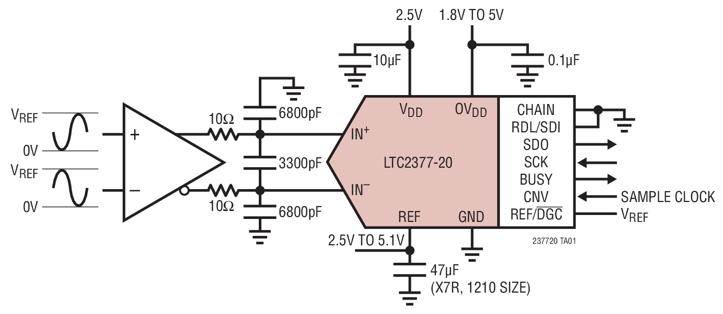
LTC2377-20 Demo Board | 20-Bit, 500ksps, SAR ADC with 104dB SNR. Requires DC2026
Analog Devices Inc.The LTC2378-20, LTC2377-20 and LTC2376-20 are 20‑bit, low power, low noise SAR ADCs with serial outputs that operate from a single 2.5V supply. The demo manual refers to the LTC2378-20 but applies to all parts in the family, the only difference being the maximum sample rate. The LTC2378-20 supports a ±5V fully differential input range with a 104dB SNR, consumes only 21mW and achieves ±2ppm INL max with no missing codes at 20 bits. The DC1925A demonstrates the DC and AC performance of the LTC2378-20 in conjunction with the DC590 QuikEval™ and DC890 PScope™ data collection boards. Use the DC590 to demonstrate DC performance such as peak-to-peak noise and DC linearity.

DC1930A
Analog Devices Inc.The LT3744 is a fixed frequency synchronous step-down DC/DC controller designed to drive a LED load at up to 20A continuous or 40A pulsed. The peak current mode controller will maintain ?3% LED current regulation over a wide output voltage range, from VEE to VIN. By allowing VEE to float to negative voltages, several LEDs in series can be driven from a single Li-Ion battery with a simple, single step-down output stage. PWM dimming is achieved with the PWM pins. The regulated LED current is set with analog voltages at the CTRL pins. Regulated voltage and overvoltage protection are set with a voltage divider from the output to the FB pin. The switching frequency is programmable from 100kHz to 1MHz through an external resistor on the RT pin.Additional features include an accurate external reference voltage, a control input for thermally derating regulation current, an accurate EN/UVLO pin, an open-drain output fault flag, OVLO, frequency synchronization, and thermal shutdown.Applications LED Driver for DLP Projectors Heads-Up Displays High Power LED

LT3072 Demo Board | Dual, Low Noise, 2.5A Programmable Output, Low Dropout Linear Regulator
Analog Devices Inc.Demonstration Circuit 1938A features the LT3072 dual, low noise, 2.5A programmable output, low dropout linear regulator. The input voltages VIN1 and VIN2 are independent and can range from 0.8V to 3.45V. Each channel has jumpers to set a three-bit code that determines output voltages VOUT1 and VOUT2 at pre-programmed levels with a range from 0.6V to 2.5V and a maximum output current of 2.5A. DC1938A requires a single external BIAS voltage that is higher than VIN1 and VIN2, between 2.375V and 5.25V and is at least 1.2V higher than the highest output voltage.
Each output is decoupled by a 1µF + 2.2µF + 6.8µF capacitor network and each input is decoupled with a 22µF capacitor. The internal reference of each channel is bypassed with a 0.1µF capacitor to reduce output noise and program the soft-start. 1500µF aluminum electrolytic capacitors and 220µF tantalum polymer capacitors hold up VIN1 and VIN2 but the aluminum electrolytic capacitors are cabling dependent and are not required on customer circuits. The BIAS voltage is bypassed at each channel’s BIAS pin with a 2.2µF capacitor and there is a single terminal for the BIAS input.
The positions of the VOUT1 and VOUT2 ENABLE jumpers either pull up the EN1 and EN2 pins to the BIAS voltage by a 100k resistor, short EN1 and EN2 to ground or float EN1 and EN2 so they can be driven directly by a signal applied to the EN1 and EN2 terminals. Each channel has a terminal for PWRGD that is pulled up to BIAS by a 51kΩ resistor. Resistors program a 3A output current limit and a 333mV/A output current monitoring voltage that is available at the IMON/LIM terminals. The TEMP terminal allows monitoring of die temperature.
VOIC allows automatic control of a pre-regulation voltage and the VOIC pins are bypassed with 1nF capacitors. MARGA1 and MARGA2 terminals for margining allow an
optional external voltage to program an adjustment to each channel’s output voltage.
Banana jacks minimize voltage drops on VIN and VOUT connections. Each channel’s SENSE pin terminates at a 10µF capacitor near the VOUT banana jacks. The PCB design minimizes parasitic SENSE to GND and SENSE to OUT trace capacitance. VO1+, VO1-, VO2+ and VO2- terminals Kelvin-connect to the 10µF VOUT capacitors and are the optimal place to observe output voltage regulation and load transient response. Each output has a 560Ω pre-load so the minimum load requirement is met over the VOUT programming range.
DC1938A has placeholders identified on the schematic as optional (Opt) components that make it convenient to add capacitance, add filtering, parallel references or use the VOIC function – check the schematic for placeholder locations.
The LT3072 is well suited to microprocessor systems and instrumentation applications with stringent performance requirements for output noise and load transient response. Systems with high efficiency requirements will benefit from the low dropout of the LT3072. DC1938A features the LT3072 in a thermally enhanced 36-lead 4mm × 7mm QFN package. The LT3072 data sheet must be read in conjunction with this demo manual to properly use or modify demo circuit DC1938A.

DC1941D
Analog Devices Inc.The LTC6820 provides bidirectional SPI communications between two isolated devices through a single twisted-pair connection. Each LTC6820 encodes logic states into signals that are transmitted across an isolation barrier to another LTC6820. The receiving LTC6820 decodes the transmission and drives the slave bus to the appropriate logic states. The isolation barrier can be bridged by a simple pulse transformer to achieve hundreds of volts of isolation.The LTC6820 drives differential signals using matched source and sink currents, eliminating the requirement for a transformer center tap and reducing EMI. Precision window comparators in the receiver detect the differential signals. The drive currents and the comparator thresholds are set by a simple external resistor divider, allowing the system to be optimized for required cable lengths and desired signal-to-noise performance.Applications Industrial Networking Battery Monitoring Systems Remote Sensors

LTC2185 and LTC6409 Combo Board with differential inputs, requires DC890, LVDS_XFMR and DC1075
Analog Devices Inc.DC1945A: Demo Board for the LTC2185 - 16-Bit, 125Msps Low Power Dual ADCs and LTC6409 - 10GHz GBW, 1.1nV/√Hz Differential Amplifier/ADC Driver.


