Evaluation Board for High-Speed Triple 2:1 Miltiplexer in the 16-Pin SSOP Package
Texas InstrumentsEvaluation Board for High-Speed Triple 2:1 Miltiplexer in the 16-Pin SSOP Package

TPS22968N-Q1 5.5V; 4A; 27mΩ; Dual-Channel Automotive Load Switch Evaluation Module
Texas InstrumentsTPS22968N-Q1 5.5V; 4A; 27mΩ; Dual-Channel Automotive Load Switch Evaluation Module

ADS5409 evaluation module for dual channels up to 900 MSPS
Texas InstrumentsADS5409 evaluation module for dual channels up to 900 MSPS

High Performance Frequency Synthesizer System with Integrated VCO (952 - 1137 MHz; 1904 - 2274 MHz)
Texas InstrumentsHigh Performance Frequency Synthesizer System with Integrated VCO (952 - 1137 MHz; 1904 - 2274 MHz)


8-A Active Bus Termination/DDR Memory DC/DC Converter
Texas Instruments8-A Active Bus Termination/DDR Memory DC/DC Converter


DAC3152 Dual-Channel; 10-Bit; 500-MSPS Digital-to-Analog Converter Evaluation Module
Texas InstrumentsDAC3152 Dual-Channel; 10-Bit; 500-MSPS Digital-to-Analog Converter Evaluation Module

Ultra Low Noise, 150mA Linear Regulator for RF Analog Circuits Requires No Bypass Capacitor
Texas InstrumentsUltra Low Noise, 150mA Linear Regulator for RF Analog Circuits Requires No Bypass Capacitor

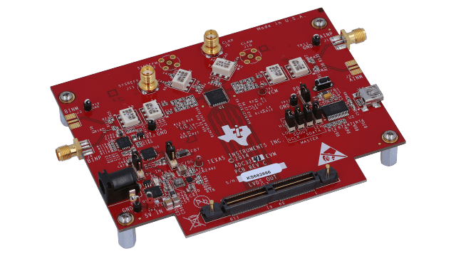
ADC3241 Dual-Channel; 14-Bit; 25-MSPS Analog-to-Digital Converter Evaluation Module
Texas InstrumentsADC3241 Dual-Channel; 14-Bit; 25-MSPS Analog-to-Digital Converter Evaluation Module


1-MHz; 3.3V; High-Efficiency Synchronous Buck Converter with TPS43000 PWM
Texas Instruments1-MHz; 3.3V; High-Efficiency Synchronous Buck Converter with TPS43000 PWM


TPS7A7200 Low-Dropout (LDO) Linear Regulator Evaluation Module
Texas InstrumentsTPS7A7200 Low-Dropout (LDO) Linear Regulator Evaluation Module

Evaluation module for TCA7408 and TCA5405
Texas InstrumentsEvaluation module for TCA7408 and TCA5405


