LTC2927 | Single Power Supply Tracking Controller
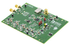
Analog Devices Inc.DC817A: Demo Board for the LTC2927 Single Power Supply Tracking Controller.
DC823B-A
Analog Devices Inc.The LTM4600 is a complete 10A, DC/DC step down power supply. Included in the package are the switching controller, power FETs, inductor, and all support components. Operating over an input voltage range of 4.5V to 20V, the LTM4600 supports an output voltage range of 0.6V to 5V, set by a single resistor. This high efficiency design delivers 10A continuous current (14A peak), needing no heat sinks or airflow to meet power specifications. Only bulk input and output capacitors are needed to finish the design.The low profile package (2.82mm) enables utilization of unused space on the bottom of PC boards for high density point of load regulation. High switching frequency and an adaptive on-time current mode architecture enables a very fast transient response to line and load changes without sacrificing stability. Fault protection features include integrated overvoltage and short circuit protection with a defeatable shutdown timer. A built-in soft-start timer is adjustable with a small capacitor.The LTM4600 is packaged in a compact (15mm ? 15mm) and low profile (2.82mm) over-molded Land Grid Array (LGA) package suitable for automated assembly by standard surface mount equipment. The LTM4600 is RoHS compliant.Applications Telecom and Networking Equipment Servers Industrial Equipment Point of Load Regulation
LT3028DHC Demo Board | Dual Input, Dual Output Linear Regulator, 2.3V ≤ VIN ≤ 20V, VOUT1 = 2.5V/3.3V/5V @ 500mA, VOUT2 = 2.5V/3.3V/5V @ 100mA
Analog Devices Inc.Demonstration circuit 832 is a dual output, dual input regulator consisting of two LDO linear regulators, based on the LT3028 monolithic linear regulator in the 5×3 DFN-16 package. Each independent input has a voltage range of 2.3V to 20V, with one output (VOUT1) capable of delivering up to 500mA of output current, and the other output (VOUT2) capable of delivering up to 100mA of output current. The two output voltages are set independently with jumpers; each can be set to 2.5V, 3.3V, 5V or a user-defined value (two jumper options for this).
The DC quiescent current is typically only 50uA (for the entire IC) at no load.
LTC3026EDD | Low VIN, VLDO Linear Regulator, 1.14V ≤ VIN ≤ 5.5V (3.5V Using Internal Boost), VOUT = 0.8V/1.2V/1.5V/1.8V/Adjustable @ 1.5A
Analog Devices Inc.Demonstration circuit 833 is an ultralow dropout voltage supply using the 1.5A output current LTC3026 linear regulator in a small 3mm × 3mm 10-Pin DFN package. The DC833 has an input voltage range from 1.14V to 3.5V when the internal boost converter is enabled, and a maximum input voltage of 5.5V when an external source is supplied. The output voltage jumper-selectable and can be set to 0.8V, 1.2V, 1.5V, 1.5V, 1.8V or a user-defined value between 0.4V and 2.6V. The 0.4V reference of the LTC3026 allows the DC833 to supply power to very low voltage applications. The DC833 is also an excellent choice for post regulation of step-down switching regulators, creating a high efficiency low-noise supply. The DC833 comes assembled with small ceramic capacitors, showing the LTC3026's ability to maintain stability with ceramic output capacitors.
DC841A
Analog Devices Inc.The LT3477 is a current mode, 3A DC/DC step-up converter with dual rail-to-rail current sense amplifiers and an internal 3A, 42V switch. It combines a traditional voltage feedback loop and two unique current feedback loops to operate as a constant-current, constant-voltage source. Both current sense voltages are set at 100mV and can be adjusted independently using the IADJ1 and IADJ2 pins. Efficiency of up to 93% can be achieved in typical applications. The LT3477 features a programmable soft-start function to limit inductor current during start-up. Both inputs of the error amplifier are available externally allowing positive and negative output voltages (boost, inverting, SEPIC, Flyback). The switching frequency is programmable from 200kHz to 3.5MHz through an external resistor.Available in thermally enhanced 20-pin (4mm ? 4mm) QFN and 20-pin TSSOP packages, the LT3477 provides a complete solution for both constant-voltage and constantcurrent applications.Applications High Power LED Driver DSL Modems Distributed Power Input/Output Current Limited Boost, SEPIC, Inverting, Flyback Converters Constant-Voltage, Constant-Current Source
DC843A
Analog Devices Inc.The LT3479 is a current mode, fixed frequency step-up DC/DC converter with an internal 3A, 42V switch. Efficiencies of up to 89% can be achieved in typical applications. It features a programmable soft-start function to limit inductor current during start-up and inrush current protection to protect the LT3479 during shorts and line transients. Both inputs of the error amplifier are available to the user allowing positive and negative output voltages. Through an external resistor, the user can program the switching frequency from 200kHz to 3.5MHz. The low profile (0.75mm) 14-pin, 4mm ? 3mm DFN package provides excellent thermal performance in a small footprint. The LT3479 is also available in a thermally enhanced 16-pin TSSOP package.Applications High Power LED Driver DSL Modems Distributed Power
LTC2446UHF | 24-Bit High Speed 4-/8-Channel Delta Sigma ADC (Requires DC590)
Analog Devices Inc.DC847A: Demo Board for the LTC2446 24-Bit High Speed 8-Channel Delta Sigma ADCs with Selectable Multiple Reference Inputs.
DC848A
Analog Devices Inc.The LTC4066/LTC4066-1 are USB power managers and Li-Ion battery chargers designed to work in portable battery-powered applications. The parts control the total current used by the USB peripheral for operation and battery charging. The total input current can be limited to 100mA, 500mA or ?unlimited? (i.e., above 2A). Battery charge current is automatically reduced such that the sum of the load current and the charge current does not exceed the programmed input current limit.The LTC4066/LTC4066-1 include a standalone constant-current / constant-voltage linear charger for single cell Li-ion batteries. The ?oat voltage applied to the battery is held to a tight 0.8% tolerance, and charge current is programmable using an external resistor to ground. A programmable end-of-charge status output (CHRG) indicates full charge. BAT pin charge and discharge currents can be monitored via an analog output (ISTAT). Total charge time is programmable by an external capacitor to ground. When the battery drops 100mV below the ?oat voltage, automatic recharging of the battery occurs. Also featured is an NTC thermistor input used to monitor battery temperature while charging.The LTC4066/LTC4066-1 are available in a 24-pin thin pro?le (0.75mm) 4mm x 4mm QFN package. The LTC4066 is also available in a 24-pin ultrathin pro?le (0.55mm) 4mm x 4mm UTQFN package.Applications Portable USB Devices GPS, Cameras, Broadband Wireless Modems Mulitple Input Chargers
LTC2298IUP | DeMUX Dual ADC, +3.0V, 65Msps 14-Bit 1MHz < AIN < 70MHz, (Requires DC890)
Analog Devices Inc.DC851A-B: Demo Board for the LTC2298 Dual 14-Bit, 65Msps Low Power 3V ADCs.
DC851A-D
Analog Devices Inc.The LTC2298/LTC2297/LTC2296 are 14-bit 65Msps/40Msps/25Msps, low power dual 3V A/D converters designed for digitizing high frequency, wide dynamic range signals. The LTC2298/LTC2297/LTC2296 are perfect for demanding imaging and communications applications with AC performance that includes 74.3dB SNR and 90dB SFDR for signals at the Nyquist frequency.DC specs include ?1.2LSB INL (typ), ?0.5LSB DNL (typ) and no missing codes over temperature. The transition noise is a low 1LSBRMS.A single 3V supply allows low power operation. A separate output supply allows the outputs to drive 0.5V to 3.6V logic. An optional multiplexer allows both channels to share a digital output bus.A single-ended CLK input controls converter operation. An optional clock duty cycle stabilizer allows high performance at full speed for a wide range of clock duty cycles.Applications Wireless and Wired Broadband Communication Imaging Systems Spectral Analysis Portable Instrumentation
LTC2293IUP | DeMUX Dual ADC, +3.0V, 65Msps 12-Bit 1MHz < AIN < 70MHz, (Requires DC890)
Analog Devices Inc.DC851A-I: Demo Board for the LTC2293 Dual 12-Bit, 65Msps Low Power 3V ADCs.
DC851A-O
Analog Devices Inc.The LTC2289 is a 10-bit 80Msps, low noise 3V dual A/D converter designed for digitizing high frequency, wide dynamic range signals. The LTC2289 is perfect for demanding imaging and communications applications with AC performance that includes 61.6dB SNR and 85dB SFDR for signals well beyond the Nyquist frequency.DC specs include ?0.1LSB INL (typ), ?0.1LSB DNL (typ) and ?0.6LSB INL, ?0.5LSB DNL over temperature. The transition noise is a low 0.08LSBRMS.A single 3V supply allows low power operation. A separate output supply allows the outputs to drive 0.5V to 3.6V logic. An optional multiplexer allows both channels to share a digital output bus.A single-ended CLK input controls converter operation. An optional clock duty cycle stabilizer allows high performance at full speed for a wide range of clock duty cycles.Applications Wireless and Wired Broadband Communication Imaging Systems Spectral Analysis Portable Instrumentation
LTC2286IUP | DeMUX Dual ADC, +3.0V, 25Msps 10-Bit 1MHz < AIN < 70MHz, (Requires DC890)
Analog Devices Inc.DC851A-R: Demo Board for the LTC2286 Dual 10-Bit, 25Msps Low Noise 3V ADCs.
DC854D-J
Analog Devices Inc.The LTC2216/LTC2215 are 80Msps/65Msps sampling 16- bit A/D converters designed for digitizing high frequency, wide dynamic range signals with input frequencies up to 400MHz. The input range of the ADC is ?xed at 2.75VP-P.The LTC2216/LTC2215 are perfect for demanding communications applications, with AC performance that includes 81.5dBFS noise ?oor and 100dB spurious free dynamic range (SFDR). Ultra low jitter of 85fsRMS allows undersampling of high input frequencies while maintaining excellent noise performance. Maximum DC specs include ?3.5LSB INL, ?1LSB DNL (no missing codes). The digital output can be either differential LVDS or single-ended CMOS. There are two format options for the CMOS outputs: a single bus running at the full data rate or demultiplexed buses running at half data rate. A separate output power supply allows the CMOS output swing to range from 0.5V to 3.6V. The ENC+ and ENC? inputs may be driven differentially or single-ended with a sine wave, PECL, LVDS, TTL or CMOS inputs. An optional clock duty cycle stabilizer allows high performance at full speed with a wide range of clock duty cycles.Applications Telecommunications Receivers Cellular Base Stations Spectrum Analysis Imaging Systems ATE
LT6555CGN | High Speed Triple 2:1 Video Multiplexer, VCC = 3.3V to 5V, VEE = –3.3V to –5V
Analog Devices Inc.DC858A: Demo Board for the LT6555 650MHz Gain of 2 Triple 2:1 Video Multiplexer.
LTC3221EDC-3.3 Demo Board | Micropower Regulated Charge Pump, 1.8V ≤ VIN ≤ 4.4V, VOUT = 3.3V @ Up to 60mA
Analog Devices Inc.Demonstration circuit 862 is a micropower regulated charge pump DC/DC converter featuring the 60mA output LTC3221 in a 2mmx2mm DFN package. It comes in three assembly versions, DC862A-A, DC862A-B and DC862A-C, featuring the LTC3221EDC-3.3 (fixed 3.3V output), the LTC3221EDC-5 (fixed 5V output) , and LTC3221EDC (adjustable output set to 3V), respectively. The demo board input voltage range depends on the IC used; for the 3.3V output DC862A-A, the input voltage range is 1.8V to 4.4V.
The LTC3221's low 8µA no-load quiescent current is even lower than the self-discharging current of many batteries. By employing a constant current to charge the output, the output ripple is low even at high input and light load, and is fairly constant over the full input voltage range.
DC866A
Analog Devices Inc.The LT6550/LT6551 are 3.3V triple and quad high speed video amplifiers. These voltage feedback amplifiers drive double terminated 50? or 75? cables and are configured for a fixed gain of 2, eliminating six or eight external gain setting resistors. The LT6550/LT6551 feature 110MHz ?3dB bandwidth, high slew rates and fast settling, making them ideal for RGB video processing.The LT6551 quad is designed for single supply operation and the LT6550 triple can be used on either single or split supplies. On a single 3.3V supply, the input voltage range extends from ground to 1.55V and the output swings to within 400mV of the supply voltage while driving a 150? load. These features, combined with the ability to accept RGB video signals without the need for AC coupling or level shifting of the incoming signals, make the LT6550/LT6551 an ideal choice for low voltage video applications.Both the LT6550 and LT6551 are available in the small 10-Pin MSOP package and utilize a flow-thru pin out. The small footprint results in a compact high performance video amplifier solution.Applications Automotive Displays LCD and CRT Compatible RGB Amplifiers Coaxial Cable Drivers Low Voltage High Speed Signal Processing Set Top Boxes
LTC3827EG-1 Demo Board
Analog Devices Inc.DC868A: Demo Board for the LTC3827-1 Low IQ, Dual, 2-Phase Synchronous Step-Down Controller.
LTC3215EDD | Low Noise, High Current LED Flash Charge Pump, VIN = 2.9V to 4.4V, AOT
Analog Devices Inc.DC871A-A: Demo Board for the LTC3215 700mA Low Noise High Current LED Charge Pump.
LTC1867LCGN Demo Board | 3V, 16-Bit, 8-Channel (Requires DC2026)
Analog Devices Inc.Demonstration circuit 873 features the LTC1867L Octal 16-bit ADC. The LTC1867L can be software programmed for a unipolar 0 to 2.5V or bipolar ±1.25V input range. The 8 channel multiplexer can be programmed for 8 single-ended inputs with respect to ground, 7 single-ended inputs with respect to the COM/CH7 pin, 4 differential inputs, or any combination of these.


