
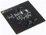


Evaluation Module for TPS24701 Positive Voltage Power-Limiting Hotswap Controller
Texas InstrumentsEvaluation Module for TPS24701 Positive Voltage Power-Limiting Hotswap Controller

Evaluation Module for BQ24600 Multi Cell Synchronous Switch-Mode Charger
Texas InstrumentsEvaluation Module for BQ24600 Multi Cell Synchronous Switch-Mode Charger
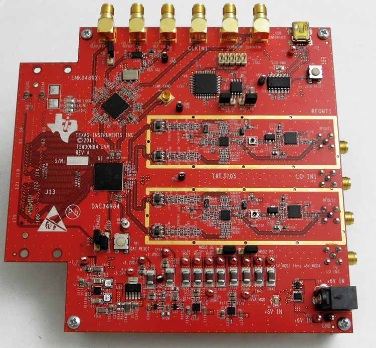
Wideband Transmit Signal Chain Evaluation Board and Reference Design
Texas InstrumentsWideband Transmit Signal Chain Evaluation Board and Reference Design
3.3/5Vin, 9-A Sequencing DC/DC Converter Module
Texas Instruments3.3/5Vin, 9-A Sequencing DC/DC Converter Module


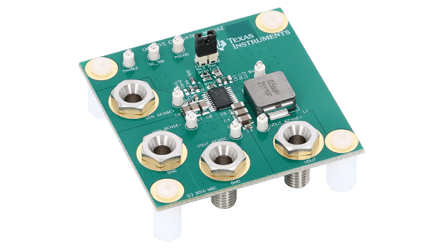
3A 550 kHz Synchronous SIMPLE SWITCHER? Buck Regulator Evaluation Module
Texas Instruments3A 550 kHz Synchronous SIMPLE SWITCHER? Buck Regulator Evaluation Module
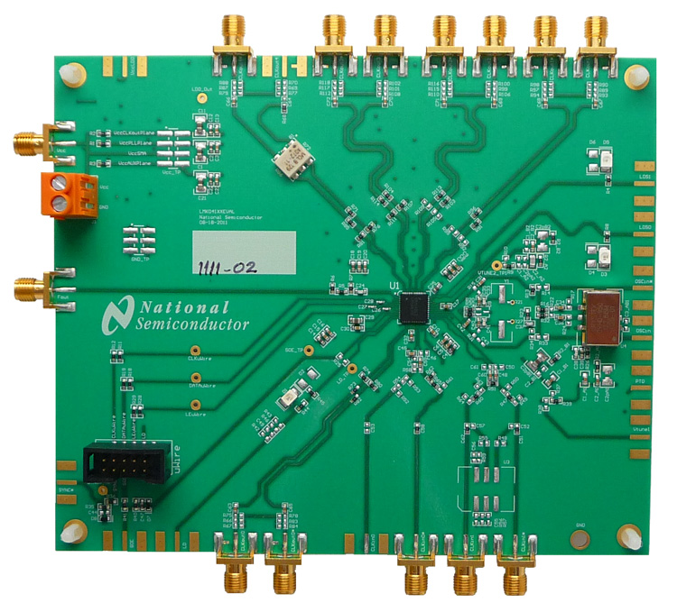
LMK04100 Clock Jitter Cleaner with Cascade PLL
Texas InstrumentsLMK04100 Clock Jitter Cleaner with Cascade PLL
BQ24314 Evaluation Module
Texas InstrumentsThe bq2431x evaluation module is a complete charger module for evaluating a charger front-end protection and charger solution using the bq2431x and bq24080 devices. It is designed to deliver up to 700 mA of charge current to Li-ion or Li-polymer applications. The charger front-end protection current is designed to 1000 mA. The bq2431x protects the charging system against three types of failures: input overvoltage when the AC adapter fails to regulate its voltage; load overcurrent when failures such as a short circuit occur in the charging system; and battery overcharge.
Features:
Evaluation module for bq2431x DSJ
Evaluation module for bq24080 charger IC
Evaluation module for bq2431x and bq24080 chipset solution
Input operating range for bq2431x 4.5 V–26 V
Input operating range for bq24080 4.5 V–6.5 V
Input overvoltage protection
Input overcurrent protection
Battery overvoltage protection
LED indication for status signals
Test points for key signals available for testing purpose. Easy probe hook-up
Jumpers available. Easy to change connections


