Manufacturer
MORE
Stock

Displaying 1101 - 1120 of 11824

Evaluation Kits

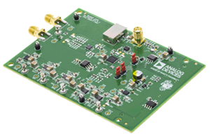
EVAL-ADATE324EBZ

Analog Devices Inc.
The ADATE324 is a complete, single-chip, quad-channel automatic test equipment (ATE) solution that performs the pin electronics (PE) functions of a driver, a comparator, and an active load (DCL). The device also features a high voltage (VHH) drive capability per chip to support flash memory testing applications. Dedicated 16-bit digital-to-analog converters (DACs) with on-chip calibration registers provide all the necessary dc levels for operation of the device.The voltage driver features three active states: high, low, and terminate mode, as well as a high impedance inhibit state. The inhibit state, in conjunction with the integrated dynamic clamps, facilitates significant attenuation of transmission line reflections when the driver is not actively terminating the line. The open circuit drive capability is ?1.5 V to +4.5 V to accommodate the standard range of ATE and instrumentation applications.The ADATE324 can be used as a quad, single-ended, pin electronics channel or as a dual differential channel. In additional to per channel, high speed window comparators, the ADATE324 provides two programmable threshold differential comparators for differential ATE applications.All dc levels for DCL functions are generated by dedicated on-chip 16-bit DACs. To facilitate accurate programming levels, the ADATE324 also includes an integrated calibration function to correct for gain and offset errors of each functional block. Correction coefficients can be stored on chip, and any values written to the DACs are automatically adjusted using the appropriate correction factors.The ADATE324 uses a serial programmable interface (SPI) bus to program all functional blocks, DACs, and on-chip calibration constants. The device also has an on-chip temperature sensor, and overvoltage and undervoltage fault clamps, for monitoring and reporting the device temperature, and any output pin voltage faults that may occur during operation.For more information on the ADATE324, contact ADATE324@analog.com.APPLICATIONS ATE Semiconductor and board test systems Instrumentation and characterization equipment

EVAL-ADBMS1818Z

Analog Devices Inc.
The ADBMS18181 is a multicell battery stack monitor that measures up to 18 series connected battery cells with a total measurement error of less than 3.0 mV. The cell measurement range of 0 V to 5 V makes the ADBMS1818 suitable for most battery chemistries. All 18 cells can be measured in 290 ?s, and lower data acquisition rates can be selected for high noise reduction. Multiple ADBMS1818 devices can be connected in series, permitting simultaneous cell monitoring of long, high voltage battery strings. Each ADBMS1818 has an isoSPI? interface for high speed, RF immune, long distance communications. Multiple devices are connected in a daisy chain with one host processor connection for all devices. This daisy chain can be operated bidirectionally, ensuring communication integrity, even in the event of a fault along the communication path. The ADBMS1818 can be powered directly from the battery stack or from an isolated supply. The ADBMS1818 includes passive balancing for each cell, with individual PWM duty cycle control for each cell. Other features include an on-board 5 V regulator, nine general purpose I/O lines, and a sleep mode, where current consumption is reduced to 6 ?A. All registered trademarks and trademarks are the property of their respective owners. 1 Protected by multiple U.S. patents, including 8908779, 9182428, and 9270133. APPLICATIONS Backup battery systems Grid energy storage Residential energy storage UPS High power portable equipment

EVAL-ADBMS6816

Analog Devices Inc.
The ADBMS6816 is a multicell battery stack monitor that measures up to six series connected battery cells with a lifetime total measurement error (TME) of less than 1.5 mV. The cell measurement range of 0 V to 5 V makes the ADBMS6816 suitable for most battery chemistries. All six cells can be measured in 304 ?s, and lower data acquisition rates can be selected for high noise reduction.Multiple ADBMS6816 devices can be connected in series, permitting simultaneous cell monitoring of long, high voltage battery strings. Each ADBMS6816 has an isoSPI? interface for high speed, RF immune, long distance communications.Multiple devices are connected in a daisy chain with one host processor connection for all devices. This daisy chain can be operated bidirectionally, ensuring communication integrity even in the event of a fault along the communication path.The ADBMS6816 can be powered directly from the battery stack or from an isolated supply. The ADBMS6816 includes passive balancing for each cell, with individual pulse-width modulation (PWM) duty cycle control for each cell. Other features include an on-board 5 V regulator, seven general-purpose input/output (GPIO) lines, and a sleep state, where current consumption is reduced to 5.5 ?A.APPLICATIONS Electric and hybrid electric vehicles Backup battery systems Grid energy storage High power portable equipment

EVAL-ADCMP564BRQZ

Analog Devices Inc.
The ADCMP563/ADCMP564 are high speed comparatorsfabricated on Analog Devices? proprietary XFCB process. Thedevices feature a 700 ps propagation delay with less than 75 psoverdrive dispersion. Dispersion, a measure of the difference inpropagation delay under differing overdrive conditions, is a particularlyimportant characteristic of high speed comparators. A separateprogrammable hysteresis pin is available on the ADCMP564.A differential input stage permits consistent propagation delaywith a wide variety of signals in the common-mode range from?2.0 V to +3.0 V. Outputs are complementary digital signals thatare fully compatible with ECL 10 K and 10 KH logic families.The outputs provide sufficient drive current to directly drivetransmission lines terminated in 50 ? to ?2 V. A latch input,which is included, permits tracking, track-and-hold, or sample-and-holdmodes of operation. The latch input pins contain internalpull-ups that set the latch in tracking mode when left open.The ADCMP563/ADCMP564 are specified over the industrialtemperature range (?40?C to +85?C).Applications Automatic test equipment High speed instrumentation Scope and logic analyzer front ends Window comparators High speed line receivers Threshold detection Peak detection High speed triggers Patient diagnostics Hand-held test instruments Zero crossing detectors Line receivers and signal restoration Clock drivers

EVAL-ADCMP604BKSZ

Analog Devices Inc.
The ADCMP604 / ADCMP605?are very fast comparators fabricated on the Analog Devices, Inc. proprietary XFCB2 process. These comparators are exceptionally versatile and easy to use. Features include an input range from VEE ? 0.5 V to VCCI + 0.2 V, low noise, LVDS-compatible output drivers, and TTL/CMOS latch inputs with adjustable hysteresis and/or shut-down inputs.The devices offer 1.5 ns propagation delays with 1 ps rms random jitter (RJ). Overdrive and slew rate dispersion are typically less than 50 ps.A flexible power supply scheme allows the devices to operate with a single 2.5 V positive supply and a ?0.5 V to +2.7 V input signal range up to a 5.5 V positive supply with a ?0.5 V to +5.7 V input signal range. Split input/output supplies, with no sequencing restrictions on the ADCMP605, support a wide input signal range with greatly reduced power consumption.The LVDS-compatible output stage is designed to drive any standard LVDS input. The comparator input stage offers robust protection against large input overdrive, and the outputs do not phase reverse when the valid input signal range is exceeded. High speed latch and programmable hysteresis features are also provided in a unique single-pin control option.The ADCMP604 is available in a 6-lead SC70 package, and the ADCMP605 is available in a 12-lead LFCSP.APPLICATIONS High speed instrumentation Clock and data signal restoration Logic level shifting or translation Pulse spectroscopy High speed line receivers Threshold detection Peak and zero-crossing detectors High speed trigger circuitry Pulse-width modulators Current-/voltage-controlled oscillators Automatic test equipment (ATE)

EVAL-ADE1201EBZ

Analog Devices Inc.
The ADE12011 is a single channel, configurable, isolated?digital input monitoring solution for energy transmission and?distribution applications. The ADE1201 is configured through?the serial port interface (SPI) to perform an isolated measurement?of the digital input that is also called binary input or contact?input. The ADE1201 digital output signal on the DOUT1 pin?reflects the state of the input signal after user configurable?signal conditioning. The SPI protocol supports addressing to?allow up to eight devices sharing one 4-wire SPI port.The ADE1201 application circuit accepts a wide range of input?voltages from ?10 V dc to ?300 V dc, or 8 V rms to 240 V rms.?The programmable wetting current and robust application?circuit enable the device to meet stringent, system level?electromagnetic capability (EMC) requirements.The ADE1201 includes an isoPower? integrated, isolated dc-to-dc?converter that eliminates the need for an external isolated power?supply. The iCoupler? chip scale transformer technology is?used to isolate the logic signals between the high voltage,?isolated side and the low voltage, nonisolated side of the?digital input monitor. This technology creates a small form?factor design that includes data and power isolation.An integrated successive approximation register (SAR)?analog-to-digital converter (ADC) and a programmable gain?amplifier (PGA) from 1? to 10? measure the analog inputs.?The ADC waveforms are available through the SPI port to?allow system level diagnostics.Product Highlights Single channel, configurable, isolated digital input. Single hardware design supports 24 V to 300 V systems. Robust architecture. Enables system level diagnostics.Applications Energy transmission and distribution Multifunction relay protection Substation battery monitoring Bay or substation interlocking Merge unit Circuit breaker status indication Remote terminal unit Building automation1 Protected by U.S. Patent Number 2017/0250043. Other patents pending.

EVAL-ADF7021-VDB1Z

Analog Devices Inc.
The ADF7021-V is a high performance, low power, narrow-band RF transceiver based on the ADF7021-N. The architecture of the ADF7021-V transceiver is similar to that of the ADF7021-N except that an external VCO is used by the on-chip RF synthesizer for applications that require improved phase noise performance.The ADF7021-V is designed to operate in both the license-free ISM bands and in the licensed bands from 80 MHz to 960 MHz.To minimize RF feedthrough and spurious emissions, the external VCO operates at 2? or 4? the desired RF frequency; the ADF7021-V supports a maximum VCO frequency operation of 1920 MHz. The 4? VCO operation is programmable by enabling an additional on-chip divide-by-2 outside the RF synthesizer loop and offers improved phase noise performance.As with the ADF7021-N receiver, the IF filter bandwidths of 9 kHz, 13.5 kHz, and 18.5 kHz are supported, making the ADF7021-V ideally suited to worldwide narrow-band telemetry applications.The part has both Gaussian and raised cosine transmit data filtering options to improve spectral efficiency for narrow-band applications. It is suitable for circuit applications targeted at the following: European ETSI EN 300 220 North American FCC Part 15, Part 90, and Part 95 Japanese ARIB STD-T67 Korean short-range device regulations Chinese short-range device regulationsA complete transceiver can be built using a small number of discrete external components, making the ADF7021-V very suitable for area-sensitive, high performance driven applications.See data sheet for more information.APPLICATIONS Narrow-band, short range device (SRD) standards ETSI EN 300 220 FCC Part 90 (meets Emission Mask D requirements) FCC Part 95 ARIB STD-T67 Wireless Metering Narrow-band wireless telemetry

EVAL-ADF7024DB1Z

Analog Devices Inc.
The ADF7024 is an ultralow power, integrated transceiver for use in the license-free ISM bands at 433 MHz, 868 MHz, and 915 MHz. Its ease of use and high performance make it suitable for a wide variety of wireless applications. The ADF7024 is suitable for operation under the European ETSI EN 300-220 regulation, the North American FCC Part 15 regulation, and other similar regulatory standards.The ADF7024 can operate under a number of predefined radio profiles. For each radio profile, optimized register settings are provided for the ADF7024 radio. This ensures that the RF communication layer works seamlessly, allowing the user to concentrate on the protocol and system level design and prototyping. The radio profiles cover common data rate and modulation options. There are six radio profiles in total, as shown in Table 1.The ADF7024 operates with a power supply range of 2.2 V to 3.6 V and has very low power consumption in both Tx and Rx modes, enabling long lifetimes in battery-operated systems while maintaining excellent RF performance.The low IF receiver minimizes power consumption and provides excellent sensitivity. The receiver is exceptionally linear and, therefore, is very resilient to the presence of interferers in spectrally noisy environments. The highly efficient transmitter has programmable output power up to 13.5 dBm and automatic power amplifier (PA) ramping to meet transient spurious specifications. The RF synthesizer comprises a voltage controlled oscillator (VCO), a low noise fractional-N phase-locked loop (PLL) and a loop filter, all of which are fully integrated and automatically calibrated. This agile frequency synthesizer facilitates the implementation of frequency-hopping spread spectrum (FHSS) systems.The smart wake mode (SWM) allows the ADF7024 to wake up autonomously from sleep using the internal wake-up timer without intervention from the host processor. This functionality allows carrier sense, packet sniffing, and packet reception while the host processor is in sleep, thereby reducing overall system current consumption.The ADF7024 eases the processing burden of the host processor by integrating the lower layers of a typical communication protocol stack. The host processor can configure the ADF7024 using a simple command-based protocol over a standard 4-wire SPI interface. A single-byte command transitions the radio between states or performs a radio function.A complete wireless solution can be built using a small number of external discrete components and a host processor (typically a microcontroller).For more information, see the ADF7024 Hardware Reference Manual, UG-698, which is only available as part of the ADF7024 design resource package.APPLICATIONS Wireless sensor networks (WSNs) Home and building automation Asset tracking Process and building control Industrial control Internet of Things (IoT)

EVAL_PAN4561

Panasonic Industrial Devices
RF Development Tools Eval kit PAN4561- (Synapse)

CYBT-343026-EVAL

Infineon Technologies AG
Bluetooth Development Tools - 802.15.1 CYBT-343026-EVAL

CYBLE-214015-EVAL

Infineon Technologies AG
Bluetooth Development Tools - 802.15.1 Module Kit

CYBLE-224116-EVAL

Infineon Technologies AG
Bluetooth Development Tools - 802.15.1 Module Kit

EVM3690-30B-BF-00A

Monolithic Power Systems (MPS)
Monolithic Power Systems (MPS) 16V, 36A, High-Efficiency, Synchronous Step-Down Module Evaluation Board

EVQ5073-G-00A

Monolithic Power Systems (MPS)
Power Management IC Development Tools MPQ5073 Evaluation Board

EVAL_PAN4561

Panasonic Industrial Devices
RF Development Tools Eval kit PAN4561- (Synapse)

KSZ8863RLL-EVAL

Microchip Technology Inc.
Ethernet Development Tools 3-Port Copper 10/100 Ethernet Switch with 1x RMII Interface - Evaluation Board

BMD-380-EVAL

u-blox
Bluetooth Development Tools - 802.15.1 EVK for BMD-380 with open CPUStand-alone Bluetooth Low EnergyInternal antenna

BMD-360-EVAL

u-blox
Bluetooth Development Tools - 802.15.1 EVAL BOARD FOR BMD-360 nRF52811

BMD-341-EVAL

u-blox
Bluetooth Development Tools - 802.15.1 EVAL BOARD FOR BMD-341 NRF52840

EVK-F9P-00

u-blox
u-blox EVK-F9P-00 Evaluation Kit The u-blox EVK-F9P-00 Evaluation Kits stand out as robust and multifunctional tools tailored for assessing the capabilities of high-precision positioning solutions. These kits come equipped with a built-in USB interface, offering both power supply and high-speed data transfer capabilities, thereby eliminating the necessity for an external power source. Their compact form factor, combined with an intuitive user interface, renders these evaluation kits exceptionally suitable for a broad spectrum of applications, spanning laboratory settings, vehicular contexts, and outdoor environments. Furthermore, the versatility of these devices extends to compatibility with notebook PCs, rendering them indispensable throughout the entirety of the design process. FEATURES Simplifies the evaluation of u-blox F9 high-precision positioning products Built-in USB interface (Type-C connector) for power supply and high-speed data transfer Eliminates the need for an external power supply 14-pin front connector to access all interfaces Successor kit to the C099-F9P application board  APPLICATIONS Laboratories Vehicles Outdoor locations Design-in process Evaluation of u-blox F9 high-precision positioning products  KIT CONTENTS  Compact 105mm x 64mm x 26mm EVK-F9P evaluation unit USB-A to USB-C cable 14-pin front connector breakout cable ANN-MB multi-band (L1/L2) active GNSS antenna with 5m cable Antenna ground plane EVK welcome card HxGN SmartNet promotional one-month service card 

Displaying 1101 - 1120 of 11824

Latest Parts

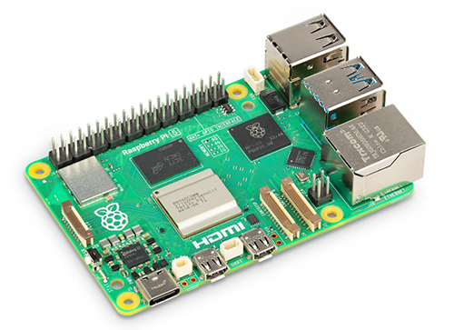
SC1112

Raspberry Pi

$79.61 - $86.40

IN STOCK 10239
Buy

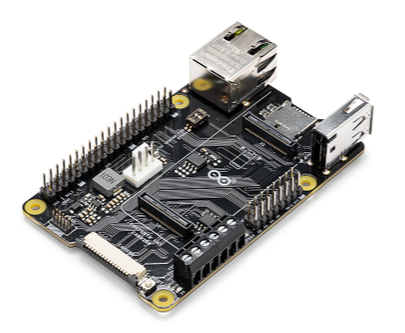
ASX00049

Arduino

* $39.28 - * $44.37

IN STOCK 3132
Buy

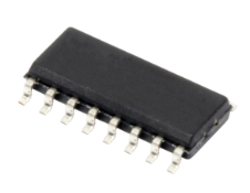
AD96685BRZ

Analog Devices Inc.

$1.72 - * $11.78

IN STOCK 4921
Buy

Reference Designs

RD006

Wurth Elektronik

RD006 - 3 W Dual-output isolated auxiliary supply for communication interfaces and measurement systems

CN0583

Analog Devices Inc.

Multistandard Micropower Verified Smoke Detection System-on-Module

Technical Resources

EVALUATION KITS

EVAL-AD7124-8SDZ

Analog Devices Inc.

$71.02 - * $75.91

IN STOCK 808
Buy
View All