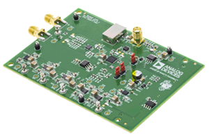
EV-ADF5610SD1Z
Analog Devices Inc.The ADF5610 allows implementation of fractional-N or Integer N phase-locked loop (PLL) frequency synthesizers when used with an external loop filter and an external reference source. The wideband microwave voltage controlled oscillator (VCO) design permits frequency operation from 7300 MHz to 14600 MHz at a single radio frequency (RF) output. A series of frequency dividers with a differential frequency output allows operation from 57 MHz to 14600 MHz. Analog and digital power supplies for the PLL circuitry range from 3.1 V to 3.5 V, and the VCO supplies are between 4.75 V and 5.25 V. The charge pump supply voltage can be extended up to 3.6 V for improved frequency band overlap and extended upper frequency range.The ADF5610 has an integrated VCO with a fundamental frequency of 3650 MHz to 7300 MHz. These frequencies are internally doubled and routed to the RFOUT pin. An additional differential output allows the doubled VCO frequency to be divided by 1, 2, 4, 8, 16, 32, 64, or 128, allowing the user to generate RF output frequencies as low as 57 MHz. A simple 3?wire serial port interface (SPI) provides control of all on-chip registers. To conserve power, this divider block can be disabled when not needed through the SPI interface. Likewise, the output power for both the single-ended output and the differential output are programmable via the VCO register settings. The ADF5610 also contains various power-down modes for the VCO circuitry and PLL circuitry.The integrated phase detector (PD) and delta-sigma (?-?) modulator, capable of operating at up to 100 MHz, permit wide loop bandwidths and fast frequency tuning with a typical spurious level of ?100 dBc.With phase noise levels from ?115 dBc/Hz at 7.3 GHz to ?109 dBc/Hz at 14.6 GHz, the ADF5610 is equipped to minimize blocker effects, and to improve receiver sensitivity and transmitter spectral purity. The low phase noise floor eliminates any contribution to modulator and mixer noise floor in transmitter applications.The ADF5610 is a PLL with integrated VCO. The device features an innovative programmable performance technology that enables the ADF5610 to tailor current consumption and corresponding noise performance to individual applications by selecting either a low current consumption mode or a high performance mode for improved phase noise performance.Additional features of the ADF5610 include approximately 3 dBof RFOUT gain control in 1.5 dB steps and 5 dB of control onthe differential port in approximately 2.5 dB steps. Finally, the ?-?modulator with exact frequency mode enables users to generateoutput frequencies with 0 Hz frequency error.APPLICATIONSMilitary and defenseTest equipmentClock generationWireless infrastructureSatellite and very small aperture terminal (VSAT)Microwave radio
EV-ADF5902SD1Z
Analog Devices Inc.The ADF5902 is a 24 GHz transmitter (Tx) monolithic microwaveintegrated circuit (MMIC) with an on-chip, 24 GHz voltagecontrolled oscillator (VCO). The VCO features a fractional-Nfrequency synthesizer with waveform generation capability withprogrammable grid array (PGA) and dual transmitter channelsfor radar systems. The on-chip, 24 GHz VCO generates the24 GHz signal for the two transmitter channels and the localoscillator (LO) output. Each transmitter channel contains apower control circuit. There is also an on-chip temperaturesensor.Control of all the on-chip registers is through a simple, 4-wireserial peripheral interface (SPI).The ADF5902 comes in a compact, 32-lead, 5 mm ? 5 mmLFCSP package. Applications Automotive radars Industrial radars Microwave radar sensors
EV-ADF70301-433AZ
Analog Devices Inc.The ADF7030-1 is a fully integrated, radio transceiver achieving high performance at very low power. The ADF7030-1 is ideally suited for applications that require long range, network robustness, and long battery life. It is suitable for applications that operate in the ISM, SRD, and licensed frequency bands at 169.4 MHz to 169.6 MHz, 426 MHz to 470 MHz, and 863 MHz to 960 MHz. It provides extensive support for standards-based protocols like IEEE802.15.4g while also providing flexibility to support a wide range of proprietary protocols.The highly configurable low intermediate frequency (IF) receiver supports a large range of receiver channel bandwidths from 2.6 kHz to 406 kHz. This range of receiver channel bandwidths allows the ADF7030-1 to support ultranarrow-band, narrow-band, and wideband channel spacing.The ADF7030-1 features two independent PAs supporting output power ranges of ?20 dBm to +13 dBm and ?20 dBm to +17 dBm. The PAs support ultrafine adjustment of the power with a step resolution of 0.1 dB. The PA output power is exceptionally robust over temperature and voltage. The PAs have an automatic power ramp control to limit spectral splatter to meet regulatory standards.The ADF7030-1 features an on-chip ARM??Cortex?-M0 processor that performs radio control, radio calibration, and packet management. Cortex-M0 eases the processing burden of the host processor because the ADF7030-1 integrates the lower layers of a typical communication protocol stack. This internal processor also permits the download and execution of Analog Devices, Inc., provided firmware modules that can extend the functionality of the ADF7030-1.The ADF7030-1 has two packet modes: generic packet mode and IEEE802.15.4g mode. In generic packet mode, the packet format is highly flexible and fully programmable, thereby ensuring its compatibility with proprietary packet formats. In IEEE802.15.4g packet mode, the packet format conforms to the?IEEE802.15.4g standard. FEC, as per the IEEE802.15.4g standard, is also supported.The ADF7030-1 operates with a power supply range of 2.2 V to 3.6 V and has very low power consumption in both Tx and Rx modes, enabling long lifetimes in battery-operated systems. An ultralow power deep sleep mode achieves a typical current of 10 nA with the configuration memory retained.A complete wireless solution can be built using a small number of external discrete components and a host processor (typically a microcontroller). The host processor can configure the ADF7030-1 using a simple command-based protocol over a standard 4-wire SPI interface. A single-byte command transitions the radio between states or performs a radio function.The ADF7030-1 is available in two package types: a 6 mm ? 6 mm, 40-lead LFCSP and a 7 mm ? 7 mm, 48-lead LQFP. Both package types use NiPdAu plating to mitigate against silver migration in high humidity applications. The ADF7030-1 operating temperature range is ?40?C to +85?C.For Figure 13 to Figure 19, Figure 30, Figure 42, Figure 60, Figure 61, and Figure 75 in the Typical Performance Characteristics section, PA_COARSE is a programmable value that provides a coarse adjustment of the PA output power. This value can be programmed in the range of 1 to 6 for PA1, and from 1 to 10 for PA2. PA_FINE is a programmable value that provides a fine adjustment of the PA output power. This value can be programmed in the range of 3 to 127 for both PA1 and PA2. PA_MICRO is a programmable value that provides a microadjustment (typically
EV-ADUCM322IQSPZ
Analog Devices Inc.The ADuCM322 is a fully integrated, single package device that incorporates high performance analog peripherals together with digital peripherals controlled by an 80 MHz ARM? Cortex?-M3 processor and integral flash for code and data.The ADC on the ADuCM322 provides 12-bit, 1 MSPS data acquisition on up to 16 input balls. Additionally, chip temperature and supply voltages can be measured.The ADC input voltage range is 0 V to VREF. A sequencer is provided, which allows a user to select a set of ADC channels to measure in sequence without software involvement during the sequence. The sequence can optionally repeat automatically at a user selectable rate. Up to eight VDACs are provided with output ranges that are programmable to one of two voltage ranges.The ADuCM322 can be configured so that the digital and analog outputs retain their output voltages through a watchdog or software reset sequence. Thus, a product can remain functional even while the ADuCM322 is resetting itself.The ADuCM322 has a low power ARM Cortex-M3 processor and a 32-bit RISC machine that offers up to 100 MIPS peak performance. Also integrated on-chip are 2 ? 128 kB Flash/EE memory blocks and 32 kB of SRAM. The flash comprises two separate 128 kB blocks supporting execution from one flash block and simultaneous writing/erasing of the other flash block.The ADuCM322 operates from an on-chip oscillator or a 16 MHz external crystal and a PLL at 80 MHz. This clock can optionally be divided down to reduce current consumption. Additional low power modes can be set via software. In normal operating mode, the ADuCM322 digital core consumes about 300 ?A per MHz.The device includes an MDIO interface capable of operating at up to 4 MHz. The capability to simultaneously execute from one flash block and write/erase the other flash block makes the ADuCM322 ideal for 10G, 40G, and 100G optical applications. In addition, the nonerasable kernel code plus flags in user flash provide assistance by allowing user code to robustly switch between the two blocks of user flash code and data spaces.The ADuCM322 integrates a range of on-chip peripherals that can be configured under software control, as required in the application. These peripherals include 1 ? UART, 2 ? I2C, and 2 ? SPI serial input/output communication controllers, GPIO, 32-element PLA, three general-purpose timers, plus a wake-up timer and system watchdog timer. A 16-bit PWM with seven output channels is also provided.GPIO balls on the device power up in high impedance input mode. In output mode, the software chooses between open-drain mode and push-pull mode. The pull-up resistors can be disabled and enabled in software. In GPIO output mode, the inputs can remain enabled to monitor the balls. The GPIO balls can also be programmed to handle digital or analog peripheral signals; in such cases, the ball characteristics are matched to the specific requirement.A large support ecosystem is available for the ARM Cortex-M3 processor to ease product development of the ADuCM322. Access is via the ARM serial wire debug port (SW-DP). On-chip factory firmware supports in-circuit serial download via MDIO. These features are incorporated into a QuickStart? development system, supporting this precision analog microcontroller family.APPLICATIONS Optical networking
EV-ADUCRF101QS1Z
Analog Devices Inc.The ADuCRF101 is a fully integrated, data acquisition solution that is designed for low power, wireless applications. It features a 12-bit analog-to-digital converter (ADC), a low power ARM Cortex?-M3 processor, a 862 MHz to 928 MHz and 431 MHz to 464 MHz RF transceiver, and Flash?/EE memory. The ADuCRF101 is packaged in a 9 mm ? 9 mm LFCSP.The data acquisition section consists of a 12-bit SAR ADC. The six inputs can be configured in single-ended or differential mode. When configured in single-ended mode, they can be used for ratiometric measurements on sensors that are powered, when required, from the internal low dropout regulator (LDO). An internal battery monitor channel and an on-chip temperature sensor are also available.This wireless data acquisition system is designed to operate in battery-powered applications where low power is critical. The device can be configured in normal operating mode or different low power modes under direct program control. In flexi mode, any peripheral can wake up the device and operate it. In hibernate mode, the internal wake-up timer remains active. In shutdown mode, only an external interrupt can wake up the device.The ADuCRF101 integrates a low power ARM Cortex-M3 processor. It is a 32-bit RISC machine, offering up to 1.25 DMIPS peak performance. The ARM Cortex-M3 processor also has a flexible 14-channel direct memory access (DMA) controller that supports communication peripherals, serial peripheral interface (SPI), UART, and I2C. Also provided on chip are 128 kB of nonvolatile Flash/EE memory and 16 kB of SRAM.A 16 MHz on-chip oscillator generates the system clock. This clock can be internally divided for the processor to operate at a lower frequency, thus saving power. A low power, internal 32 kHz oscillator is available and can be used to clock the four timers, as follows: two general-purpose timers, a wake-up timer, and a system watchdog timer.A range of communication peripherals can be configured, as required, in a specific application. These peripherals include UART, I2C, SPI, GPIO ports, PWM, and RF transceivers.The RF transceiver communicates in the 862 MHz to 928 MHz and 431 MHz to 464 MHz frequency bands using multiple configurations.On-chip factory firmware supports in-circuit serial download via the UART, and nonintrusive emulation and program download are also supported via the serial wire interface. These features are incorporated into a low cost development system supporting this precision analog microcontroller family.The ADuCRF101 operates from 2.2 V to 3.6 V and is specified over an industrial temperature range of ?40?C to +85?C. It is available in a 64-lead LFCSP packageApplications Battery powered wireless sensor Medical telemetry systems Industrial and home automation Asset tracking Security systems (access systems) Health and fitness applications??
EV-ADUM7703-8FMCZ
Analog Devices Inc.The ADuM7703 is a high performance, second-order, ?-? analog-to-digital converter (ADC) with an integrated low dropout (LDO) regulator that converts an analog input signal into a high speed, single-bit data stream with on-chip digital isolation based on Analog Devices, Inc., iCoupler? technology. The device operates from a 4.5 V to 20 V power supply range (VDD1) and accepts a pseudo differential input signal of ?250 mV (?320 mV full-scale). The pseudo differential input is ideally suited to shunt voltage monitoring in high voltage applications where galvanic isolation is required.The analog input is continuously sampled by a high performance analog modulator and converted to a ones density digital output stream with a data rate of up to 21 MHz. The original information can be reconstructed with an appropriate sinc3 digital filter to achieve an 86 dB signal-to-noise ratio (SNR) at 78.1 kSPS with a 256 decimation rate and a 20 MHz master clock. The serial input and output operates from a 5 V or a 3.3 V supply (VDD2).The serial interface is digitally isolated. High speed complementary metal-oxide semiconductor (CMOS) technology, combined with monolithic transformer technology, results in the on-chip isolation providing outstanding performance characteristics, superior to alternatives such as optocoupler devices. The ADuM7703 device is available in a 16-lead, wide-body SOIC with an operating temperature range of ?40?C to +125?C and an 8-lead, wide-body SOIC with an operating temperature range of ?40?C to +105?C.Applications Shunt current monitoring AC motor controls Power and solar inverters Wind turbine inverters Analog-to-digital and optoisolator replacement
EVAL01-HMC1031MS8E
Analog Devices Inc.Together with an external loop filter and a voltage controlled crystal oscillator (VCXO), the HMC1031 forms a complete clock generator solution targeted at low frequency jitter attenuation and reference clock generation applications.The HMC1031 features a low power integer N divider, support-ing divide ratios of 1, 5, and 10, which is controlled via external hardware pins and requires no serial port.The integrated phase detector and charge pump are capable of operating at up to 140 MHz, and a maximum VCXO input of 500 MHz ensures frequency compliance with a wide variety of system clocks and VCXOs.Additional features include an integrated lock detect indicator available on a dedicated hardware pin, and a built in power-down mode.The HMC1031 is housed in an 8-lead MSOP package.APPLICATIONS Low jitter clock generation Low bandwidth (BW) jitter attenuation Low frequency phase-locked loops PLL Frequency translation Oven controlled crystal oscillator (OCXO) frequency multiplier Phase lock clean high frequency references to 10 MHz equipment
EVAL01-HMC1060LP3E
Analog Devices Inc.The HMC1060LP3E is a BiCMOS ultra low noise quad-output linear voltage regulator targeted at high performance applications requiring superb power supply isolation.Maximum 500 mA of current, distributed between four independent outputs, enable the HMC1060LP3E to supply all of the power needs of Hittite's Wideband PLL with Integrated VCO products, such as the HMC830LP6GE.Although targeted at Hittite's Wideband PLLs with Integrated VCO products, the HMC1060LP3E makes an excellent general purpose regulator that supports adjustable output voltages ranging anywhere from 1.8V to 5.2V.An Integrated PTAT (Proportional To Absolute Temperature) feature enabled via an external pin, allows the HMC1060LP3E to scale the supply voltage with temperature in order to maximize phase noise and output power performance of Hittite's Wideband with Integrated VCO products, as well as other devices powered by the HMC1060LP3E.Integrated thermal protection disables the outputs of the HMC1060LP3E at extreme temperatures, until the device cools down, making the HMC1060LP3E a robust device capable of dealing with temporary and unforeseen scenarios including momentary short circuits and extreme temperatures.External Enable input provides a convenient way to power on or off all of the devices supplied by the HMC1060LP3E.The HMC1060LP3E is housed in a 3 ? 3 mm QFN SMT package.APPLICATIONS Ultra Low Noise Frequency Generation?(PLLs, VCOs, PLLs?with Integrated VCOs) RF & Mixed-Signal Supply
EVAL01-HMC1061LC5
Analog Devices Inc.The HMC1061LC5 is a silicon germanium (SiGe), monolithic, fully differential, dual rank, track-and-hold amplifier that provides unprecedented bandwidth and dynamic range performance to wideband sampled signal systems. The track-and-hold amplifier offers precision signal sampling over an 18 GHz bandwidth, with 9-bit to 10-bit linearity from dc to beyond 5 GHz input frequency, 1.45 mV noise, and
EVAL01-HMC1063LP3
Analog Devices Inc.The HMC1063LP3E is a compact I/Q MMIC mixer in a leadless ?Pb free? SMT package, which can be used as either an Image Reject Mixer or a Single Sideband Upconverter. The mixer utilizes two standard Hittite double balanced mixer cells and a 90 degree hybrid fabricated in a GaAs Schottky diode process. A low frequency quadrature hybrid was used to produce a 1000 MHz LSB IF output. This product is a much smaller alternative to hybrid style Image Reject Mixers and Single Sideband Upconverter assemblies. The HMC1063LP3E eliminates the need for wire bonding and allows the use of surface mount manufacturing techniques.APPLICATIONS Point-to-Point and Point-to-Multi-Point Radio Military Radar, EW & ELINT Satellite Communications Sensors
EVAL01-HMC1065LP4
Analog Devices Inc.The HMC1065LP4E is a compact GaAs MMIC Image Reject Low Noise Converter in a leadless RoHS compliant SMT package. This device provides a small signal conversion gain of 13 dB with 17 dBc of image rejection, and -2 dBm Input IP3. The HMC1065LP4E utilizes an RF LNA followed by an I/Q mixer which is driven by an active X2 multiplier. IF1 and IF2 mixer outputs are provided and an external 90? hybrid is needed to select the required sideband. The I/Q mixer topology reduces the need for filtering of the unwanted sideband. The HMC1065LP4E is a much smaller alternative to hybrid style image reject downconverter assemblies and it eliminates the need for wire bonding by allowing the use of surface mount manufacturing techniques.APPLICATIONS Point-to-Point & Point-to-Multi-Point Radio Satellite Communications Sensors
EVAL01-HMC7144LC4
Analog Devices Inc.The HMC7144LC4 is a broadband driver amplifier for electro-absorption modulated lasers (EML) and supports data-rates up to 28.3 Gbps to meet the 100Gb Ethernet system requirements. The part provides the module designers scalable power dissipation for varying drive voltage characteristics of different modulators and the power consumption of the module can be set as low as 0.12W to 0.5W at 1.5Vpp and 2.2Vpp outputs amplitudes, respectively. The HMC7144LC4 supports wide range of supply voltages from 3.5V to 6V and delivering excellent time domain performance. The driver incorporates the unique feature, peak-detector with reference, which enables the continuous output amplitude monitoring without the need for an external high-frequency circuitry. The output amplitude and cross-point can be adjusted via control pins. The input and output are 50 Ohms matched and used AC coupled. The HMC7144LC4 is in robust leadless 4x4mm ceramic surface mountable package.APPLICATIONS Operation up to 28.3 Gbps Low DC Power Dissipation: 0.12W for 1.5Vpp swing @ 3.5V supply 0.50W for 2.3Vpp swing @ 6V supply Adjustable Output Amplitude from 1.2Vpp to 2.3Vpp Integrated Peak Detector 24 Lead Ceramic 4x4mm SMT Package: 16 mm2
EVAL01-HMC7229LS6
Analog Devices Inc.The HMC7229LS6 is a four stage, gallium arsenide (GaAs),pseudomorphic high electron mobility transfer (pHEMT),monolithic microwave integrated circuit (MMIC), 1 W poweramplifier, with an integrated temperature compensated on-chippower detector that operates between 37 GHz to 40 GHz. TheHMC7229LS6 provides 24 dB of gain and 32 dBm of saturatedoutput power at 18% PAE at 39 GHz from a 6 V supply. With anexcellent IP3 of 40 dBm, the HMC7229LS6 is ideal for linearapplications such as high capacity, point to point or multipointradios or VSAT/SATCOM applications demanding 32 dBm ofefficient saturated output power. The radio frequency (RF)input/outputs are internally matched and dc blocked for ease ofintegration into higher level assemblies. The HMC7229LS6 ishoused in a ceramic, 6 mm ? 6 mm, high frequency, air cavitypackage that exhibits low thermal resistance and is compatiblewith surface-mount manufacturing techniques.Applications Point to point radios Point to multipoint radios Very small aperture terminal (VSAT) and satellite communications (SATCOM)
EVAL01-HMC760LC4B
Analog Devices Inc.The HMC760LC4B is a SiGe monolithic, fully differential, single rank, track-and-hold (T/H) that provides unprecedented bandwidth and dynamic-range performance to wideband sampled signal systems. The T/H offers precision signal sampling over 5 GHz bandwidth, with 9 to 10-bit linearity from DC to 5 GHz input frequency, 0.9 mV noise, and
EVAL01-HMC835LP6G
Analog Devices Inc.The HMC835LP6GE is a low noise, wide band, Fractional-N PLL that features an integrated VCO with a fundamental frequency of 2020 to 4100 MHz, and an integrated VCO Output Divider (divide by 2/4/6/.../60/62) that together enable the HMC835LP6GE to generate frequencies from 33 MHz to 4100 MHz. Integrated Phase Detector (PD) and a deltasigma modulator capable of operating at up to 100 MHz enable wider loop-bandwidths, faster frequency changes along with excellent spectral performance.Two independent RF outputs, with independent gain control, enable the HMC835LP6GE to distribute identical frequency and phase signals to multiple destinations, at optimal signal levels tailored to each output.External VCO input, allows the HMC835LP6GE to lock external VCOs, and enables cascaded LO architectures for MIMO radio applications. Two separate Charge Pump (CP) outputs enable separate loop filters optimized for both integrated and external VCOs, and seamless switching between integrated or external VCOs during operation. Programmable RF output phase feature can further phase adjust and synchronize multiple HMC835LP6GEs enabling scalable MIMO and beam-forming radio architectures.Additional features include configurable output mute function that mutes RF outputs during frequency changes, Exact Frequency Mode that enables the HMC835LP6GE to generate fractional frequencies with 0 Hz frequency error, and the ability to synchronously change frequencies without changing the phase of the output signal.Applications MIMO Radio Architectures Cellular Infrastructure Cellular backhaul Communications Test Equipment CATV Equipment Phased Array Applications? DDS Replacement
EVAL01-HMC955LC4B
Analog Devices Inc.The HMC955LC4B is a 1 to 2 Demux designed to support data transmission rates up to 32 Gbps. The demux uses both rising and falling edges of the half-rate clock to sample the data in sequence 01-02 and latches the data on the rising edge into the differential outputs. The demux also has high-speed clock synchronous invert input that allows for scrambling of the data. The HMC955LC4B also features an output level control pin, VR, which allows for loss compensation or for signal level optimization.All differential inputs to the HMC955LC4B are CML and terminated on-chip with 50 Ohms to the positive supply, GND, and may be AC or DC coupled. The differential CML outputs are source terminated to 50 Ohms and may also be AC or DC coupled. Outputs can be connected directly to a 50 Ohm ground-terminated system or drive devices with CML logic input. The HMC955LC4B operates from a single -3.3 V supply and is available in a ceramic ROHS-compliant 4x4 mm SMT package.APPLICATIONSSONET OC-192Broadband Test & Measurement EquipmentFPGA Interfacing Circuitry16 G and 32 G Fiber Channel100 Gbit EthernetADC Encoder
EVAL01-HMC958LC5
Analog Devices Inc.The HMC958LC5 is a 4:1 Selector designed to support data transmission rates of up to 14 Gbps and selector port operation up to 14 GHz. The selector routes the differential inputs to either one or both of the desired outputs upon assertion of the appropriately selected port. The HMC958LC5 also features an output level control pin, VR, which allows for loss compensation or for signal level optimization.All single-ended input signals to the HMC958LC5 are terminated with 50 ??to ground on-chip, and may be either AC or DC coupled. The outputs of the HMC958LC5 may be operated either differentially or single ended. Outputs can be connected directly to a 50 ??terminated system, while DC blocking capacitors may be used if the terminating system is 50 ? to a non-ground DC voltage. The HMC958LC5 operates from a single -3.3V DC supply and is available in a ceramic RoHS compliant 5 ? 5 mm SMT package.APPLICATIONS SONET OC-192 and 10 GbE 16G Fiber Channel 4:1 Multiplexer Built-In Test Broadband Test & Measurement
EVAL01-HMC996LP4E
Analog Devices Inc.The HMC996LP4E is a GaAs PHEMT MMIC analog variable gain amplifier and / or driver amplifier which operates between 5 and 12 GHz. Ideal for microwave radio applications, the amplifier provides up to 18.5 dB of gain, output P1dB of up to +23 dBm, and up to +34 dBm of output IP3 at maximum gain, while requiring only 170 mA from a +5V supply. Gain control voltage pin (Vctrl) is provided to allow variable gain control up to 22 dB. Gain flatness is excellent making the HMC996LP4E ideal for EW, ECM and radar applications. The HMC996LP4E is housed in a RoHS compliant 4 x 4 mm QFN leadless package and is compatible with high volume surface mount manufacturing.Applications Point-to-Point Radio Point-to-Multi-Point Radio EW & ECM Subsystems? X-Band Radar Test Equipment & Sensors
EVAL03-HMC7150LP3D
Analog Devices Inc.The HMC7150 is a broadband driver amplifier for electro-absorption modulated lasers (EML) and supports data-rates up to 28.3Gbps to meet the 100Gb Ethernet system requirements. The part provides the module designers scalable power dissipation for varying drive voltage characteristics of different modulators and the power consumption of the module can be set as low as 0.12W to 0.5W at 1.5VP-P and 2.3VP-P outputs amplitudes, respectively. The HMC7150 supports wide range of supply voltages from 3.3V to 6V and delivering excellent time domain performance. The output amplitude and cross-point can be adjusted via control pins. The input and output are 50 Ohms matched and used AC coupled. The HMC7150 is in compact leadless 3x3mm surface mountable package.APPLICATIONS 100Gb Ethernet ER4/ LR4 systems CFP/CFP2/CFP4 or similar form factor modules Optical transceivers and pluggable modules Broadband gain stages and pre-amplifiers Broadband Test & Measurement Equipment
EVAL-16TSSOPEBZ
Analog Devices Inc.The ADG5412/ADG5413 contain four independent single-pole/single-throw (SPST) switches. The ADG5412 switches turn onwith Logic 1. The ADG5413 has two switches with digital controllogic similar to that of the ADG5412; however, the logic is invertedon the other two switches. Each switch conducts equally well inboth directions when on, and each switch has an input signalrange that extends to the supplies. In the off condition, signallevels up to the supplies are blocked.The ADG5412 and ADG5413 do not have a VL pin. The digitalinputs are compatible with 3 V logic inputs over the full operatingsupply range.The on-resistance profile is very flat over the full analog inputrange, which ensures good linearity and low distortion whenswitching audio signals. High switching speed also makes thedevices suitable for video signal switching. The ADG5413exhibits break-before-make switching action for use inmultiplexer applications. Product Highlights Trench isolation guards against latch-up. A dielectric trench separates the P and N channel transistors thereby preventing latch-up even under severe overvoltage conditions. Low RON. Dual-supply operation. For applications where the analog signal is bipolar, the ADG5412/ADG5413 can be operated from dual supplies up to ?22 V. Single-supply operation. For applications where the analog signal is unipolar, the ADG5412/ADG5413 can be operated from a single rail power supply up to 40 V. 3 V logic compatible digital inputs: VINH = 2.0 V, VINL = 0.8 V. No VL logic power supply required. Applications Relay replacement Automatic test equipment Data acquisition Instrumentation Avionics Audio and video switching Communication systems


