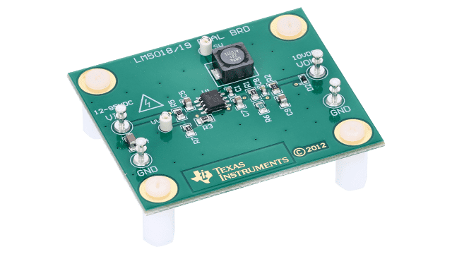
LM5018 Wide Vin Synchronous Buck Regulator Evaluation Board
Texas InstrumentsLM5018 Wide Vin Synchronous Buck Regulator Evaluation Board
Triple op amp evaluation module for SSOP-16 (non-inverting) package
Texas InstrumentsTriple op amp evaluation module for SSOP-16 (non-inverting) package

DAC39J82 Dual-Channel; 16-Bit; 2.8-GSPS; 1x-16x Interpolating Digital-to-Analog Converter EVM
Texas InstrumentsDAC39J82 Dual-Channel; 16-Bit; 2.8-GSPS; 1x-16x Interpolating Digital-to-Analog Converter EVM

Evaluation module for 2 battery cells to 3.3V, 100mA ultra-low operating current charge pump
Texas InstrumentsEvaluation module for 2 battery cells to 3.3V, 100mA ultra-low operating current charge pump
LMK00101 Ultra-low Jitter LVCMOS Fanout Buffer/Level Translator with Universal Input
Texas InstrumentsLMK00101 Ultra-low Jitter LVCMOS Fanout Buffer/Level Translator with Universal Input

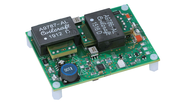
36 Volt Simple Switcher® Module 10A Demo Board
Texas Instruments36 Volt Simple Switcher® Module 10A Demo Board

High-Performance SMPTE Video Clock Module for Xilinx ML571 Serial Digital Video Board
Texas InstrumentsHigh-Performance SMPTE Video Clock Module for Xilinx ML571 Serial Digital Video Board
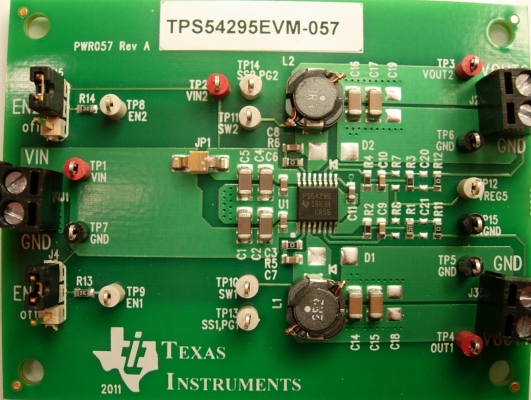
Evaluation Module for TPS54295 Synchronous Step-Down Converter
Texas InstrumentsEvaluation Module for TPS54295 Synchronous Step-Down Converter


LP8731YZREVM Dual High Current Step Down DC/DC and Dual Linear Regulators with I2C Interface EVM
Texas InstrumentsLP8731YZREVM Dual High Current Step Down DC/DC and Dual Linear Regulators with I2C Interface EVM

Dual Brushed DC Motor Gate Driver Evaluation Module
Texas InstrumentsDual Brushed DC Motor Gate Driver Evaluation Module

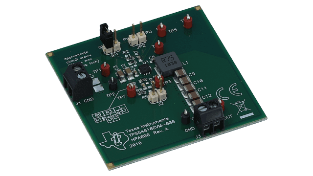
Evaluation Module for TPS54618 Synchronous Step-Down SWIFT™ DC/DC Converter
Texas InstrumentsEvaluation Module for TPS54618 Synchronous Step-Down SWIFT™ DC/DC Converter

1.25 Watt Fully Differential Audio Power Amplifier With RF Suppression and Shutdown
Texas Instruments1.25 Watt Fully Differential Audio Power Amplifier With RF Suppression and Shutdown


5A SIMPLE SWITCHER® Power Module with 36V Maximum Input Voltage Demo Board
Texas Instruments5A SIMPLE SWITCHER® Power Module with 36V Maximum Input Voltage Demo Board


