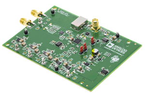
DC1846A-A
Analog Devices Inc.The LTC6947 is a high performance, low noise, 6GHz phase-locked loop (PLL), including a reference divider, phase-frequency detector (PFD), ultralow noise charge pump, fractional feedback divider, and VCO output divider.The fractional divider uses an advanced, 4th order ?? modulator which provides exceptionally low spurious levels. This allows wide loop bandwidths, producing extremely low integrated phase noise values.The programmable VCO output divider, with a range of 1 through 6, extends the output frequency range. The differential, low-noise output buffer has user-programmable output power ranging from ?4.3dBm to +4.5dBm, and may be muted through either a digital input pin or software.The ultralow noise charge pump contains selectable high and low voltage clamps useful for VCO monitoring, and also may be set to provide a V+/2 bias.All device settings are controlled through a SPI-compatible serial port.Applications Wireless Basestations (LTE, WiMAX, W-CDMA, PCS) Broadband Wireless Access Microwave Data Links Military and Secure Radio Test and Measurement
LTC2872 RS232/RS485 Dual Multiprotocol Transceiver with Integrated Termination
Analog Devices Inc.DC1851A: Demo Board for the LTC2872 RS232/RS485 Dual Multiprotocol Transceiver with Integrated Termination.
LTC3536EMSE (MSOP) Demo Board | 1.8V ≤ VIN ≤ 5.5V, VOUT = 3.3V @ 1A
Analog Devices Inc.Demonstration circuit 1852A is a combined step-up and step-down DC/DC converter, using the LTC3536 monolithic synchronous buck-boost regulator in the MSOP package. The DC1852A has wide input voltage range of 1.8V to 5.5V and is capable of delivering up to 1A of output current. The output voltage of the DC1852A can be set as low as 1.8V and can go as high as 5.5V. DC1852A supports two operation modes: fixed-frequency pulse-width modulation (PWM) and Burst Mode® operation.
DC1856B-B
Analog Devices Inc.The LTM4649 is a complete 10A high efficiency switching mode step-down DC/DC ?Module? regulator in a 9mm ? 15mm ? 4.92 BGA package. Included in the package are the switching controller, power FETs, inductor, and all support components. Operating over an input voltage range of 4.5V to 16V, the LTM4649 supports an output voltage range of 0.6V to 3.3V, set by a single external resistor. This high efficiency design delivers 10A continuous current. Only bulk input and output capacitors are needed.High switching frequency and a current mode architecture enable a very fast transient response to line and load changes without sacrificing stability. The device supports frequency synchronization, programmable multiphase operation, and output voltage tracking for supply rail sequencing.Fault protection features include output overvoltage and overcurrent protection. The LTM4649 is offered in a small 9mm ? 15mm ? 4.92mm BGA package available with SnPb or RoHS compliant terminal finish.Applications Telecom, Networking and Industrial Equipment Point of Load Regulation
DC1864A
Analog Devices Inc.The LTC3621/LTC3621-2 is a high efficiency 17V, 1A synchronous monolithic step-down regulator. The switching frequency is fixed to 1MHz or 2.25MHz with a ?40% synchronizing range. The regulator features ultralow quiescent current and high efficiencies over a wide VOUT range.The step-down regulator operates from an input voltage range of 2.7V to 17V and provides an adjustable output range from 0.6V to VIN while delivering up to 1A of output current. A user-selectable mode input is provided to allow the user to trade off ripple noise for light load efficiency; Burst Mode operation provides the highest efficiency at light loads, while pulse-skipping mode provides the lowest voltage ripple. The MODE pin can also be used to allow the user to sync the switching frequency to an external clock. LTC3621 Options Part Name Frequency VOUT LTC3621 1.00MHz Adjustable LTC3621-3.3 1.00MHz 3.3V LTC3621-5 1.00MHz 5V LTC3621-2 2.25MHz Adjustable LTC3621-23.3 2.25MHz 3.3 LTC3621-25 2.25MHz 5V APPLICATIONS Portable-Handheld Scanners Industrial and Embedded Computing Automotive Applications Emergency Radio
LT1374CR | 4.5A SWITCH, 500kHz STEP-DOWN REGULATOR, 5.5V to 25VIN, 3.3V or 5.0V @ 4A OUTPUT, DD PACKAGE
Analog Devices Inc.DC187A-A: Demo Board for the LT1374 4.5A, 500kHz Step-Down Switching Regulator.
DC1884A-C
Analog Devices Inc.The LTM9011-14/LTM9010-14/LTM9009-14 are 8-channel, simultaneous sampling 14-bit A/D converters designed for digitizing high frequency, wide dynamic range signals. AC performance includes 73.1dB SNR and 88dB spurious free dynamic range (SFDR). Low power consumption per channel reduces heat in high channel count applications. Integrated bypass capacitance and flow-through pinout reduces overall board space requirements.DC specs include ?1LSB INL (typ), ?0.3LSB DNL (typ) and no missing codes over temperature. The transition noise is a low 1.2LSBRMS.The digital outputs are serial LVDS to minimize the number of data lines. Each channel outputs two bits at a time (2-lane mode). At lower sampling rates there is a one bit per channel option (1-lane mode).The ENC+ and ENC? inputs may be driven differentially or single-ended with a sine wave, PECL, LVDS, TTL, or CMOS inputs. An internal clock duty cycle stabilizer allows high performance at full speed for a wide range of clock duty cycles.Applications Communications Cellular Base Stations Software Defined Radios Portable Medical Imaging Multichannel Data Acquisition Nondestructive Testing
LTM9006-14 | 14-Bit, 25Msps, 1.8V Octal Serial ADC, 1MHz < Ain < 70MHz, Requires DC1371 and DC1075
Analog Devices Inc.DC1884A-F: Demo Board for the LTM9006-14 14-Bit, 25Msps Low Power Octal ADCs.
LTC3639EMSE Demo Board | Sync Buck, 4V ≤ VIN ≤ 150V, VOUT = 1.8V/3.3V/5V/Adj @ 100mA
Analog Devices Inc.Demonstration circuit 1901A is a 150V input, 100mA output DC/DC power supply featuring the LTC3639. The IC operates in a high efficiency Burst Mode® operation and includes internal high and low side power MOSFETs. The board will accept an input voltage between 4V and 150V, and provide jumper selected output voltages of 1.8V, 3.3V, 5V and an option for additional voltages. The IC includes internal soft-start and a provision for increasing soft-start time.
DC1908A-B
Analog Devices Inc.The LTC2337-18 is a low noise, high speed 18-bit successive approximation register (SAR) ADC with fully differential inputs. Operating from a single 5V supply, the LTC2337-18 has a ?10.24V true bipolar input range, making it ideal for high voltage applications which require a wide dynamic range. The LTC2337-18 achieves ?4LSB INL maximum, no missing codes at 18-bits with 100dB SNR.The LTC2337-18 has an on-board single-shot capable reference buffer and low drift (20ppm/?C max) 2.048V temperature compensated reference. The LTC2337-18 also has a high speed SPI-compatible serial interface that supports 1.8V, 2.5V, 3.3V and 5V logic while also featuring a daisy-chain mode. The fast 500ksps throughput with no cycle latency makes the LTC2337-18 ideally suited for a wide variety of high speed applications. An internal oscillator sets the conversion time, easing external timing considerations. The LTC2337-18 dissipates only 35mW and automatically naps between conversions, leading to reduced power dissipation that scales with the sampling rate. A sleep mode is also provided to reduce the power consumption of the LTC2337-18 to 300?W for further power savings during inactive periods.Applications Programmable Logic Controllers Industrial Process Control High Speed Data Acquisition Portable or Compact Instrumentation ATE
DC1908A-F
Analog Devices Inc.The LTC2326-18 is a low noise, high speed 18-bit successive approximation register (SAR) ADC with pseudo-differential inputs. Operating from a single 5V supply, the LTC2326-18 has a ?10.24V true bipolar input range, making it ideal for high voltage applications which require a wide dynamic range. The LTC2326-18 achieves ?5LSB INL maximum, no missing codes at 18 bits with 95dB SNR.The LTC2326-18 has an onboard single-shot capable reference buffer and low drift (20ppm/?C max) 2.048V temperature compensated reference. The LTC2326-18 also has a high speed SPI-compatible serial interface that supports 1.8V, 2.5V, 3.3V and 5V logic while also featuring a daisy-chain mode. The fast 250ksps throughput with no cycle latency makes the LTC2326-18 ideally suited for a wide variety of high speed applications. An internal oscillator sets the conversion time, easing external timing considerations. The LTC2326-18 dissipates only 28mW and automatically naps between conversions, leading to reduced power dissipation that scales with the sampling rate. A sleep mode is also provided to reduce the power consumption of the LTC2326-18 to 300?W for further power savings during inactive periods. Bits LTC2326-16 16 LTC2326-18 18 Applications Programmable Logic Controllers Industrial Process Control High Speed Data Acquisition Portable or Compact Instrumentation ATE
DC1908A-H
Analog Devices Inc.The LTC2327-16 is a low noise, high speed 16-bit successive approximation register (SAR) ADC with pseudo-differential inputs. Operating from a single 5V supply, the LTC2327-16 has a ?10.24V true bipolar input range, making it ideal for high voltage applications which require a wide dynamic range. The LTC2327-16 achieves ?1.5LSB INL maximum, no missing codes at 16 bits with 93.5dB SNR.The LTC2327-16 has an on-board single-shot capable reference buffer and low drift (20ppm/?C max) 2.048V temperature compensated reference. The LTC2327-16 also has a high speed SPI-compatible serial interface that supports 1.8V, 2.5V, 3.3V and 5V logic while also featuring a daisy-chain mode. The fast 500ksps throughput with no cycle latency makes the LTC2327-16 ideally suited for a wide variety of high speed applications. An internal oscillator sets the conversion time, easing external timing considerations. The LTC2327-16 dissipates only 36mW and automatically naps between conversions, leading to reduced power dissipation that scales with the sampling rate. A sleep mode is also provided to reduce the power consumption of the LTC2327-16 to 300?W for further power savings during inactive periods. Bits LTC2327-16 16 LTC2327-18 18 Applications Programmable Logic Controllers Industrial Process Control High Speed Data Acquisition Portable or Compact Instrumentation ATE
LTC3553EUD-2 Demo Board I Micropower USB Power Manager with Li-Ion Charger, Always-On LDO and Buck Regulator
Analog Devices Inc.DC1920A: Demo Board for the LTC3553-2 - Micropower USB Power Manager with Li-Ion Charger, Always-On LDO and Buck Regulator
DC1922A
Analog Devices Inc.The LTC3129 is a high efficiency, 200mA buck-boost DC/DC converter with a wide VIN and VOUT range. It includes an accurate RUN pin threshold to allow predictable regulator turn-on and a maximum power point control (MPPC) capability that ensures maximum power extraction from non-ideal power sources such as photovoltaic panels.The LTC3129 employs an ultralow noise, 1.2MHz PWM switching architecture that minimizes solution footprint by allowing the use of tiny, low profile inductors and ceramic capacitors. Built-in loop compensation and soft-start simplify the design. For high efficiency operation at light loads, automatic Burst Mode operation can be selected, reducing the quiescent current to just 1.3?A.Additional features include a power good output, less than 10nA of shutdown current and thermal shutdown.The LTC3129 is available in thermally enhanced 3mm ? 3mm QFN and 16-lead MSOP packages. For fixed output voltage options, see the functionally equivalent LTC3129-1, which eliminates the need for an external feedback divider. Output Voltage LTC3129 Adjustable?1.4V to 15.75V via resistor divider LTC3129-1 8 pin programmable output voltages from 2.5V to 15V Applications Industrial Wireless Sensor Nodes Post-Regulator for Harvested Energy Solar Panel Post-Regulator/Charger Intrinsically Safe Power Supplies Wireless Microphones Avionics-Grade Wireless Headsets
LTC2376-20 Demo Board | 20-Bit, 250ksps, SAR ADC with 104dB SNR. Requires DC2026
Analog Devices Inc.The LTC2378-20, LTC2377-20 and LTC2376-20 are 20‑bit, low power, low noise SAR ADCs with serial outputs that operate from a single 2.5V supply. The demo manual refers to the LTC2378-20 but applies to all parts in the family, the only difference being the maximum sample rate. The LTC2378-20 supports a ±5V fully differential input range with a 104dB SNR, consumes only 21mW and achieves ±2ppm INL max with no missing codes at 20 bits. The DC1925A demonstrates the DC and AC performance of the LTC2378-20 in conjunction with the DC590 QuikEval™ and DC890 PScope™ data collection boards. Use the DC590 to demonstrate DC performance such as peak-to-peak noise and DC linearity.
DC1934A
Analog Devices Inc.The LTM8053 is a 40VIN, 3.5A continuous, 6A peak step-down ?Module? (power module) regulator. Included in the package are the switching controller, power switches, inductor, and all support components. Operating over an input voltage range of 3.4V to 40V, the LTM8053 / LTM8053- 1 supports an output voltage range of 0.97V to 15V and a switching frequency range of 200kHz to 3MHz, each set by a single resistor. Only the input and output filter capacitors are needed to finish the design. The LTM8053-1 can operate in forced continuous mode.The low profile package enables utilization of unused space on the bottom of PC boards for high density point of load regulation. The LTM8053 / LTM8053-1 is packaged in a thermally enhanced, compact over-molded ball grid array (BGA) package suitable for automated assembly by standard surface mount equipment. The LTM8053 / LTM8053-1 is RoHS compliant.APPLICATIONS Automotive Battery Regulation Power for Portable Products Distributed Supply Regulation Industrial Supplies Wall Transformer Regulation
DC1936A
Analog Devices Inc.The LTC3882 is a dual, PolyPhase DC/DC synchronous step-down switching regulator controller with PMBus compliant serial interface. It uses a constant frequency, leading-edge modulation, voltage mode architecture for excellent transient response and output regulation. Each PWM channel can produce output voltages from 0.5V to 5.25V using a wide range of 3.3V compatible power stages, including power blocks, DrMOS or discrete FET drivers. Up to four LTC3882s can operate in parallel for 2-, 3-, 4-, 6- or 8-phase operation.LTC3882 system configuration and monitoring is supported by the LTpowerPlay? software tool. The device?s serial interface can be used to read back input voltage, output voltage and current, temperature and fault status. A wide range of operating parameters can be set via the digital interface or stored in internal EEPROM for use at power up. Switching frequency and phase, output voltage and device address can also be programmed using external configuration resistors. PWM?Enable Output TG/BG Control HW?Write Protect Dedicated PGOOD Differential Vout Sense LTC3882 Yes Yes Yes No? VOUT0 Only LTC3882-1 ?No No No Yes VOUT0 & VOUT1 Applications High Current Distributed Power Systems Servers, Network and Storage Equipment Intelligent Energy Efficient Power Regulation Industrial/Telecom/ATE Systems
LT3799EMSE-1 Demo Board | Offline Isolated Flyback LED Driver with PFC
Analog Devices Inc.DC1947A: Demo Board for the LT3799-1 Offline Isolated Flyback LED Controller with Active PFC.
DC194A-A
Analog Devices Inc.The LT1317/LT1317B are micropower, fixed frequency step-up DC/DC converters that operate over a wide input voltage range of 1.5V to 12V. The LT1317 features automatic shifting to power saving Burst Mode? operation at light loads. High efficiency is maintained over a broad 300?A to 200mA load range. Peak switch current during Burst Mode operation is kept below 250mA for most operating conditions which results in low output ripple voltage, even at high input voltages. The LT1317B does not shift into Burst Mode operation at light loads, eliminating low frequency output ripple at the expense of light load efficiency.The LT1317/LT1317B contain an internal low-battery detector with a 200mV reference that stays alive when the device goes into shutdown.No-load quiescent current of the LT1317 is 100?A and shuts down to 30?A. The internal NPN power switch handles a 500mA current with a voltage drop of just 300mV.The LT1317/LT1317B are available in MS8 and SO-8 packages.Applications Cellular Telephones Cordless Telephones Pagers GPS Receivers Battery Backup Portable Electronic Equipment Glucose Meters Diagnostic Medical Instrumentation
LTC3374EUHF Demo Board 8-Channel Parallelable 1A Buck DC/DC
Analog Devices Inc.Demonstration circuit 1953A is an 8-output power supply featuring the LTC3374. The LTC3374 has eight synchronous buck regulators each with an independent VIN supply. Up to four buck regulators may be paralleled together to create a higher power buck regulator with a single inductor. The input range of the LTC3374 is ideal for single cell Li-Ion/Polymer battery applications. The buck regulators can be enabled via external precision threshold enable pins to allow hardwired power up sequences.


