Top Manufacturers
Stock

Displaying 1981 - 2000 of 5440

Evaluation Kits from Analog Devices Inc.

AD9508/PCBZ

Analog Devices Inc.
The AD9508 provides clock fanout capability in a design thatemphasizes low jitter to maximize system performance. Thisdevice benefits applications like clocking data converters withdemanding phase noise and low jitter requirements.There are four independent differential clock outputs, each withvarious types of logic levels available. Available logic typesinclude LVDS (1.65 GHz), HSTL (1.65 GHz), and 1.8 V CMOS(250 MHz). In 1.8 V CMOS output mode, the differential outputbecomes two CMOS single-ended signals. The CMOS outputsare 1.8 V logic levels, regardless of the operating supply voltage.Each output has a programmable divider that can be bypassedor be set to divide by any integer up to 1024. In addition, theAD9508 supports a coarse output phase adjustment betweenthe outputs.The device can also be pin programmed for various fixedconfigurations at power-up without the need for SPI or I2C programming.The AD9508 is available in a 24-lead LFCSP and operates froma either a single 2.5 V or 3.3 V supply. The temperature range is?40?C to +85?C.Applications Low jitter, low phase noise clock distribution Clocking high speed ADCs, DACs, DDSs, DDCs, DUCs, MxFEs High performance wireless transceivers High performance instrumentation Broadband infrastructure

AD9517-1A/PCBZ

Analog Devices Inc.
The AD9517-11?provides a multi-output clock distribution function with subpicosecond jitter performance, along with an on-chip PLL and VCO. The on-chip VCO tunes from 2.30 GHz to 2.65 GHz. Optionally, an external VCO/VCXO of up to 2.4 GHz can be used.The AD9517-1 emphasizes low jitter and phase noise to maximize data converter performance, and it can benefit other applications with demanding phase noise and jitter requirements.The AD9517-1 features four LVPECL outputs (in two pairs) and four LVDS outputs (in two pairs). Each LVDS output can be reconfigured as two CMOS outputs. The LVPECL outputs operate to 1.6 GHz, the LVDS outputs operate to 800 MHz, and the CMOS outputs operate to 250 MHz.For applications that require additional outputs, a crystal reference input, zero-delay, or EEPROM for automatic configuration at startup, the AD9520 and AD9522 are available. In addition, the AD9516 and AD9518 are similar to the AD9517 but have a different combination of outputs.Each pair of outputs has dividers that allow both the divide ratio and coarse delay (or phase) to be set. The range of division for the LVPECL outputs is 1 to 32. The LVDS/CMOS outputs allow a range of divisions up to a maximum of 1024.The AD9517-1 is available in a 48-lead LFCSP and can be operated from a single 3.3 V supply. An external VCO, which requires an extended voltage range, can be accommodated by connecting the charge pump supply (VCP) to 5 V. A separate LVPECL power supply can be from 2.5 V to 3.3 V (nominal).The AD9517-1 is specified for operation over the industrial range of ?40?C to +85?C.Applications Low jitter, low phase noise clock distribution 10/40/100 Gb/sec networking line cards, including SONET, Synchronous Ethernet, OTU2/3/4 Forward error correction (G.710) Clocking high speed ADCs, DACs, DDSs, DDCs, DUCs, MxFEs High performance wireless transceivers ATE and high performance instrumentation 1AD9517 is used throughout the data sheet to refer to all the members of the AD9517 family. However, when AD9517-1 is used, it is refers to that specific member of the AD9517 family.

AD9530/PCBZ

Analog Devices Inc.
The AD9530 is a fully integrated PLL and distribution supporting, clock cleanup, and frequency translation device for 40 Gbps/ 100 Gbps OTN applications. The internal PLL can lock to one of two reference frequencies to generate four discrete output frequencies up to 2.7 GHz.The AD9530 features an internal 5.11 GHz to 5.4 GHz, ultralow noise voltage controlled oscillator (VCO). All four outputs are individually divided down from the internal VCO using two high speed VCO dividers (the Mx dividers) and four individual 8-bit channel dividers (the Dx dividers). The high speed VCO dividers offer fixed divisions of 2, 2.5, 3, and 3.5 for wide coverage of possible output frequencies. The AD9530 is configurable for loop bandwidths

AD9549A/PCBZ

Analog Devices Inc.
The AD9549 provides synchronization for many systems, including synchronous optical networks (SONET/SDH). The AD9549 generates an output clock, synchronized to one of two external input references. The external references may contain significant time jitter, also specified as phase noise. Using a digitally controlled loop and holdover circuitry, the AD9549 continues to generate a clean (low jitter), valid output clock during a loss of reference condition, even when both references have failed.The AD9549 operates over an industrial temperature range of ?40?C to +85?C.APPLICATIONS Network synchronization Reference clock jitter cleanup SONET/SDH clocks up to OC-192, including FEC Stratum 3/3E reference clocks Wireless base stations, controllers Cable infrastructure Data communications

AD9550/PCBZ

Analog Devices Inc.
The AD9550 is a phase-locked loop (PLL) based clock translatordesigned to address the needs of wireline communicationand base station applications. The device employs an integer-NPLL to accommodate the applicable frequency translationrequirements. It accepts a single-ended input reference signalat the REF input.The AD9550 is pin programmable, providing a matrix ofstandard input/output frequency translations from a list of15 possible input frequencies to a list of 51 possible outputfrequency pairs (OUT1 and OUT2).The AD9550 output is compatible with LVPECL, LVDS, orsingle-ended CMOS logic levels, although the AD9550 isimplemented in a strictly CMOS process.The AD9550 operates over the extended industrial temperaturerange of ?40?C to +85?C.APPLICATIONS Cost effective replacement of high frequency VCXO, OCXO, and SAW resonators Flexible frequency translation for wireline applications such as Ethernet, T1/E1, SONET/SDH, GPON, xDSL Wireless infrastructure Test and measurement (including handheld devices)

AD9554/PCBZ

Analog Devices Inc.
The AD9554 is a low loop bandwidth clock translator that provides jitter cleanup and synchronization for many systems, including synchronous optical networks (SONET/SDH). The AD9554 generates an output clock synchronized to up to four external input references. The digital PLL (DPLL) allows for reduction of input time jitter or phase noise associated with the external references. The digitally controlled loop and holdover circuitry of the AD9554 continuously generates a low jitteroutput clock even when all reference inputs have failed.The AD9554 operates over an industrial temperature range of ?40?C to +85?C. If a smaller device is needed, the AD9554-1 is a version of this device with one output per PLL. If a single or dual DPLL version of this device is needed, refer to the AD9557 or AD9559, respectively.Applications Network synchronization, including synchronous Ethernet and synchronous digital hierarchy (SDH) to optical transport network (OTN) mapping/demapping Cleanup of reference clock jitter SONET/SDH clocks up to OC-192, including FEC Stratum 3 holdover, jitter cleanup, and phase transient control Cable infrastructure Data communications Professional video

AD9572-EVALZ-LVD

Analog Devices Inc.
The AD9572 provides a multioutput clock generator function along with two on-chip PLL cores, optimized for fiber channel line card applications that include an Ethernet interface. The integer-N PLL design is based on the Analog Devices, Inc., proven portfolio of high performance, low jitter frequencysynthesizers to maximize network performance. Other applications with demanding phase noise and jitter requirements also benefit from this part. The PLL section consists of a low noise phase frequency detector (PFD), a precision charge pump (CP), a low phase noise voltage controlled oscillator (VCO), and a preprogrammed feedback divider and output divider. By connecting an external crystal or reference clock to the REFCLK pin, frequencies up to 156.25 MHz can be locked to the input reference. Each output divider and feedback divider ratio is preprogrammed for therequired output rates. A second PLL also operates as an integer-N synthesizer anddrives two LVPECL or LVDS output buffers for 106.25 MHzoperation. No external loop filter components are required, thusconserving valuable design time and board space. The AD9572 is available in a 40-lead, 6 mm ? 6 mm lead framechip scale package (LFCSP) and can be operated from a single3.3 V supply. The temperature range is ?40?C to +85?C.APPLICATIONSFiber channel line cards, switches, and routersGigabit Ethernet/PCIe support included Low jitter, low phase noise clock generation

AD9575-EVALZ-LVD

Analog Devices Inc.
The AD9575 provides a highly integrated, dual output clockgenerator function including an on-chip PLL core that isoptimized for network clocking. The integer-N PLL design isbased on the Analog Devices, Inc., proven portfolio of high performance, low jitter frequency synthesizers to maximize linecard performance. Other applications with demanding phasenoise and jitter requirements also benefit from this part.The PLL section consists of a low noise phase frequency detector (PFD), a precision charge pump, a low phase noise voltagecontrolled oscillator (VCO), and pin selectable feedback and output dividers.By connecting an external crystal, popular network output frequencies can be locked to the input reference. The output divider and feedback divider ratios are pin programmable for therequired output rates. No external loop filter components are required, thus conserving valuable design time and board space.The AD9575 is available in a 16-lead, 4.4 mm ? 5.0 mm TSSOP and can be operated from a single 3.3 V supply. The temperature range is ?40?C to +85?C. APPLICATIONS GbE/FC/SONET line cards, switches, and routers CPU/PCI-E applications Low jitter, low phase noise clock generation

AD9629-80EBZ

Analog Devices Inc.
The AD9629 is a monolithic, single channel 1.8 V supply, 12-bit, 20 MSPS/40 MSPS/65MSPS/80 MSPS analog-to-digital converter (ADC). It features a high performance sample-and-hold circuit and on-chip voltage reference.The product uses multistage differential pipeline architecture with output error correction logic to provide 12-bit accuracy at 80 MSPS data rates and to guarantee no missing codes over the full operating temperature range.The ADC contains several features designed to maximize flexibility and minimize system cost, such as programmable clock and data alignment and programmable digital test pattern generation. The available digital test patterns include built-in deterministic and pseudorandom patterns, along with custom user-defined test patterns entered via the serial port interface (SPI).A differential clock input with optional 1, 2, or 4 divide ratios controls all internal conversion cycles.The digital output data is presented in offset binary, gray code, or twos complement format. A data output clock (DCO) is provided to ensure proper latch timing with receiving logic. Both 1.8 V and 3.3 V CMOS levels are supported.The AD9629 is available in a 32-lead RoHS compliant LFCSP and is specified over the industrial temperature range (?40?C to +85?C).Applications Communications Diversity radio systems Multimode digital receivers GSM, EDGE, W-CDMA, LTE, CDMA2000, WiMAX, TD-SCDMA Smart antenna systems Battery-powered instruments Hand held scope meters Portable medical imaging Ultrasound Radar/LIDAR PET/SPECT imagingProduct Highlights1. The AD9629 operates from a single 1.8 V analog power supply and features a separate digital output driver supply to accommodate 1.8 V to 3.3 V logic families.2. The sample-and-hold circuit maintains excellent performance for input frequencies up to 200 MHz and is designed for low cost, low power, and ease of use.3. A standard serial port interface (SPI) supports various product features and functions, such as data output formatting, internal clock divider, power-down, DCO and data output (D11 to D0) timing and offset adjustments, and voltage reference modes.4. The AD9629 is packaged in a 32-lead RoHS compliant LFCSP that is pin compatible with the AD9609 10-bit ADC and the AD9649 14-bit ADC, enabling a simple migration path between 10-bit and 14-bit converters sampling from 20 MSPS to 80 MSPS.

DC918C-K

Analog Devices Inc.
The LTC2207-14/LTC2206-14 are 105Msps/80Msps, sampling 14-bit A/D converters designed for digitizing high frequency, wide dynamic range signals up to input frequencies of 700MHz. The input range of the ADC can be optimized with the PGA front end.The LTC2207-14/LTC2206-14 are perfect for demanding communications applications, with AC performance that includes 77.3dB SNR and 98dB spurious free dynamic range (SFDR). Ultralow jitter of 80fsRMS allows undersampling of high input frequencies with excellent noise performance. Maximum DC specs include ?1.5LSB INL, ?1LSB DNL (no missing codes) over temperature.A separate output power supply allows the CMOS output swing to range from 0.5V to 3.6V.The ENC+ and ENC? inputs may be driven differentially or single-ended with a sine wave, PECL, LVDS, TTL or CMOS inputs. An optional clock duty cycle stabilizer allows high performance at full speed with a wide range of clock duty cycles. Bits LTC2206-14 14 LTC2206-16 16 Applications Telecommunications Receivers Cellular Base Stations Spectrum Analysis Imaging Systems ATE

LTC3452EUF Demo Board

Analog Devices Inc.
DC928A: Demo Board for the LTC3452 Synchronous Buck-Boost MAIN/CAMERA White LED Driver.

DC939A

Analog Devices Inc.
The LTC2484 combines a 24-bit No Latency ??? analog-to-digital converter with patented Easy Drive? technology. The patented sampling scheme eliminates dynamic input current errors and the shortcomings of on-chip buffering through automatic cancellation of differential input current. This allows large external source impedances and input signals with rail-to-rail input range to be directly digitized while maintaining exceptional DC accuracy.The LTC2484 includes an on-chip oscillator. The LTC2484 can be configured to reject line frequencies. 50Hz, 60Hz or simultaneous 50Hz/60Hz line frequency rejection can be selected as well as a 2? speed-up mode.The LTC2484 allows a wide common mode input range (0V to VCC) independent of the reference voltage. The reference can be as low as 100mV or can be tied directly to VCC. The LTC2484 includes an on-chip trimmed oscillator, eliminating the need for external crystals or oscillators. Absolute accuracy and low drift are automatically maintained through continuous, transparent, offset and full-scale calibration.Applications Direct Sensor Digitizer Weight Scales Direct Temperature Measurement Strain Gauge Transducers Instrumentation Industrial Process Control DVMs and Meters

LT3740EDHC Demo Board

Analog Devices Inc.
DC947A: Demo Board for the LT3740 Wide Operating Range, Valley Mode, No RSENSE Synchronous Step-Down Controller.

DC949A-B

Analog Devices Inc.
The LT3478/LT3478-1 are 4.5A step-up DC/DC converters designed to drive LEDs with a constant current over a wide programmable range. Series connection of the LEDs provides identical LED currents for uniform brightness without the need for ballast resistors and expensive factory calibration.The LT3478-1 reduces external component count and cost by integrating the LED current sense resistor. The LT3478 uses an external sense resistor to extend the maximum programmable LED current beyond 1A and also to achieve greater accuracy when programming low LED currents. Operating frequency can be set with an external resistor from 200kHz up to 2.25MHz. Unique circuitry allows a PWM dimming range up to 3000:1 while maintaining constant LED color. The LT3478/LT3478-1 are ideal for high power LED driver applications such as automotive TFT LCD backlights, courtesy lighting and heads-up displays. One of two CTRL pins can be used to program maximum LED current. The other CTRL pin can be used to program a reduction in maximum LED current vs temperature to maximize LED usage and improve reliability.Additional features include inrush current protection, programmable open LED protection and programmable soft-start. Each part is available in a 16-pin thermally enhanced TSSOP Package.Applications High Power LED Driver Automotive Lighting

LTC3810EG Demo Board | 13V ≤ VIN ≤ 80V; VOUT = 12V @ 6A

Analog Devices Inc.
Demonstration circuit 952 is a current mode synchronous switching regulator featuring the LTC3810. The circuit is configured as a synchronous step-down regulator operating at 230kHz switching frequency. Output voltage is 12V at 6A maximum load. The input voltage range is 13V to 80V.

LTC3824EMSE Demo Board | 5.5V ≤ VIN ≤ 60V, VOUT: 5V/2A

Analog Devices Inc.
Demonstration circuit 960 is a high voltage, current-mode DC/DC step-down controller featuring the LTC3824 in a small 10-pin MSOP package. The board operates from an input voltage of 5.5V to 60V and outputs 5V @ 2A. The converter uses a P-channel MOSFET for the main switch resulting in a low parts count design. Operating frequency is set to 200kHz with the option to accept a synchronized external clock.

LT6600-2.5 Frequency (Fc) = 2.5MHz

Analog Devices Inc.
DC962A-A: Demo Board for LT6600-2.5 Very Low Noise, Differential Amplifier and 2.5MHz Lowpass Filter.

LTC3835EGN-1 Demo Board | 4.5V ≤ VIN ≤ 36V, VOUT = 3.3V @ 5A

Analog Devices Inc.
Demonstration circuit 965A is a single output high frequency step-down DC/DC converter featuring the low quiescent current LTC3835-1 in a 16-pin narrow SSOP package. The DC965A is programmed to generate a regulated 3.3V@5A output from a 4.5V to 36V input voltage. The LTC3835-1 is similar to the LTC3835 but has reduced functionality (it does not have PGOOD, ExtVCC or CLOCKOUT pins).

LT1952EGN-1, LTC3900CS8, LT4430ES6 Demo Board | VIN = 34V-75V VOUT = 3.3V @ 30A

Analog Devices Inc.
DC968A-A Demo Board for: LT1952 Single Switch Synchronous Forward Controller LTC3900 Synchronous Rectifier Driver for Forward Converters LT4430 Secondary-Side Optocoupler Driver

Displaying 1981 - 2000 of 5440

Latest Parts

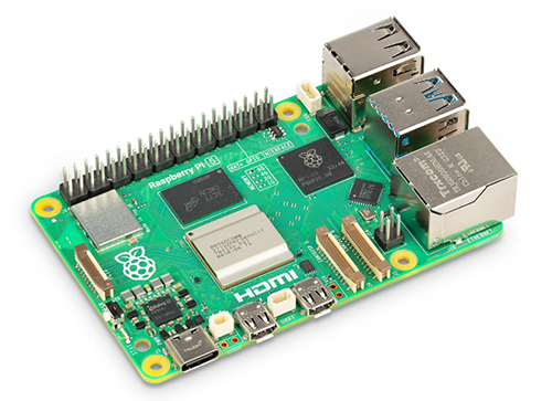
SC1112

Raspberry Pi

$80.00 - $80.01

IN STOCK 4808
Buy

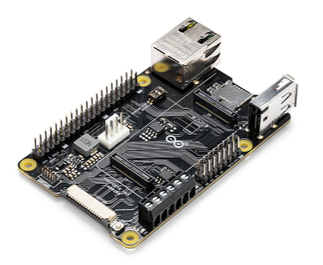
ASX00049

Arduino

* $33.68 - * $42.35

IN STOCK 3002
Buy
IN STOCK 4682
Buy

Reference Designs

RD006

Wurth Elektronik

RD006 - 3 W Dual-output isolated auxiliary supply for communication interfaces and measurement systems

CN0583

Analog Devices Inc.

Multistandard Micropower Verified Smoke Detection System-on-Module

Technical Resources

EVALUATION KITS

EVAL-AD7124-8SDZ

Analog Devices Inc.

$63.71 - * $75.61

IN STOCK 794
Buy
View All