
113589-HMC3587LP3B
Analog Devices Inc.The HMC3587LP 3BE is a HBT Gain Block MMI C amplifier covering 4 GHz to 10 GHz and packaged in a 3x3 mm plastic QFN SM T package. This versatile amplifier can be used as a cascadable IF or RF gain stage in 50 Ohm applications. The HMC3587LP 3BE delivers 14.5 dB gain, and +13 dBm output P1dB with only 3.5 dB noise figure.Applications Cellular / PCS / 3G Fixed Wireless & WLAN CATV, Cable Modem & DBS Microwave Radio & Test Equipment IF & RF Applications

115556-HMC561LP3
Analog Devices Inc.The HMC561LP3(E) is a x2 active broadband frequency multiplier utilizing GaAs PHEMT technology in a leadless RoHS compliant SMT package. When driven by a +5 dBm signal, the multiplier provides +14 dBm typical output power from 8 to 21 GHz and the Fo and 3Fo isolations are 15 dBc at 16 GHz. The HMC561LP3(E) is ideal for use in LO multiplier chains for Pt to Pt & VSAT Radios yielding reduced parts count vs. traditional approaches.The low additive SSB Phase Noise of -139 dBc/Hz at 100 kHz offset helps maintain good system noise performance. The RoHS packaged HMC561LP3(E) eliminates the need for wire bonding, and allows the use of surface mount manufacturing techniques.APPLICATIONS Clock Generation Applications:? SONET OC-192 & SDH STM-64? Point-to-Point & VSAT Radios? Test Instrumentation? Military & Space

115585-HMC680LP4
Analog Devices Inc.The HMC680LP4(E) is a digitally controlled variable gain amplifier which operates from 30 to 400 MHz, and can be programmed to provide -4 dB to +19 dB of gain, in 1 dB steps. The HMC680LP4(E) delivers noise figure of 5 dB in its maximum gain state, with output IP3 of up to +40 dBm in any state. This high linearity DVGA also provides a differential RF output which can be used to interface directly with SAW filters in Tx and Rx applications, and with digital to analog converters in Rx chains. The HMC680LP4(E) is housed in a RoHS compliant 4x4 mm QFN leadless package, and is CMOS/ TTL compatible.Applications Cellular/3G Infrastructure WiBro / WiMAX / 4G Microwave Radio & VSAT Test Equipment and Sensors IF & RF Applications?

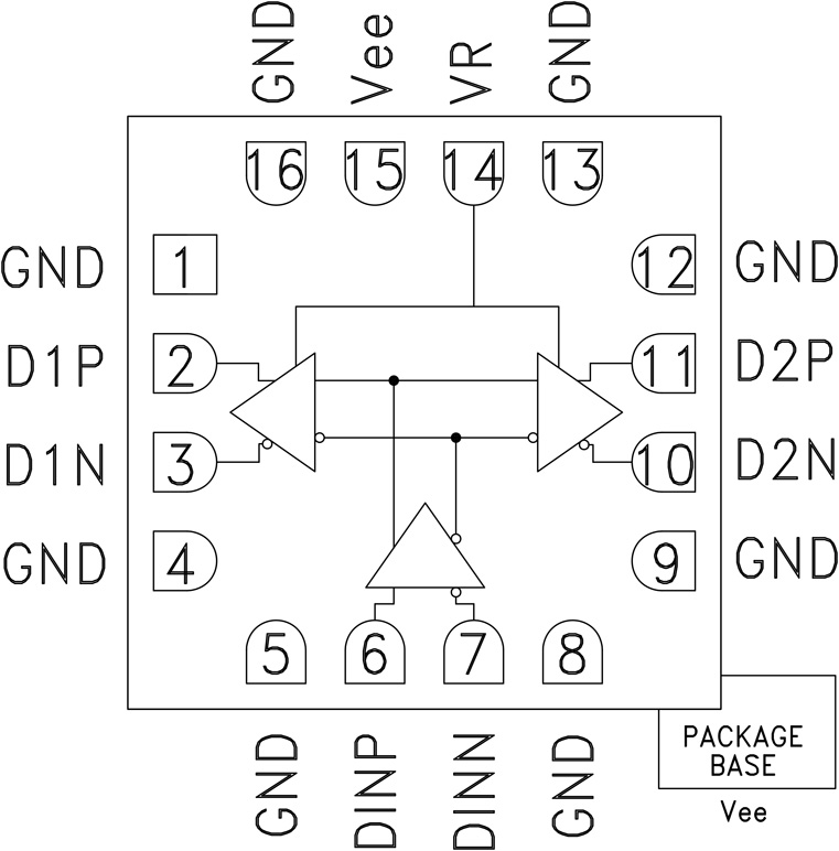
118777-HMC678LC3C
Analog Devices Inc.The HMC678LC3C is a 2:1 Selector designed to support data transmission rates of up to 13 Gbps, and selector port operation of up to 13 GHz. The selector routes one of the two single-ended inputs to the differential output upon assertion of the proper select port. All single-ended input signals to the HMC678LC3C are terminated with 50 ohms to ground on-chip, and may be either AC or DC coupled.The outputs of the HMC678LC3C may be operated either differentially or single-ended. Outputs can be connected directly to a 50 ohm terminated system, while DC blocking capacitors may be used if the terminating system is 50 ohms to a non-ground DC voltage. The HMC678LC3C operates from a single -3.3V dc supply and is available in a ceramic RoHS compliant 3x3 mm SMT package.APPLICATIONS 2:1 Multiplexer up to 13 Gbps RF ATE Applications Broadband Test & Measurement Serial Data Transmission up to 13 Gbps Redundant Path Switching Built-in Test
118777-HMC720LP3E
Analog Devices Inc.The HMC720LP3E is a 1:2 Fanout Buffer designed to support data transmission rates up to 14 Gbps, and clock frequencies as high as 14 GHz.All differential inputs to the HMC720LP3E are CML and terminated on-chip with 50 Ohms to the positive supply, GND, and may be DC or AC coupled. Outputs can be connected directly to a 50 Ohm ground-terminated system or drive devices with CML logic input. The HMC720LP3E also features an ouput level control pin, VR, which allows for loss compensation or signal level optimization. The HMC720LP3E operates from a single -3.3 V supply and is available in ROHS-compliant 3x3 mm SMT package.?APPLICATIONS 16 G Fiber Channel RF ATE Applications Broadband Test & Measurement Serial Data Transmission?up to 13 Gbps Clock Buffering up to 13 GHz

120257-HMC613LC4B
Analog Devices Inc.The HMC613LC4B is a Successive Detection Log Video Amplifier (SDLVA) which operates from 0.1 to 20 GHz. The HMC613LC4B provides a logging range of 59 dB. This device offers typical fast rise/fall times of 4/18 ns and a superior delay time of 14 ns. The HMC613LC4B log video output slope is typically 14 mV/dB. Maximum recovery times are less than 30 ns. The HMC613LC4B is available in a highly compact 4x4 mm SMT ceramic package and is ideal for high speed channelized receiver applications.APPLICATIONS EW, ELINT & IFM Receivers DF Radar Systems ECM Systems Broadband Test & Measurement Power Measurement & Control Circuits Military & Space Applications

122520-HMC724LC3
Analog Devices Inc.The HMC724 is a 1:2 Fanout Buffer designed to support data transmission rates up to 14 Gbps, and clock frequencies as high as 14 GHz. All differential inputs and outputs are DC coupled and terminated on chip with 50 Ohm resistors to ground. The outputs may be used in either single ended or differential modes, and should be AC or DC coupled into 50 Ohm resistors connected to ground.All differential inputs to the HMC724 are CML and terminated on-chip with 50 Ohms to the positive supply, GND, and may be DC or AC coupled. The differential CMl outputs are source terminated to to 50 Ohms and may also be AC or DC coupled. Outputs can be connected directly to a 50 Ohm ground-terminated system or drive devices with CML logic input. The HMC724 operates from a single -3.3 V supply and is available in ROHS-compliant 3x3 mm SMT package.APPLICATIONS 16 G Fiber Channel RF ATE Applications Broadband Test & Measurement Serial Data Transmission up to 14 Gbps Clock Buffering up to 14 GHz

122520-HMC727LC3C
Analog Devices Inc.The HMC727 is a D-type Flip Flop designed to support data transmission rates of up to 13 Gbps, and clock frequencies as high as 13 GHz. During normal operation, data is transferred to the outputs on the positive edge of the clock. Reversing the clock inputs allows for negative-edge triggered applications. All input signals to the HMC727 are terminated with 50 Ohms to ground on-chip, and maybe either AC or DC coupled.The differential outputs of the HMC727 may be either AC or DC coupled. Outputs can be connected directly to a 50 Ohm to ground terminated system, while DC blocking capacitors may be used if the terminating system is 50 Ohms to a nonground DC voltage. The HMC727 operates from a single -3.3V DC supply and is available in a ceramic RoHS compliant 3x3 mm SMT package.APPLICATIONS RF ATE Applications Broadband Test & Measurement Serial Data Transmission?up to 13 Gbps Digital Logic Systems up to 13 GHz

123987-HMC737LP4
Analog Devices Inc.The HMC737 is a GaAs InGaP Heterojunction Bipolar Transistor (HBT) MMIC VCO. The HMC737 integrate a resonator, negative resistance device, varactor diode and feature half frequency output. The VCO's phase noise performance is excellent over temperature, shock, and process due to the oscillator's monolithic structure. Power output is +9 dBm typical from a +4.2V supply voltage. The voltage controlled oscillator is packaged in a leadless QFN 4x4 mm surface mount package, and requires no external matching components.APPLICATIONS Point-to-Multi-Point Radios Test Equipment & Industrial Controls SATCOM Military End-Use

124390-HMC740ST89E
Analog Devices Inc.The HMC740 is an InGaP Heterojunction Bipolar Transistor (HBT) Gain Block MMIC SMT amplifier covering 0.05 to 3 GHz. Packaged in an industry standard SOT89, the amplifier can be used as a cascadable 50 Ohm RF or IF gain stage as well as a PA or LO driver with up to +18 dBm output power. The HMC740 offers 15 dB of gain with a +40 dBm output IP3 at 100 MHz, and can operate directly from a +5V supply. The HMC740 exhibits excellent gain and output power stability over temperature, while requiring a minimal number of external bias components.Applications Cellular/3G & WiMAX/4G Fixed Wireless & WLAN CATV, Cable Modem & DBS Microwave Radio & Test Equipment IF & RF Applications

125658-HMC686LP4
Analog Devices Inc.The HMC686LP4(E) is a high dynamic range passive MMIC mixer with integrated LO amplifier in a 4x4 SMT QFN package covering 0.7 to 1.1 GHz. Excellent input IP3 performance of +34 dBm for down conversion is provided for 3G & 4G GSM/CDMA applications at an LO drive of 0 dBm. With an input 1 dB compression of +25 dBm, the RF port will accept a wide range of input signal levels. Conversion loss is 7.5 dB typical. The DC to 500 MHz IF frequency response will satisfy GSM/CDMA transmit or receive frequency plans.The HMC686LP4(E) is optimized to high side LO frequency plans for 0.7 - 1.1 GHz RF Band and is pin for pin compatible with the?HMC684LP4(E)?which is a 0.7 - 1.0 GHz converter optimized for low side LO. The HMC686LP4(E) is optimized to low side LO frequency plans for 1.4 - 1.5 GHz RF LTE band applications.APPLICATIONS Cellular/3G & LTE/WiMAX/4G Basestations & Repeaters GSM, CDMA & OFDM Transmitters and Receivers

126578-HMC854LC5
Analog Devices Inc.The HMC854LC5 is a 4:1 multiplexer designed for 28 Gbps data serialization. The mux latches the four differential inputs on a rising edge of the input clock. The device uses both rising and falling edges of the half-rate clock to serialize the data. A quarter-rate clock output generated on chip can be used to synchronize data into the mux. The mux is DC coupled supporting broadband operation.All clock and data inputs to the HMC854LC5 are CML and terminated on-chip with 50 Ohms to the positive supply, GND, and may be DC or AC coupled. The differential outputs are source terminated to 50 Ohms and may also be AC or DC coupled. Outputs can be connected directly to a 50 Ohm ground terminated system, or drive devices with CML logic input. The HMC854LC5 also features an output level control pin, VR, which allows for loss compensation or signal level optimization. The HMC854LC5 operates from a single -3.3V supply and is available in ROHS compliant 5x5 mm SMT package.APPLICATIONS SONET OC-192 Broadband Test & Measurement Serial Data Transmission?up to 28 Gbps Mux Modes: 4:1 @ 28 Gbps NRZ 2:1 @ 14 Gbps RZ and NRZ FPGA Interfacing

ADP1048-600-EVALZ
Analog Devices Inc.The?ADP1047?/ ADP1048 are digital power factor correction (PFC) controllers that provide accurate input power metering capability and inrush current control for ac/dc systems. The ADP1047 is designed for single phase PFC applications; the ADP1048 is designed especially for interleaved and bridgeless PFC applications.The digital PFC function is based on a conventional boost PFC with multiplication of the output voltage feedback combined with the input current and voltage to provide optimum harmonic correction and power factor for ac/dc systems. All signals are converted into the digital domain to provide maximum flexibility; all key parameters can be reported and adjusted via the PMBus? interface. The ADP1047 / ADP1048 allow users to optimize system performance, maximize efficiency across the load range, and reduce design time to market.The ADP1047 / ADP1048 provide accurate rms measurement of input voltage, current, and power. This information can be reported to the microcontroller of the power supply via thePMBus interface.APPLICATIONS AC/DC power supplies for applications Computing Server & Storage Network and communication infrastructure Industrial and Medical

ADP1074-EVALZ
Analog Devices Inc.The ADP1074 is a current mode, fixed frequency, active clamp, synchronous forward controller designed for isolated dc to dc power supplies. Analog Devices proprietary iCouplers? are integrated in the ADP1074 to eliminate the bulky signal transformers and optocouplers that transmit signals over the isolation boundary. Integrating the iCouplers reduces system design complexity, cost, and component count and improves overall system reliability. With the integrated isolators and metal-oxide semiconductor field effect transistor (MOSFET) drivers on both the primary and the secondary side, the ADP1074 offers a compact system level design and yields a higher efficiency than a non-synchronous forward converter at heavy loads.The primary side pins provide functions for programming the switching frequency, maximum duty cycle, external frequency synchronization, and slope compensation.The secondary side pins provide functions for differential output voltage sensing, overvoltage, power good, tracking, and programmable light load mode setting.The feedback signal and timing of synchronous rectifier pulse-width modulations (PWMs) are transmitted from primary to secondary or from secondary to primary sides through the iCouplers using a proprietary transmission scheme.The ADP1074 also offers features such as input current protection, undervoltage lockout (UVLO), precision enable with adjustable hysteresis, overtemperature protection (OTP), and power saving light load mode (LLM).Applications Isolated dc-to-dc power conversion Intermediate bus voltage generation Telecom, industrial Base station and antenna RF power Small cell PoE powered device Enterprise switches/routers Core/edge/metro/optical routing Power modules

ADP121CB-1.2-EVALZ
Analog Devices Inc.The ADP121 is a quiescent current, low dropout, linear regulator that operates from 2.3 V to 5.5 V and provides up to 150 mA of output current. The low 135 mV dropout voltage at 150 mA load improves efficiency and allows operation over a wide input voltage range. The low 30 ?A of quiescent current at full load makes the ADP121 ideal for battery-operated portable equipment.The ADP121 is available in output voltages ranging from 1.2 V to 3.3 V. The parts are optimized for stable operation with small 1 ?F ceramic output capacitors. The ADP121 delivers good transient performance with minimal board area.Short-circuit protection and thermal overload protection circuits prevent damage in adverse conditions. The ADP121 is available in a tiny 5-lead TSOT and 4-ball 0.4 mm pitch WLCSP pack-ages and utilizes the smallest footprint solution to meet a variety of portable applications.
ADP121CB-2.0-EVALZ
Analog Devices Inc.The ADP121 is a quiescent current, low dropout, linear regulator that operates from 2.3 V to 5.5 V and provides up to 150 mA of output current. The low 135 mV dropout voltage at 150 mA load improves efficiency and allows operation over a wide input voltage range. The low 30 ?A of quiescent current at full load makes the ADP121 ideal for battery-operated portable equipment.The ADP121 is available in output voltages ranging from 1.2 V to 3.3 V. The parts are optimized for stable operation with small 1 ?F ceramic output capacitors. The ADP121 delivers good transient performance with minimal board area.Short-circuit protection and thermal overload protection circuits prevent damage in adverse conditions. The ADP121 is available in a tiny 5-lead TSOT and 4-ball 0.4 mm pitch WLCSP pack-ages and utilizes the smallest footprint solution to meet a variety of portable applications.
ADP121CB-3.3-EVALZ
Analog Devices Inc.The ADP121 is a quiescent current, low dropout, linear regulator that operates from 2.3 V to 5.5 V and provides up to 150 mA of output current. The low 135 mV dropout voltage at 150 mA load improves efficiency and allows operation over a wide input voltage range. The low 30 ?A of quiescent current at full load makes the ADP121 ideal for battery-operated portable equipment.The ADP121 is available in output voltages ranging from 1.2 V to 3.3 V. The parts are optimized for stable operation with small 1 ?F ceramic output capacitors. The ADP121 delivers good transient performance with minimal board area.Short-circuit protection and thermal overload protection circuits prevent damage in adverse conditions. The ADP121 is available in a tiny 5-lead TSOT and 4-ball 0.4 mm pitch WLCSP pack-ages and utilizes the smallest footprint solution to meet a variety of portable applications.

ADP130-0.8-EVALZ
Analog Devices Inc.The ADP130 is a low quiescent current, low dropout linear regulator. It is designed to operate in dual-supply mode with an input voltage as low as 1.2 V to increase efficiency and provide up to 350 mA of output current. The low 17 mV dropout voltage at a 100 mA load improves efficiency and allows operation over a wider input voltage range.A dual-supply power solution typically improves conversion efficiency over a single-supply solution because the higher VBIAS supply powers the part, and the lower VIN supply delivers current to the load. The power dissipated in the device is thereby reduced. The ADP130 is optimized for stable operation with small 1 ?F ceramic output capacitors. The ADP130 delivers good transient performance with minimal board area.The ADP130 is available in fixed output voltages ranging from : 0.80 V to 3.0 V.The ADP130 has a typical internal soft start time of 200 ?s. Short-circuit protection and thermal overload protection circuits prevent damage in adverse conditions. The ADP130 is available in a tiny 5-lead TSOT package for the smallest footprint solution to meet a variety of portable power applications.ApplicationsMobile phonesDigital camera and audio devicesPortable and battery-powered equipmentPost dc-to-dc regulationData Sheet, Rev. 0, 8/08

ADP151CB-3.3-EVALZ
Analog Devices Inc.The ADP151 is an ultralow noise, low dropout (LDO) linear regulator that operates from 2.2 V to 5.5 V and provides up to 200 mA of output current. The low 135 mV dropout voltage at 200 mA load improves efficiency and allows operation over a wide input voltage range.Using an innovative circuit topology, the ADP151 achieves ultralow noise performance without the necessity of a bypass capacitor, making the device ideal for noise-sensitive analog and RF applications. The ADP151 also achieves ultralow noise performance without compromising the power supply rejection ratio (PSRR) or transient line and load performance. The low 265 ?A of operating supply current at 200 mA load makes the ADP151 suitable for battery-operated portable equipment.The ADP151 also includes an internal pull-down resistor on the EN input.The ADP151 is specifically designed for stable operation with tiny 1 ?F, ?30% ceramic input and output capacitors to meet the requirements of high performance, space constrained applications.The ADP151 is capable of 16 fixed output voltage options, ranging from 1.1 V to 3.3 V.Short-circuit and thermal overload protection circuits prevent damage in adverse conditions. The ADP151 is available in tiny 5-lead TSOT, 6-lead LFCSP, and 4-ball, 0.4 mm pitch, halide-free WLCSP packages for the smallest footprint solution to meet a variety of portable power application requirements.APPLICATIONS RF, voltage controlled oscillator (VCO), and phase locked loop (PLL) power supplies Mobile phones Digital camera and audio devices Portable and battery-powered equipment Post dc-to-dc regulation Portable medical devices Automotive

ADP161UJ-EVALZ
Analog Devices Inc.The?ADP160?/ ADP161 /?ADP162?/?ADP163?are ultralow quiescentcurrent, low dropout, linear regulators that operate from 2.2 Vto 5.5 V and provide up to 150 mA of output current. The low195 mV dropout voltage at 150 mA load improves efficiency andallows operation over a wide input voltage range.The ADP16x are specifically designed for stable operation withtiny 1 ?F ? 30% ceramic input and output capacitors to meetthe requirements of high performance, space-constrainedapplications.The ADP160 is available in 15 fixed output voltage options,ranging from 1.2 V to 4.2 V. The ADP160 / ADP161 also includea switched resistor to discharge the output automatically when the LDO is disabled. The ADP162 is identical to the ADP160but does not include the output discharge function.The ADP161 and ADP163 are available as a adjustable outputvoltage regulators. They are only available in a 5-lead TSOTpackage. The ADP163 is identical to the ADP161 but does notinclude the output discharge function.Short-circuit and thermal overload protection circuits preventdamage in adverse conditions. The ADP160 and ADP162 areavailable in a tiny 5-lead TSOT and a 4-ball, 0.5 mm pitchWLCSP package for the smallest footprint solution to meet avariety of portable power applications.APPLICATIONS Mobile phones Digital cameras and audio devices Portable and battery-powered equipment Post dc-to-dc regulation Portable medical devices


