
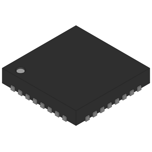
LTC2258-12 | 12-bit 65Msps ADC, CMOS Outputs, 5-170MHz, Requires DC890 and DC1075
Analog Devices Inc.DC1370A-J: Demo Board for the LTC2258-12 12-Bit, 65Msps Ultralow Power 1.8V ADCs
LTC2257-12 | 12-bit 40Msps ADC, CMOS Outputs, 5-170MHz, Requires DC890 and DC1075
Analog Devices Inc.DC1370A-K: Demo Board for the LTC2257-12 12-Bit, 40Msps Ultralow Power 1.8V ADCs

LTC2262-14 | 14-bit, 150Msps ADC, CMOS Outputs, 5-170MHz, Requires DC890 and DC1075
Analog Devices Inc.DC1370A-M: Demo Board for the LTC2262-14 14-Bit, 150Msps Ultralow Power 1.8V ADC

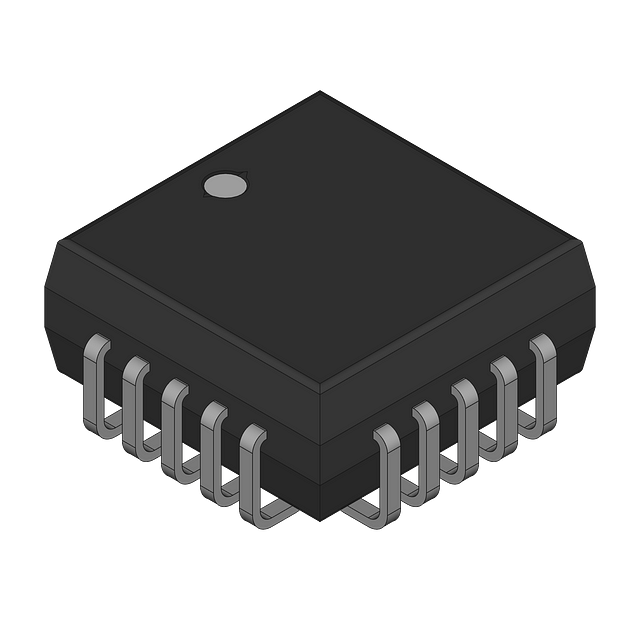
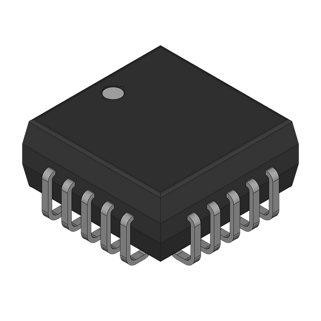
EVAL-AD5371EBZ
Analog Devices Inc.The AD5371 contains 40 14-bit DACs in a single 80-lead LQFP or 100-ball CSP_BGA. The device provides buffered voltage outputs with a span of 4? the reference voltage. The gain and…
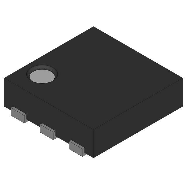

104130-HMC596LP4
Analog Devices Inc.The HMC596LP4(E) is a low-cost 4x2 switch matrix in a leadless QFN 4x4 mm surface mount package for use in Satellite/DBS, LNBs and multiswitches from 200 to 3000 MHz. A positive…

104356-HMC326MS8G
Analog Devices Inc.The HMC326MS8G & HMC326MS8GE are high efficiency GaAs InGaP Heterojunction Bipolar Transistor (HBT) MMIC driver amplifiers which operate between 3.0 and 4.5 GHz. The amplifier is…

105006-HMC414MS8G
Analog Devices Inc.The HMC414MS8G(E) is a high efficiency GaAs InGaP Heterojunction Bipolar Transistor (HBT) MMIC Power amplifier which operates between 2.2 and 2.8 GHz. The amplifier is packaged in…

105706-HMC385LP4
Analog Devices Inc.The HMC385LP4(E) is a GaAs InGaP Heterojunction Bipolar Transistor (HBT) MMIC VCO with integrated resonator, negative resistance device, varactor diode, and buffer amplifier.…

105706-HMC386LP4
Analog Devices Inc.The HMC386LP4(E) is a GaAs InGaP Heterojunction Bipolar Transistor (HBT) MMIC VCO with integrated resonator, negative resistance device, varactor diode, and buffer amplifiers.…

105786-HMC437MS8G
Analog Devices Inc.The HMC437MS8G(E) is a low noise Divide-by-3 Static Divider utilizing InGaP GaAs HBT technology in a low cost 8 lead surface mount plastic package. This device operates from DC…


