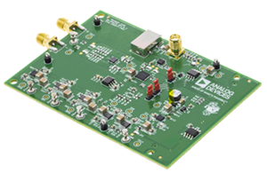
EV1HMC521ALC4
Analog Devices Inc.The HMC521ALC4 is a compact, gallium arsenide (GaAs), monolithic microwave integrated circuit (MMIC), inphase quadrature (I/Q) mixer in a RoHS compliant, 24-terminal ceramic leadless chip carrier (LCC) package. This device can be used as either an image reject mixer or a single sideband upconverter. The mixer uses two standard, double balanced mixer cells and a 90? hybrid coupler fabricated in a GaAs, metal?semiconductor field effect transistor (MESFET) process. This?device is a smaller alternative to hybrid style image reject?mixers and single sideband upconverter assemblies. The HMC521ALC4 eliminates the need for wire bonding, allowing?use of surface-mount manufacturing techniques.Applications Microwave and very small aperture terminal (VSAT) radios Test equipment Military electronic warfare (EW); electronic countermeasure (ECM); and command, control, communications, and intelligence (C3I)
EVAL-AD5141DBZ
Analog Devices Inc.The AD5121/AD5141 potentiometers provide a nonvolatilesolution for 128-/256-position adjustment applications, offeringguaranteed low resistor tolerance errors of ?8% and up to ?6 mAcurrent density in the A, B, and W pins.The low resistor tolerance and low nominal temperature coefficientsimplify open-loop applications as well as applications requiringtolerance matching.The linear gain setting mode allows independent programmingof the resistance between the digital potentiometer terminals,through RAW and RWB string resistors, allowing very accurateresistor matching.The high bandwidth and low total harmonic distortion (THD)ensure optimal performance for ac signals, making it suitablefor filter design.The low wiper resistance of only 40 ? at the ends of the resistorarray allows for pin-to-pin connection.The wiper values can be set through an SPI-/I2C-compatible digitalinterface that is also used to read back the wiper register andEEPROM contents.The AD5121/AD5141 is available in a compact, 16-lead, 3 mm ?3 mm LFCSP. The devices are guaranteed to operate over theextended industrial temperature range of ?40?C to +125?C.APPLICATIONS Portable electronics level adjustment LCD panel brightness and contrast controls Programmable filters, delays, and time constants Programmable power supplies
LT3570EUF Demo Board | Buck + Boost + LDO Controller, 4V to 36VIN Buck with VOUT1 = 3.3V@1A, 3.3V to 10VIN Boost with VOUT2 = 12V@275mA, 100mA LDO
Analog Devices Inc.Demonstration circuit 1106 is a 1.5A Buck Converter, 1.5A Boost Converter, and LDO Controller featuring the LT3570. The Buck is designed to convert a 4V to 36V source to 3.3V at 1A. The LDO is powered from the output of the buck and converts 3.3V to 2.5V at 100mA. The boost converts a 3.3V to 10V source to 12V at 275mA.
EV1HMC219BMS8G
Analog Devices Inc.The HMC219B is an ultraminiature, general-purpose, double balanced mixer in an 8-lead plastic surface mini small outline package with exposed pad (MINI_SO_EP). This passive monolithic microwave integrated circuit (MMIC) mixer is fabricated in a gallium arsenide (GaAs) metal semiconductor field effect transistor (MESFET) process and requires no external components or matching circuitry. The device can be used as an upconverter, downconverter, biphase demodulator, or phase comparator from 2.5 GHz to 7.0 GHz.The HMC219B provides excellent local oscillator (LO) to radio frequency (RF) isolation and LO to intermediate frequency (IF) isolation due to optimized balun structures. The RoHS compliant HMC219B eliminates the need for wire bonding and is compatible with high volume surface-mount manufacturing techniques. The consistent MMIC performance improves system operation and assures regulatory compliance with HiperLAN, U-NII, and ISM.Applications Microwave radios High performance radio local area network (HiperLAN) and unlicensed national information infrastructure (U-NII) Industrial, scientific, and medical (ISM)
AD8312-EVALZ
Analog Devices Inc.The AD8312 is a complete, low cost subsystem for the measurement of RF signals in the frequency range of 50 MHz to 3.5 GHz. It has a typical dynamic range of 45 dB and is intended for use in a wide variety of cellular handsets and other wireless devices. It provides a wider dynamic range and better accuracy than possible using discrete diode detectors. In particular, its temperature stability is excellent over the full operating range of ?40?C to +85?C.Its high sensitivity allows measurement at low power levels, thus reducing the amount of power that needs to be coupled to the detector. It is essentially a voltage-responding device, with a typical signal range of 1.25 mV to 224 mV rms or ?45 dBm to 0 dBm, referencing 50 ?.For convenience, the signal is internally ac-coupled, using a 5 pF capacitor to a load of 3 k? in shunt with 1.3 pF. This high-pass coupling, with a corner at approximately 16 MHz, determines the lowest operating frequency. Therefore, the source may be dc grounded.The AD8312 output, VOUT, increases from close to ground to about 1.2 V because the input signal level increases from 1.25 mV to 224 mV. A capacitor may be connected between the VOUT and CFLT pins when it is desirable to increase the time interval over which averaging of the input waveform occurs.The AD8312 is available in a 6-ball, 1.0 mm ? 1.5 mm, wafer-level chip scale package and consumes 4.2 mA from a 2.7 V to 5.5 V supply.Applications Cellular handsets (GSM, CDMA, WCDMA) RSSI and TSSI for wireless terminal devices Transmitter power measurement
LTC4370CDE Demo Board | Two-Supply Diode-OR Current Sharing Controller
Analog Devices Inc.DC1741B: Demo Board for the LTC4370 Two-Supply Diode-OR Current Balancing Controller.
LTC3728EG | Dual 2-Phase, 8V to 24V Input, 5V/3.3V 0A to 12A, 3.3V/2.5V 0A to 12A
Analog Devices Inc.Demonstration circuit 542 is a dual output, dual phase synchronous step-down controller, featuring the LTC3728EG. Output #1 can be configured for either 5.0V or 3.3V and output #2 can be configured for either 3.3V or 2.5V. The maximum load for both rails is 12A. The input voltage range of the DC542 is 8V to 24V. The DC542 also contains a footprint for a 5.5V boost converter bias supply whose output is connected to EXTVCC. See the “Optional Bias Supply” section for more details.
USB-I2C/LIN-CONV-Z
Analog Devices Inc.The ADuC7019?/?ADuC7020?/ ADuC7021 /?ADuC7022?/?ADuC7024?/?ADuC7025?/ ADuC7026?/?ADuC7027?/?ADuC7028?/?ADuC7029 are fully integrated,1 MSPS, 12-bit data acquisition systems incorporating highperformance multichannel ADCs, 16-bit/32-bit MCUs, andFlash?/EE memory on a single chip.The ADC consists of up to 12 single-ended inputs. An additionalfour inputs are available but are multiplexed with the four DACoutput pins. The four DAC outputs are available only on certainmodels (ADuC7020, ADuC7026, ADuC7028, and ADuC7029).However, in many cases where the DAC outputs are not present,these pins can still be used as additional ADC inputs, giving amaximum of 16 ADC input channels. The ADC can operate insingle-ended or differential input mode. The ADC input voltageis 0 V to VREF. A low drift band gap reference, temperature sensor,and voltage comparator complete the ADC peripheral set.Depending on the part model, up to four buffered voltageoutput DACs are available on-chip. The DAC output range isprogrammable to one of three voltage ranges.The devices operate from an on-chip oscillator and a PLLgenerating an internal high frequency clock of 41.78 MHz(UCLK). This clock is routed through a programmable clockdivider from which the MCU core clock operating frequencyis generated. The microcontroller core is an ARM7TDMI?,16-bit/32-bit RISC machine, which offers up to 41 MIPS peakperformance. Eight kilobytes of SRAM and 62 kilobytes ofnonvolatile Flash/EE memory are provided on-chip. TheARM7TDMI core views all memory and registers as a singlelinear array.On-chip factory firmware supports in-circuit serial downloadvia the UART or I2C serial interface port; nonintrusive emulationis also supported via the JTAG interface. These features areincorporated into a low cost QuickStart? development systemsupporting this MicroConverter? family.The parts operate from 2.7 V to 3.6 V and are specified over anindustrial temperature range of ?40?C to +125?C. Whenoperating at 41.78 MHz, the power dissipation is typically120 mW. The ADuC7019 / ADuC7020 / ADuC7021 /? ADuC7022 / ADuC7024 / ADuC7025 / ADuC7026 / ADuC7027 / ADuC7028 / ADuC7029 areavailable in a variety of memory models and packages (seeOrdering Guide).APPLICATIONS Industrial control and automation systems Smart sensors, precision instrumentation Base station systems, optical networking
DC2884A
Analog Devices Inc.The LTC3108 is a highly integrated DC/DC converter ideal for harvesting and managing surplus energy from extremely low input voltage sources such as TEGs (thermoelectric generators), thermopiles and small solar cells. The step-up topology operates from input voltages as low as 20mV. The LTC3108 is functionally equivalent to the LTC3108-1 except for its unique fixed VOUT options.Using a small step-up transformer, the LTC3108 provides a complete power management solution for wireless sensing and data acquisition. The 2.2V LDO powers an external microprocessor, while the main output is programmed to one of four fixed voltages to power a wireless transmitter or sensors. The power good indicator signals that the main output voltage is within regulation. A second output can be enabled by the host. A storage capacitor provides power when the input voltage source is unavailable. Extremely low quiescent current and high efficiency design ensure the fastest possible charge times of the output reservoir capacitor.The LTC3108 is available in a small, thermally enhanced 12-lead (3mm ? 4mm) DFN package and a 16-lead SSOP?package. Output Voltage (Switcher) LTC3108 Selectable 2.35V, 3.3V, 4.1V or 5V LTC3108-1 Selectable 2.5V, 3V, 3.7V or 4.5V Applications Remote Sensors and Radio Power Surplus Heat Energy Harvesting HVAC Systems Industrial Wireless Sensing Automatic Metering Building Automation Predictive Maintenance
EVAL-ADUC832QSZ
Analog Devices Inc.The ADuC832 is a complete, smart transducer front end, integrating a high performance self-calibrating multichannel 12-bit ADC, dual 12-bit DACs, and programmable 8-bit MCU on a single chip.The device operates from a 32 kHz crystal with an on-chip PLL, generating a high frequency clock of 16.78 MHz. This clock is, in turn, routed through a programmable clock divider from which the MCU core clock operating frequency is generated. The microcontroller core is an 8052 and is therefore 8051 instruction set compatible with 12 core clock periods per machine cycle. 62 kB of nonvolatile Flash/EE program memory are provided on chip. There are also 4 kB of nonvolatile Flash/EE data memory, 256 bytes of RAM, and 2 kB of extended RAM integrated on chip.The ADuC832 also incorporates additional analog functionality with two 12-bit DACs, a power supply monitor, and a band gap reference. On-chip digital peripherals include two 16-bit ?-? DACs, a dual-output 16-bit PWM, a watchdog timer, timeinterval counter, three timers/counters, Timer 3 for baud rate generation, and serial I/O ports (SPI, I2C?, and UART).Applications Optical networking?laser power control Base station systems Precision instrumentation, smart sensors Transient capture systems DAS and communications systems Upgrade to ADuC812 systems; runs from 32 kHz External crystal with on-chip PLL. Also available: ADuC831 pin-compatible upgrade to existing ADuC812 systems that require additional code or data memory; runs from 1 MHz to 16 MHz External crystal?
LTC2333-18 Demo Board | Buffered Octal, 18-Bit, 800Ksps Mux'd SAR ADC (Requires DC590, DC2026 or DC890)
Analog Devices Inc.Demonstration circuit 2365A highlights the LTC2358 family of buffered input ADCs. The LTC2358/LTC2357/LTC2353/LTC2333 are low noise, high speed, 16-/18-bit successive approximation register (SAR) ADCs with integrated front end buffers. These ADCs accept a wide common mode range. Pico-amp inputs and high CMRR enable these ADCs to connect directly to a wide range of sensors without compromising measurement accuracy. The demo manual refers to the LTC2358-18 but applies to all parts in the family, the only differences being the number of bits, number of channels and the maximum sample rate. The LTC2358-18 has a flexible SoftSpan™ interface that allows conversion-by-conversion control of the input voltage span on a per-channel basis. An internal 2.048V reference and 2X buffer simplify basic operation while an external reference can be used to increase the input range and the SNR of the ADC.
EV-ADUCRF101QSP3Z
Analog Devices Inc.The ADuCRF101 is a fully integrated, data acquisition solution that is designed for low power, wireless applications. It features a 12-bit analog-to-digital converter (ADC), a low power ARM Cortex?-M3 processor, a 862 MHz to 928 MHz and 431 MHz to 464 MHz RF transceiver, and Flash?/EE memory. The ADuCRF101 is packaged in a 9 mm ? 9 mm LFCSP.The data acquisition section consists of a 12-bit SAR ADC. The six inputs can be configured in single-ended or differential mode. When configured in single-ended mode, they can be used for ratiometric measurements on sensors that are powered, when required, from the internal low dropout regulator (LDO). An internal battery monitor channel and an on-chip temperature sensor are also available.This wireless data acquisition system is designed to operate in battery-powered applications where low power is critical. The device can be configured in normal operating mode or different low power modes under direct program control. In flexi mode, any peripheral can wake up the device and operate it. In hibernate mode, the internal wake-up timer remains active. In shutdown mode, only an external interrupt can wake up the device.The ADuCRF101 integrates a low power ARM Cortex-M3 processor. It is a 32-bit RISC machine, offering up to 1.25 DMIPS peak performance. The ARM Cortex-M3 processor also has a flexible 14-channel direct memory access (DMA) controller that supports communication peripherals, serial peripheral interface (SPI), UART, and I2C. Also provided on chip are 128 kB of nonvolatile Flash/EE memory and 16 kB of SRAM.A 16 MHz on-chip oscillator generates the system clock. This clock can be internally divided for the processor to operate at a lower frequency, thus saving power. A low power, internal 32 kHz oscillator is available and can be used to clock the four timers, as follows: two general-purpose timers, a wake-up timer, and a system watchdog timer.A range of communication peripherals can be configured, as required, in a specific application. These peripherals include UART, I2C, SPI, GPIO ports, PWM, and RF transceivers.The RF transceiver communicates in the 862 MHz to 928 MHz and 431 MHz to 464 MHz frequency bands using multiple configurations.On-chip factory firmware supports in-circuit serial download via the UART, and nonintrusive emulation and program download are also supported via the serial wire interface. These features are incorporated into a low cost development system supporting this precision analog microcontroller family.The ADuCRF101 operates from 2.2 V to 3.6 V and is specified over an industrial temperature range of ?40?C to +85?C. It is available in a 64-lead LFCSP packageApplications Battery powered wireless sensor Medical telemetry systems Industrial and home automation Asset tracking Security systems (access systems) Health and fitness applications??
EVAL-AD5243SDZ
Analog Devices Inc.The AD5243 and AD5248 provide a compact 3 mm ? 4.9 mmpackaged solution for dual, 256-position adjustment applications.The AD5243 performs the same electronic adjustment functionas a 3-terminal mechanical potentiometer, and the AD5248performs the same adjustment function as a 2-terminal variableresistor. Available in four end-to-end resistance values (2.5 k?,10 k?, 50 k?, and 100 k?), these low temperature coefficientdevices are ideal for high accuracy and stability-variableresistance adjustments. The wiper settings are controllablethrough the I2C-compatible digital interface. The AD5248 hasextra package address decode pins, AD0 and AD1, allowingmultiple parts to share the same I2C, 2-wire bus on a PCB. Theresistance between the wiper and either endpoint of the fixedresistor varies linearly with respect to the digital code transferred into the RDAC latch. (The terms digital potentiometer, VR,and RDAC are used interchangeably.)Operating from a 2.7 V to 5.5 V power supply and consumingless than 6 ?A allows the AD5243/AD5248 to be used inportable battery-operated applications.For applications that program the AD5243/AD5248 at thefactory, Analog Devices, Inc., offers device programmingsoftware running on Windows? NT/2000/XP operating systems.This software effectively replaces the need for external I2Ccontrollers, which in turn enhances the time to market ofsystems. An AD5243/AD5248 evaluation kit and software areavailable. The kit includes a cable and instruction manual.Applications Systems calibrations Electronics level settings Mechanical trimmers replacement in new designs Permanent factory printed circuit board (PCB) setting Transducer adjustment of pressure, temperature, position, chemical, and optical sensors RF amplifier biasing Gain control and offset adjustment
EVAL-AD7091R-4SDZ
Analog Devices Inc.The AD7091R-2/AD7091R-4/AD7091R-8 family is a multichannel12-bit, ultralow power, successive approximation analog-to-digitalconverter (ADC) that is available in two, four, or eightanalog input channel options. The AD7091R-2/AD7091R-4/AD7091R-8 operate from a single 2.7 V to 5.25 V power supplyand are capable of achieving a sampling rate of 1 MSPS.The AD7091R-2/AD7091R-4/AD7091R-8 family offers up to eightsingle-ended analog input channels with a channel sequencerthat allows a preprogrammed selection of channels to be convertedsequentially. The AD7091R-2/AD7091R-4/ AD7091R-8 alsofeature an on-chip conversion clock, an on-chip accurate 2.5 Vreference, and a high speed serial interface.The AD7091R-2/AD7091R-4/AD7091R-8 have a serial portinterface (SPI) that allows data to be read after the conversionwhile achieving a 1 MSPS throughput rate. The conversion processand data acquisition are controlled using the CONVST pin.The AD7091R-2/AD7091R-4/AD7091R-8 use advanced designtechniques to achieve ultralow power dissipation at highthroughput rates. They also feature flexible power managementoptions. An on-chip configuration register allows the user to set updifferent operating conditions. These include power management,alert functionality, busy indication, channel sequencing, andgeneral-purpose output pins. The MUXOUT and ADCIN pinsallow signal conditioning of the multiplexer output prior toacquisition by the ADC.APPLICATIONS Battery powered systems Personal digital assistants Medical instruments Mobile communications Instrumentation and control systems Data acquisition systems Optical sensors Diagnostic/monitoring functions
LTC4061EDD | Single Cell Li-Ion Battery Charger, VIN = 4.3V to 8V, Batt = 4.2V @ 50mA to 1A
Analog Devices Inc.Demonstration circuit 788A is a complete constant-current, constant-voltage battery charger for one Lithium-Ion cell and featuring the LTC4061EDD. The demo board has an input voltage range of 4.3V to 8V, suitable for USB applications. Jumpers on the board allow charge currents from 50mA to 1A to be programmed and several charge termination methods to be used. Terminals are provided for adding a thermistor for sensing battery temperature, shutting down the charger, monitoring charge current and programming the minimum charge current level for termination (IDETECT).
The LTC4061 features an internal P-channel power MOSFET with a unique thermal feedback loop that reduces the output current under high ambient temperature and/or high power dissipation conditions. This feature allows the charger to provide higher charge currents under normal conditions and still provide safe charging under abnormal conditions such as high ambient temperature, high input voltage or low battery voltage.
LT3080EDD-1 Demo Board | LT3080-1(x4), Paralleled, Single Resistor Prog Low Noise LDOs, 1.7V ≤ VIN ≤ 25V, VOUT = 1.2V @ 4.4A
Analog Devices Inc.Demonstration circuit 1368A exercises four adjustable linear regulators in parallel using the LT3080-1, which incorporates an internal ballast resistor. The ballast resistor allows direct paralleling of devices without the need for PC board resistors or sensor resistors.The paralleled devices provide up to 4.4A of output current at 1.2V.
Architected as a precision current source and voltage follower, the LT3080-1 can be used in many applications requiring high current, adjustability to zero output, and no heat sink. The device brings out the collector of the pass transistor to allow low dropout operation when used with multiple supplies. The LT3080-1's output voltage can be programmed to any level between 0V and 36V; however the demo board has a reduced input voltage range from 1.7V to 25V due to the input capacitor voltage rating.
EV1HMC6789BLC5A
Analog Devices Inc.The HMC6789BLC5A is a compact GaAs MMIC I/Qdownconverter in a 12-terminal, RoHS compliant,ceramic leadless chip carrier (LCC) package. Thisdevice provides a small signal conversion gain of 14 dBwith 25 dBc of image rejection. The HMC6789BLC5Autilizes a low noise amplifier to drive the I/Q mixerwhere the LO is driven by a ?2 multiplier. IF1 and IF2mixer inputs are provided and an external 90? hybridis needed to select the required sideband. The I/Qmixer topology reduces the need for filtering of theunwanted sideband. The HMC6789BLC5A is a muchsmaller alternative to hybrid style single sidebanddownconverter assemblies and it eliminates the needfor wire bonding by allowing the use of surface mountmanufacturing techniques.Applications Point-to-Point and Point-to-Multi-Point Radios Military Radar, EW & ELINT Satellite Communications Sensors
DC1988A
Analog Devices Inc.The LTM8058 is a 2kV AC isolated flyback ?Module? (power module) DC/DC converter with LDO post regulator. Included in the package are the switching controller, power switches, transformer, LDO, and all support components. Operating over an input voltage range of 3.1V to 31V, the LTM8058 supports an output voltage range of 2.5V to 13V, set by a single resistor. There is also a linear post regulator whose output voltage is adjustable from 1.2V to 12V as set by a single resistor. Only output and input capacitors are needed to finish the design. Other components may be used to control the soft-start control and biasing.The LTM8058 is packaged in a thermally enhanced, compact (9mm ? 11.25mm ? 4.92mm) overmolded ball grid array (BGA) package suitable for automated assembly by standard surface mount equipment. The LTM8058 is available with SnPb or RoHS compliant terminal finish.Applications Industrial Sensors Industrial Switches Ground Loop Mitigation
AD9554/PCBZ
Analog Devices Inc.The AD9554 is a low loop bandwidth clock translator that provides jitter cleanup and synchronization for many systems, including synchronous optical networks (SONET/SDH). The AD9554 generates an output clock synchronized to up to four external input references. The digital PLL (DPLL) allows for reduction of input time jitter or phase noise associated with the external references. The digitally controlled loop and holdover circuitry of the AD9554 continuously generates a low jitteroutput clock even when all reference inputs have failed.The AD9554 operates over an industrial temperature range of ?40?C to +85?C. If a smaller device is needed, the AD9554-1 is a version of this device with one output per PLL. If a single or dual DPLL version of this device is needed, refer to the AD9557 or AD9559, respectively.Applications Network synchronization, including synchronous Ethernet and synchronous digital hierarchy (SDH) to optical transport network (OTN) mapping/demapping Cleanup of reference clock jitter SONET/SDH clocks up to OC-192, including FEC Stratum 3 holdover, jitter cleanup, and phase transient control Cable infrastructure Data communications Professional video
EVAL-ADV8005-SMZ
Analog Devices Inc.The ADV8005 is a multiple input video signal processor that can deinterlace and scale standard definition (SD), enhanced definition (ED), or high definition (HD) video data to ultra HD formats; generate a bitmap on-screen display (OSD); and output the video with OSD overlaid on two High-Definition Multimedia Interface (HDMI?) transmitters and a video encoder.The 60-bit TTL video port can be used to input video to the ADV8005 in a number of ways: using the 48-bit TTL pixel port, using the 24-bit external OSD TTL pixel port, or from a device with an HDMI transmitter such as the ADV7850. The ADV8005 supports many of the formats outlined in the CEA-861-F and VESA specifications, as well as several other widely used timing formats.The ADV8005 features primary and secondary video scalers that enable simultaneous output of multiple different resolutions. The primary video scaler can upscale to 4k ? 2k modes. The secondary video scaler can upscale to 1080p or UXGA graphics. 4k ? 2k downscaling is performed using the secondary video scaler, leaving the primary video scaler available for other video processing.The ADV8005 primary video scaler can perform high performance, motion adaptive interlaced to progressive conversion on SD and HD content. Additional functionality has also been added to ADV8005 to facilitate upscaling and downscaling to VESA formats with pixel clock frequencies below 300 MHz.Detail enhancement and image enhancing techniques such as random, mosquito, and block noise reduction allow improved final image quality. The frame rate converter of the ADV8005 allows the conversion between common frame rates with support to output two different frame rates simultaneously under certain conditions. The VSP can do aspect ratio conversion, CUE correction, crop output image.The ADV8005 can accept OSD video from an external OSD source on one of its inputs and it can internally generate a high quality, bitmap-based OSD. The internal OSD is highly flexible and allows the system designer to easily incorporate features like scrolling text and animation in various color depths up to 24-bit true color with alpha blending, such as RGB565, ARGB4444 and ARGB8888.Analog Devices, Inc., provides an OSD development tool (Blimp) to assist in the design, debug, and emulation of the OSD prior to integration with the system application. When the design is complete, the OSD development tool automatically generates code to which system application programming interfaces (APIs) can be added before integration with the system application and an OSD design resource, which must be downloaded to an external SPI flash memory.Video can be output from the ADV8005 using one or both of the HDMI transmitters and/or the six-DAC SD/HD video encoder. The six 12-bit NSV? video DACs allow composite (CVBS), S-Video (Y/C), and component (YPrPb) analog outputs in standard, enhanced, and high definition video formats. Oversampling of 216 MHz (SD and ED) and 297 MHz (HD) removes the requirement for external output filtering. Rovi? and non-Rovi variants of the ADV8005 are available.Both of the HDMI transmitters on the ADV8005 support 4k ? 2k and all mandatory and many optional 3D video resolutions. Each transmitter features an audio return channel receiver (ARC). The ADV8005 can receive up to eight channels of I2S, S/PDIF, direct stream digital (DSD), and high bit rate (HBR) audio passed from either the serial video Rx or from the externally available audio input pins.The ADV8005 supports the I2C protocol for communication with the system microcontroller. APPLICATIONS High end A/V receivers Upconverting DVD players/recorders Video conferencing and distribution HDMI splitters Video walls 4k HDMI transmitter


