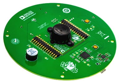
EVAL-AD5142ADBZ
Analog Devices Inc.The AD5122A/AD5142A potentiometers provide a nonvolatile solution for 128-/256-position adjustment applications, offering guaranteed low resistor tolerance errors of ?8% and up to ?6 mA current density in the Ax, Bx, and Wx pins.The low resistor tolerance and low nominal temperature coefficient simplify open-loop applications as well as applications requiring tolerance matching.The linear gain setting mode allows independent programming of the resistance between the digital potentiometer terminals, through RAW and RWB the string resistors, allowing very accurate resistor matching.The high bandwidth and low total harmonic distortion (THD) ensure optimal performance for ac signals, making it suitable for filter design.The low wiper resistance of only 40 ? at the ends of the resistor array allows for pin-to-pin connection.The wiper values can be set through an I2C-compatible digital interface that is also used to read back the wiper register and EEPROM contents.The AD5122A/AD5142A are available in a compact, 16-lead, 3 mm ? 3 mm LFCSP and a 16-lead TSSOP. The parts are guaranteed to operate over the extended industrial temperature range of ?40?C to +125?C.APPLICATIONS Portable electronics level adjustment LCD panel brightness and contrast controls Programmable filters, delays, time constants Programmable power supplies
LTC4150CMS | Coulomb Counter/Battery Gas Gauge (requires DC590 Controller)
Analog Devices Inc.DC756A: Demo Board for the LTC4150 Coulomb Counter/Battery Gas Gauge.
ADCLK944/PCBZ
Analog Devices Inc.The ADCLK944 is an ultrafast clock fanout buffer fabricated on the Analog Devices, Inc., proprietary XFCB3 silicon germanium (SiGe) bipolar process. This device is designed for high speed applications requiring low jitter.The device has a differential input equipped with center-tapped, differential, 100 ? on-chip termination resistors. The input can accept dc-coupled LVPECL, CML, 3.3 V CMOS (single-ended), and ac-coupled 1.8 V CMOS, LVDS, and LVPECL inputs. A VREF pin is available for biasing ac-coupled inputs.The ADCLK944 features four full-swing emitter-coupled logic (ECL) output drivers. For LVPECL (positive ECL) operation, bias VCC to the positive supply and VEE to ground. For ECL operation, bias VCC to ground and VEE to the negative supply.The ECL output stages are designed to directly drive 800 mV each side into 50 ? terminated to VCC ? 2 V for a total differential output swing of 1.6 V.The ADCLK944 is available in a 16-lead LFCSP and is specified for operation over the standard industrial temperature range of ?40?C to +85?C.?APPLICATIONS Low jitter clock distribution Clock and data signal restoration Level translation Wireless communications Wired communications Medical and industrial imaging ATE and high performance instrumentation
DC2769A-A-KIT
Analog Devices Inc.The LTC4124 is a simple high performance wireless Li-Ion charger with low battery disconnect. The pin-selectable charge current (up to 100mA) and charge voltage ensure versatility while minimizing the number of required external components.Wireless charging with the LTC4124 allows devices to be charged while sealed within enclosures and eliminates bulky connectors in space-constrained applications. Elimination of exposed conductive connectors also creates more robust devices while ensuring an effortless end-user experience.The LTC4124 includes an NTC input for safe temperature qualified charging and a battery disconnect feature that prevents damage to a battery due to over-discharging.The 2mm ? 2mm LQFN package and minimal number of external components make the LTC4124 well-suited for low power portable applications where small solution size is mandatory.Applications Medical Wireless Sensors Military Wearables High End Wireless Headsets Streaming Headsets with Bluetooth Connectivity Virtual Reality Headsets High End Remote Control IoT Devices
AD9553/PCBZ
Analog Devices Inc.The AD9553 is a phase-locked loop (PLL) based clock translator designed to address the needs of passive optical networks (PON) and base stations. The device employs an integer-N PLL to accommodate the applicable frequency translation requirements. The user supplies up to two single-ended input reference signals or one differential input reference signal via the REFA and REFB inputs. The device supports holdover applications by allowing the user to connect a 25 MHz crystal resonator to the XTAL input.The AD9553 is pin programmable, providing a matrix of standard input/output frequency translations from a list of 15 possible input frequencies to a list of 52 possible output frequency pairs (OUT1 and OUT2). The device also has a 3-wire SPI interface, enabling the user to program custom input-to-output frequency translations.The AD9553 output is compatible with LVPECL, LVDS, or single-ended CMOS logic levels, although the AD9553 is implemented in a strictly CMOS process.The AD9553 operates over the extended industrial temperature range of ?40?C to +85?C.APPLICATIONS Cost effective replacement of high frequency VCXO, OCXO, and SAW resonators Extremely flexible frequency translation for SONET/SDH, Ethernet, Fibre Channel, DRFI/DOCSIS, and PON/EPON/GPON Wireless infrastructure Test and measurement (including handheld devices)
EVAL-ADXL355Z
Analog Devices Inc.The analog output ADXL354 and the digital output ADXL355 are low noise density, low 0 g offset drift, low power, 3-axis accelerometers with selectable measurement ranges. The ADXL354B supports the ?2 g and ?4 g ranges, the ADXL354C supports the ?2 g and ?8 g ranges, and the ADXL355 supports the ?2 g, ?4 g, and ?8 g ranges. The ADXL354/ADXL355 offerindustry leading noise, minimal offset drift over temperature, and long-term stability enabling precision applications with minimal calibration.Highly integrated in a compact form factor, the low power ADXL355 is ideal in an Internet of Things (IoT) sensor node and other wireless product designs. The ADXL355 multifunction pin names may be referenced by their relevant function only for either the serial peripheral interface (SPI) or I2C interface.Applications Inertial measurement units (IMUs)/altitude and heading reference systems (AHRS) Platform stabilization systems Structural health monitoring Seismic imaging Tilt sensing Robotics Condition Monitoring
114399-HMC542BLP4
Analog Devices Inc.The HMC542BLP4E is a broadband 6-bit GaAs IC digital attenuator with a CMOS compatible serial to parallel driver in low cost leadless surface mount package. This serial control digital attenuator incorporates off chip AC ground capacitors for near DC operation, making it suitable for a wide variety of RF and IF applications. Covering DC to 4 GHz, the insertion loss is 1.7 dB and the attenuator bit values are 0.5 (LSB), 1, 2, 4, 8, and 16 dB for a total attenuation of 31.5 dB. Attenuation accuracy is excellent at ?0.25 dB typical step error with an IIP3 of +50 dBm. Six bit serial control words are used to select each attenuation state. A single VCC bias of +5V is required.APPLICATIONS Cellular/PCS/3G Infrastructure ISM, MMDS, WLAN, WiMAX, & WiBro Microwave Radio & VSAT Test Equipment and Sensors
DC2373A
Analog Devices Inc.The LT8641 step-down regulator features Silent Switcher architecture designed to minimize EMI/EMC emissions while delivering high efficiency at frequencies up to 3MHz. Assembled in a 3mm ? 4mm QFN, the monolithic construction with integrated power switches and inclusion of all necessary circuitry yields a solution with a minimal PCB footprint. An ultralow 2.5?A quiescent current?with the output in full regulation?enables applications requiring highest efficiency at very small load currents. Transient response remains excellent and output voltage ripple is below 10mVP-P at any load, from zero to full current.The LT8641 allows high VIN to low VOUT conversion at high frequency with a fast minimum top switch on-time of 35ns. Operation is safe in overload even with a saturated inductor.Essential features are included and easy to use: An open-drain PG pin signals when the output is in regulation. The SYNC/MODE pin selects between Burst Mode, pulse-skipping, or spread spectrum mode, and also allows synchronization to an external clock. Soft-start and tracking functionality is accessed via the TR/SS pin. An accurate enable threshold can be set using the EN/UV pin and a resistor at the RT pin programs switch frequency.APPLICATIONS Automotive and Industrial Supplies General Purpose Step-Down GSM Power Supplies
LT8338 | 1.2A, 42V Micropower Synchronous Boost Converter
Analog Devices Inc.Demonstration circuit DC2907A features the LT8338, a low IQ, Synchronous Boost Converter in a thermally enhanced 10-lead plastic MSOP package. DC2907A is designed to convert a 4V to 16V source to 24V output, with up to 460mA of load current, depending on the input voltage. It was designed with a switching frequency of 2.2MHz.
DC2907A contains a selectable jumper, JP1, to aid in the selection of any of the five modes of operation. The default setting is Burst mode.
This converter features Spread Spectrum Frequency Modulation, SSFM. The input and output filters installed on the PCB help suppress EMI noise, but the use of SSFM makes it easier to pass CISPR25 class 5 conducted and radiated emissions testing for automotive vehicles. To perform an EMI evaluation for this converter include the input filter by connecting the input source to the VEMI terminal and select the Burst+SSFM JP1 setting.
EMI filters may not be necessary for all applications. For a lower parts count and BOM cost EMI filters can be removed. To do so, replace FB1 and FB2 with a zero ohm jumpers and remove all input and output filter components located inside the dashed-line rectangles on the schematic, plus C1 and C13.
Proper board layout is essential for maximum thermal performance. See the datasheet section “Thermal Considerations”.
The Performance Summary section details the ratings of the DC2907A at room temperature. The LT8338 datasheet gives a complete description of the part, operation and application information. The data sheet must be read in conjunction with this quick start guide for DC2907A.
The LT8338 is available in a thermally-enhanced 10 lead plastic MSOP package.
ADIS16505-2/PCBZ
Analog Devices Inc.The ADIS16505 is a precision, miniature microelectromechanical system (MEMS) inertial measurement unit (IMU) that includes a triaxial gyroscope and a triaxial accelerometer. Each inertial sensor in the ADIS16505 combines with signal conditioning that optimizes dynamic performance. The factory calibration characterizes each sensor for sensitivity, bias, alignment, linear acceleration (gyroscope bias), and point of percussion (accelerometer location). As a result, each sensor has dynamic compensation formulas that provide accurate sensor measurements over a broad set of conditions.The ADIS16505 provides a simplified, cost effective method for integrating accurate, multi-axis inertial sensing into industrial systems, especially when compared with the complexity and investment associated with discrete designs. All necessary motion testing and calibration are part of the production process at the factory, greatly reducing system integration time. Tight orthogonal alignment simplifies inertial frame alignment in navigation systems. The serial peripheral interface (SPI) and register structure provide a simple interface for data collection and configuration control.The ADIS16505 is available in a 100-ball, ball grid array (BGA) package that is approximately 15 mm ? 15 mm ? 5 mm.Applications Navigation, stabilization, and instrumentation Unmanned and autonomous vehicles Smart agriculture and construction machinery Factory/industrial automation, robotics Virtual/augmented reality Internet of Moving Things
ADIS16203/PCBZ
Analog Devices Inc.The ADIS16203 is a complete incline-angle measurement system ina single compact package enabled by the Analog Devices, Inc.,iSensor? integration. By enhancing the Analog Devices iMEMS?sensor technology with an embedded signal processing solution, the ADIS16203 provides factory-calibrated, sensor-to-digital incline-angle data in a convenient format that can be accessed using aserial peripheral interface (SPI). The SPI interface provides access to multiple measurements: 360? linear inclination angles, ?180?linear incline angles, temperature, power supply, and one auxiliaryanalog input. Easy access to calibrated digital sensor data providesdevelopers with a system-ready device, reducing developmenttime, cost, and program risk.Unique characteristics of the end system are accommodatedeasily through several built-in features, such as a single-command offset calibration, along with convenient sample rate and band-width control.The ADIS16203 offers the following embedded features that eliminate the need for external circuitry and provide a simplified system interface: Configurable alarm function Auxiliary 12-bit analog-to-digital converter (ADC) Auxiliary 12-bit digital-to-analog converter (DAC) Configurable digital I/O port Digital self-test functionThe ADIS16203 offers two power management features formanaging system-level power dissipation: low power mode anda configurable shutdown feature.The ADIS16203 is available in a 9.2 mm ? 9.2 mm ? 3.9 mmlaminate-based land grid array (LGA) package with a temperature range of ?40?C to +125?C.APPLICATIONS Tilt sensing, inclinometers Platform control, stabilization, and leveling Motion/position measurement Monitor/alarm devices (security, medical, safety) Robotics
LTC4281 Demo Board | 12V, 50A Hot Swap Controller with Telemetry [Requires DC1613]
Analog Devices Inc.Demonstration circuit 2278A features the LTC4281 hot swap controller. The LTC4281 is well suited to high power applications because the precise monitoring capability and accurate current limiting reduces the extremes in which both loads and power supplies must safely operate. Non-volatile configuration allows for flexibility in the autonomous generation of alerts and response to faults.
EVAL-ADAU1850EBZ
Analog Devices Inc.The ADAU1850 is a codec with three inputs and one output that incorporates one digital signal processor. The path from the analog input to the DSP core to the analog output is optimized for low latency and is ideal for noise canceling earphones. With the addition of a few passive components, the ADAU1850 provides a complete headset solution.The ADAU1850 is provided in a small, 28-ball, 2.957 mm ? 1.757 mm wafer level chip scale package (WLCSP).APPLICATIONS Noise canceling handsets, headsets, and headphones Bluetooth active noise canceling (ANC) handsets, headsets, and headphones Personal navigation devices Digital still and video cameras Musical instrument effect processors Multimedia speaker systems Smartphones
DC1016A-A
Analog Devices Inc.The LT6557 is a high speed triple video ampli?er with an internal ?xed gain of 2 and a programmable DC input bias voltage. This ampli?er features a 400MHz 2VP-P signal bandwidth, 2200V/?s slew rate and a unique ability to drive heavy output loads to 0.8V of the supply rails, making the LT6557 ideal for a single 5V supply, wideband video application. With just one resistor, the inputs of all three ampli?ers can be programmed to a common voltage level, simplifying and reducing the need for external circuitry in the AC-coupled applications. Without the programmable resistor, the input bias circuit becomes inactive, allowing the use of an external clamp circuit or direct coupled input.The LT6557 has separate power supply and ground pins for each ampli?er to improve channel separation and to ease power supply bypassing. The LT6557 provides uncompromised performance in many high speed applications where a low voltage, single supply is required.The LT6557 is available in 16-lead SSOP and 5mm ? 3mm DFN packages.Applications LCD Video Projectors RGB HD Video Ampli?ers Coaxial Cable Drivers Low Supply ADC Drivers
DC2914A-B
Analog Devices Inc.The LTC4238 is a high voltage high current Hot Swap controller that allows a board to be safely inserted and removed from a live backplane. Dual 12V gate drive is well suited for high power applications to either share safe operating area across parallel MOSFETs or support a 2-stage start-up that first charges the load capacitance followed by enabling a low on-resistance path to the load.The device features active current limiting (ACL) with two foldback options as VDS increases. The constant power profile limits the power dissipation to be no higher than a fixed value, while the high power profile allows the part to ride through large input steps during operation.The LTC4238 notifies when output power is good. In addition, it has protection features that respond to input undervoltage, overvoltage; and generate a fault when there is an overcurrent or FET bad condition.Applications Live Board Insertion in 12V, 24V and 48V Systems Industrial High Side Switch/Circuit Breaker Computers, Servers Vehicle Electrical Systems
LTC3308A Demo Board | 5V Input to 1.2V Output at 4A Synchronous Step‑Down Silent Switcher Demo Circuit
Analog Devices Inc.Demonstration circuit 2991A features the LTC3308A 5V, 4A synchronous step-down Silent Switcher® operating as a 2.0MHz, 3.3V to 1.2V 4A buck regulator. The LTC3308A supports adjustable output voltages from 0.5V to VIN with operating frequencies from 1MHz up to 3MHz. The LTC3308A is a compact, ultralow emission, high efficiency, and high speed synchronous monolithic stepdown switching regulator. A minimum on-time switching of 22ns enables high VIN to low VOUT conversion ratios at high frequencies.
The DC2991A operating mode may be selected as BURST, SKIP or Forced Continuous (FC) mode. Setting JP1 to the FC/SYNC position will allow the LTC3308A to sync to a clock frequency from 1MHz to 3MHz. The LTC3308A operates in forced continuous mode when syncing to an external clock. The DC2991A is set to a fixed 2MHz frequency by connecting RT to VIN through a 0Ω resistor, R9. The frequency can be easily changed by removing R9 and setting an appropriate resistor in the R4 location to obtain the desired frequency. Refer to the LTC3308A data sheet for the proper RT value for a desired switching frequency.
The DC2991A also has an EMI filter to reduce conducted EMI. This EMI filter can be included by applying the input voltage at the VIN EMI terminal. The EMI performance of the board is shown in the EMI Test Results section. The red lines in the EMI performance graphs illustrate the CISPR25 Class 5 peak limits for the conducted and radiated emission tests.
The LTC3308A data sheet gives a complete description of the device, operation and application information. The data sheet must be read in conjunction with this demo manual. The LTC3308A is assembled in a 2mm × 2mm LQFN package with exposed pads for low thermal resistance. The layout recommendations for low EMI operation and maximum thermal performance are available in the data sheet section: Low EMI PCB Layout.
The Efficiency vs Load graph shows the efficiency and the power loss of the circuit with a 3.3V input in Burst Mode operation.
LTC3780EG/LTC4440ES6 Demo Board | Buck-Boost, VIN: 36V to 72V, VOUT 48V/5A
Analog Devices Inc.Demonstration circuit 1046A is a non-isolated, high efficiency buck-boost DC/DC supply featuring LTC3780EG and LTC4440ES6. The LTC3780 is a high performance 4-switch synchronous buck boost regulator and the LTC4440 is a 100V-rated FET driver. The input voltage of the demo board is designed for 36V to 72V. The output voltage is 48V. At 25C° room temperature, the maximum output current is 5A without a cooling fan and 6A with 150LFM air flow for cooling. An optional 12V bias flyback supply using the LTC3803 is stuffed on the board to power the LTC3780 and LTC4440.
DC1028A
Analog Devices Inc.The LT3513 5-output adjustable switching regulator provides power for large TFT-LCD panels. The 38-pin 5mm ? 7mm QFN device can generate a 3.3V or 5V logic supply along with the triple output supply required for the TFT-LCD panel. A lower voltage secondary logic supply may also be generated with the addition of an external NPN driven by the internal linear regulator. A step-down regulator provides a low voltage output, VLOGIC, with up to 1.2A of current while capable of operating from a wide input range of 4.5V to 30V. A high power step-up converter, a lower power step-up converter and an inverting converter provide the three independent output voltages: AVDD, VON and VOFF required by the LCD panel. A high-side PNP provides delayed turn-on of the VON signal and can handle up to 30mA. Protection circuitry ensures that VON is disabled if any of the four outputs are more than 10% below the programmed voltage.Applications Automotive TFT-LCD Displays Large TFT-LCD Desktop Monitors Flat Panel Televisions
EV1HMC525ALC4
Analog Devices Inc.The HMC525ALC4 is a compact gallium arsenide (GaAs), monolithic microwave integrated circuit (MMIC), in phase quadrature (I/Q) mixer in a 24-terminal, RoHS compliant, ceramic leadless chip carrier (LCC) package. The device can be used as either an image reject mixer or a single sideband (SSB) upconverter. The mixer uses two standard double balanced mixer cells and a 90? hybrid fabricated in a GaAs, metalsemiconductor field effect transistor (MESFET) process. The HMC525ALC4 is a much smaller alternative to a hybrid style image reject mixer and a SSB upconverter assembly. The HMC525ALC4 eliminates the need for wire bonding, allowing the use of surface-mount manufacturing techniques. Applications Microwave and very small aperture terminal radios Test equipment Point to point radios Military electronic warfare; electronic countermeasure; and command, control, communications, and intelligence
LT3760 Demo Board | 8-Channel Boost LED Driver, 20V ≤ VIN ≤ 28V, VLED = 55V @ 100mA
Analog Devices Inc.DC1573A is an 8-Channel High Voltage Boost LED Driver featuring the LT3760. The LT3760 drives up to 100mA per string and has a maximum LED string voltage of 45V. The VIN terminal is powered from an 10V to 14V input supply and is distinct from the 24V PVIN supply (20V to 28V) for best thermal performance. Overvoltage protection is set at 55V in case the LEDs are removed from the circuit. If the LEDs are opened, the FAULT terminal output flag goes low and reports the fault condition. If one or more of the 8 LED channels is not used, its LED pin or terminal should be tied to VOUT (LED+) to disable it. Multiple channels can be tied in parallel by tying their LED1-LED8 pins together.


