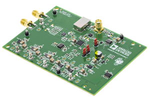
AD9176-FMC-EBZ
Analog Devices Inc.The AD9176 is a high performance, dual, 16-bit digital-to-analog converter (DAC) that supports DAC sample rates up to 12.6 GSPS. The device features an 8-lane, 15.4 Gbps JESD204B data input port, a high performance, on-chip DAC clock multiplier, and digital signal processing capabilities targeted at single-band and multiband direct to radio frequency (RF) wireless applications.The AD9176 features three complex data input channels per RF DAC datapath. Each input channel is fully bypassable. Each data input channel (or channelizer) includes a configurable gain stage, an interpolation filter, and a channel numerically controlled oscillator (NCO) for flexible, multiband frequency planning. The AD9176 supports an input data rate of up to a 3.08 GSPS complex (inphase/quadrature (I/Q)), or up to 6.16 GSPS non-complex (real), and is capable of allocating multiple complex input data streams to the assigned channels for individual processing. Each group of three channelizers is summed into a respective main datapath for additional processing when needed. Each main datapath includes an interpolation filter and one 48-bit main NCO ahead of the RF DAC core. Using the modulator switch, the outputs of a main datapath can be either routed to DAC0 alone for operating as a single DAC, or routed to both DAC0 and DAC1 for operating as a dual, intermediate frequency DAC (IF DAC).The AD9176 also supports ultrawide data rate modes that allow bypassing the channelizers and main datapaths to provide maximum data rates of up to 6.16 GSPS as a single, 16-bit DAC, up to 3.08 GSPS as a dual, 16-bit DAC, or up to 4.1 GSPS as a dual, 12-bit DAC.The AD9176 is available in a 144-ball BGA_ED package.Applications Wireless communications infrastructure Multiband base station radios Microwave/E-band backhaul systems Instrumentation, automatic test equipment (ATE) Radars and jammersProduct Highlights A low power, multichannel, dual DAC design reduces power consumption in higher bandwidth and multichannel applications, while maintaining performance. Supports single-band and multiband wireless applications with three bypassable complex data channels per RF DAC, or configurations that use the two main datapaths as two wideband complex data channels when using the built in modulator switch. A maximum complex data rate (per I or Q) of up to 3.08 GSPS with 16-bit resolution, and up to 4.1 GSPS with 12-bit resolution. The AD9176 can be alternatively configured as a dual DAC, with each DAC operating across an independent JESD204B link, at the previously described data rates. Ultrawide bandwidth single-DAC modes, supporting up to 6.16 GSPS data rates with 16-bit resolution.
AD9204-20EBZ
Analog Devices Inc.The AD9204 is a monolithic, dual-channel, 1.8 V supply, 10-bit, 20 MSPS/40 MSPS/65 MSPS/80 MSPS analog-to-digital converter (ADC). It features a high performance sample-and-hold circuit and on-chip voltage reference.The product uses multistage differential pipeline architecture with output error correction logic to provide 10-bit accuracy at 80 MSPS data rates and to guarantee no missing codes over the full operating temperature range.The ADC contains several features designed to maximize flexibility and minimize system cost, such as programmable clock and data alignment and programmable digital test pattern generation. The available digital test patterns include built-in deterministic and pseudorandom patterns, along with custom user-defined test patterns entered via the serial port interface (SPI).A differential clock input controls all internal conversion cycles. An optional duty cycle stabilizer (DCS) compensates for wide variations in the clock duty cycle while maintaining excellent overall ADC performance.The digital output data is presented in offset binary, gray code, or twos complement format. A data output clock (DCO) is provided for each ADC channel to ensure proper latch timing with receiving logic. Both 1.8 V and 3.3 V CMOS levels are supported and output data can be multiplexed onto a single output bus.The AD9204 is available in a 64-lead RoHS compliant LFCSP and is specified over the industrial temperature range (?40?C to +85?C).PRODUCT HIGHLIGHTS The AD9204 operates from a single 1.8 V analog power supply and features a separate digital output driver supply to accommodate 1.8 V to 3.3 V logic families. The patented sample-and-hold circuit maintains excellent performance for input frequencies up to 200 MHz and is designed for low cost, low power, and ease of use. A standard serial port interface supports various product features and functions, such as data output formatting, internal clock divider, power-down, DCO/DATA timing and offset adjustments, and voltage reference modes. The AD9204 is packaged in a 64-lead RoHS compliant LFCSP that is pin compatible with the AD9268 16-bit ADC, the AD9251 and AD9258 14-bit ADCs, and the AD9231 12-bit ADC, enabling a simple migration path between 10-bit and 16-bit converters sampling from 20 MSPS to 125 MSPS.APPLICATIONS Communications Diversity radio systems Multimode digital receivers GSM, EDGE, W-CDMA, LTE, CDMA2000, WiMAX, TD-SCDMA I/Q demodulation systems Smart antenna systems Battery-powered instruments Handheld scope meters Ultrasound Radar/LIDAR PET/SPECT imaging
AD9204-65EBZ
Analog Devices Inc.The AD9204 is a monolithic, dual-channel, 1.8 V supply, 10-bit, 20 MSPS/40 MSPS/65 MSPS/80 MSPS analog-to-digital converter (ADC). It features a high performance sample-and-hold circuit and on-chip voltage reference.The product uses multistage differential pipeline architecture with output error correction logic to provide 10-bit accuracy at 80 MSPS data rates and to guarantee no missing codes over the full operating temperature range.The ADC contains several features designed to maximize flexibility and minimize system cost, such as programmable clock and data alignment and programmable digital test pattern generation. The available digital test patterns include built-in deterministic and pseudorandom patterns, along with custom user-defined test patterns entered via the serial port interface (SPI).A differential clock input controls all internal conversion cycles. An optional duty cycle stabilizer (DCS) compensates for wide variations in the clock duty cycle while maintaining excellent overall ADC performance.The digital output data is presented in offset binary, gray code, or twos complement format. A data output clock (DCO) is provided for each ADC channel to ensure proper latch timing with receiving logic. Both 1.8 V and 3.3 V CMOS levels are supported and output data can be multiplexed onto a single output bus.The AD9204 is available in a 64-lead RoHS compliant LFCSP and is specified over the industrial temperature range (?40?C to +85?C).PRODUCT HIGHLIGHTS The AD9204 operates from a single 1.8 V analog power supply and features a separate digital output driver supply to accommodate 1.8 V to 3.3 V logic families. The patented sample-and-hold circuit maintains excellent performance for input frequencies up to 200 MHz and is designed for low cost, low power, and ease of use. A standard serial port interface supports various product features and functions, such as data output formatting, internal clock divider, power-down, DCO/DATA timing and offset adjustments, and voltage reference modes. The AD9204 is packaged in a 64-lead RoHS compliant LFCSP that is pin compatible with the AD9268 16-bit ADC, the AD9251 and AD9258 14-bit ADCs, and the AD9231 12-bit ADC, enabling a simple migration path between 10-bit and 16-bit converters sampling from 20 MSPS to 125 MSPS.APPLICATIONS Communications Diversity radio systems Multimode digital receivers GSM, EDGE, W-CDMA, LTE, CDMA2000, WiMAX, TD-SCDMA I/Q demodulation systems Smart antenna systems Battery-powered instruments Handheld scope meters Ultrasound Radar/LIDAR PET/SPECT imaging
AD9204-80EBZ
Analog Devices Inc.The AD9204 is a monolithic, dual-channel, 1.8 V supply, 10-bit, 20 MSPS/40 MSPS/65 MSPS/80 MSPS analog-to-digital converter (ADC). It features a high performance sample-and-hold circuit and on-chip voltage reference.The product uses multistage differential pipeline architecture with output error correction logic to provide 10-bit accuracy at 80 MSPS data rates and to guarantee no missing codes over the full operating temperature range.The ADC contains several features designed to maximize flexibility and minimize system cost, such as programmable clock and data alignment and programmable digital test pattern generation. The available digital test patterns include built-in deterministic and pseudorandom patterns, along with custom user-defined test patterns entered via the serial port interface (SPI).A differential clock input controls all internal conversion cycles. An optional duty cycle stabilizer (DCS) compensates for wide variations in the clock duty cycle while maintaining excellent overall ADC performance.The digital output data is presented in offset binary, gray code, or twos complement format. A data output clock (DCO) is provided for each ADC channel to ensure proper latch timing with receiving logic. Both 1.8 V and 3.3 V CMOS levels are supported and output data can be multiplexed onto a single output bus.The AD9204 is available in a 64-lead RoHS compliant LFCSP and is specified over the industrial temperature range (?40?C to +85?C).PRODUCT HIGHLIGHTS The AD9204 operates from a single 1.8 V analog power supply and features a separate digital output driver supply to accommodate 1.8 V to 3.3 V logic families. The patented sample-and-hold circuit maintains excellent performance for input frequencies up to 200 MHz and is designed for low cost, low power, and ease of use. A standard serial port interface supports various product features and functions, such as data output formatting, internal clock divider, power-down, DCO/DATA timing and offset adjustments, and voltage reference modes. The AD9204 is packaged in a 64-lead RoHS compliant LFCSP that is pin compatible with the AD9268 16-bit ADC, the AD9251 and AD9258 14-bit ADCs, and the AD9231 12-bit ADC, enabling a simple migration path between 10-bit and 16-bit converters sampling from 20 MSPS to 125 MSPS.APPLICATIONS Communications Diversity radio systems Multimode digital receivers GSM, EDGE, W-CDMA, LTE, CDMA2000, WiMAX, TD-SCDMA I/Q demodulation systems Smart antenna systems Battery-powered instruments Handheld scope meters Ultrasound Radar/LIDAR PET/SPECT imaging
AD9253-125EBZ
Analog Devices Inc.The AD9253 is a quad, 14-bit, 80 MSPS/105 MSPS/125 MSPSanalog-to-digital converter (ADC) with an on-chip sample-and-holdcircuit designed for low cost, low power, small size,and ease of use. The product operates at a conversion rate ofup to 125 MSPS and is optimized for outstanding dynamicperformance and low power in applications where a smallpackage size is critical.The ADC requires a single 1.8 V power supply and LVPECL-/CMOS-/LVDS-compatible sample rate clock for full performanceoperation. No external reference or driver components arerequired for many applications.The ADC automatically multiplies the sample rate clock for theappropriate LVDS serial data rate. A data clock output (DCO) forcapturing data on the output and a frame clock output (FCO)for signaling a new output byte are provided. Individual-channelpower-down is supported and typically consumes less than 2 mWwhen all channels are disabled. The ADC contains several featuresdesigned to maximize flexibility and minimize system cost, such as programmable output clock and data alignment and digitaltest pattern generation. The available digital test patternsinclude built-in deterministic and pseudorandom patterns, alongwith custom user-defined test patterns entered via the serial portinterface (SPI).The AD9253 is available in a RoHS-compliant, 48-lead LFCSP.It is specified over the industrial temperature range of ?40?C to+85?C. This product is protected by a U.S. patent.PRODUCT HIGHLIGHTS Small Footprint. Four ADCs are contained in a small, spacesaving package. Low power of 110 mW/channel at 125 MSPS with scalable power options. Pin compatible to the AD9633 12-bit quad ADC. Ease of Use. A data clock output (DCO) operates at frequencies of up to 500 MHz and supports double data rate (DDR) operation. User Flexibility. The SPI control offers a wide range of flexible features to meet specific system requirementsAPPLICATIONS Medical imaging and nondestructive ultrasound Quadrature radio receivers Diversity radio receivers Optical networking Test equipment


