
EV-ADF41020EB1Z
Analog Devices Inc.The ADF41020 frequency synthesizer can be used to implement local oscillators as high as 18 GHz in the up conversion and down conversion sections of wireless receivers and transmitters. It consists of a low noise, digital phase frequency detector (PFD), a precision charge pump, a programmable reference divider, and high frequency programmable feedback dividers (A, B, and P). A complete phase-locked loop (PLL) can be implemented if the synthesizer is used with an external loop filter and voltage controlled oscillator (VCO). The synthesizer can be used to drive external microwave VCOs via an active loop filter. Its very high bandwidth means a frequency doubler stage can be eliminated, simplifying system architecture and reducing cost. The ADF41020 is software-compatible with the existing?ADF4106/ADF4107/ADF4108 family of devices from Analog Devices, Inc. Their pinouts match very closely with the exception of the ADF41020?s single-ended RF input pin, meaning only a minor layout change is required when updating current designs.Applications Microwave point-to-point/multipoint radios Wireless infrastructure VSAT radios Test equipment Instrumentation

EV-ADF4106SD1Z
Analog Devices Inc.The ADF4106 frequency synthesizer can be used to implement local oscillators in the up-conversion and down-conversion sections of wireless receivers and transmitters. It consists of a low noise, digital phase frequency detector (PFD), a precision charge pump, a programmable reference divider, programmable A counter and B counter, and a dual-modulus prescaler (P/P + 1). The A (6-bit) counter and B (13-bit) counter, in conjunction with the dual-modulus prescaler (P/P + 1), implement an N divider (N = BP + A). In addition, the 14-bit reference counter (R Counter) allows selectable REFIN frequencies at the PFD input. A complete phase-locked loop (PLL) can be implemented if the synthesizer is used with an external loop filter and voltage controlled oscillator (VCO). Its very high bandwidth means that frequency doublers can be eliminated in many high frequency systems, simplifying system architecture and reducing cost.ADF4106-EP Supports defense and aerospace applications (AQEC standard).Applications Broadband wireless access Satellite systems Instrumentation Wireless LANS Base stations for wireless radios

EV-ADF4113HVSD1Z
Analog Devices Inc.The ADF4113HV is an integer-N frequency synthesizer with a high voltage charge pump (15 V). The synthesizer is designed for use with voltage controlled oscillators (VCOs) that have high tuning voltages (up to 15 V). Active loop filters are often used to achieve high tuning voltages, but the ADF4113HV charge pump can drive a high voltage VCO directly with a passive-loop filter. The ADF4113HV can be used to implement local oscillators in the upconversion and downconversion sections of wireless receivers and transmitters. It consists of a low noise digital phase frequency detector (PFD), a precision high voltage charge pump, a programmable reference divider, programmable A and B counters, and a dual-modulus prescaler (P/P + 1).A simple 3-wire interface controls all of the on-chip registers. The devices operate with a power supply ranging from 2.7 V to 5.5 V and can be powered down when not in use.

EV-ADF411XSD1Z
Analog Devices Inc.The ADF4110 family of frequency synthesizers can be used to implement local oscillators in the up-conversion and down-conversion sections of wireless receivers and transmitters. They consist of low-noise digital PFD (Phase Frequency Detector), a precision charge pump, a programmable reference divider, programmable A and B counters and a dual modulus prescaler (P/P+1). The A (6-bit) and B (13-bit) counters, in conjunction with the dual modulus prescaler (P/P+1), implement an N divider (N = BP+A).In addition, the 14-bit reference counter (R Counter), allows selectable REFIN frequencies at the PFD input. A complete PLL (Phase-Locked Loop) can be implemented if the synthesizer is used with an external loop filter and VCO (Voltage Controlled Oscillator).Control of all the on-chip registers is via a simple 3-wire interface. The devices operate with a power supply ranging from 2.7 V to 5.5 V and can be powered down when not in use.

EV-ADF41513SD2Z
Analog Devices Inc.The ADF41513 is an ultralow noise frequency synthesizer that can be used to implement local oscillators (LOs) as high as 26.5 GHz in the upconversion and downconversion sections of wireless receivers and transmitters.The ADF41513 is designed on a high performance silicon geranium (SiGe), bipolar complementary metal-oxide semiconductor (BiCMOS) process, achieving a normalized phase noise floor of ?235 dBc/Hz. The phase frequency detector (PFD) operates up to 250 MHz (integer N mode)/125 MHz (fractional-N mode) for improved phase noise and spur performance. The variable modulus, ?-? modulator allows extremely fine resolution when using a 49-bit divide value. The ADF41513 can be used as an integer N phase-locked loop (PLL), or it can be used as a fractional-N PLL with either a fixed modulus for subhertz frequency resolution or variable modulus for subhertz exact frequency resolution.A complete PLL is implemented when the synthesizer is used with an external loop filter and voltage controlled oscillator (VCO). The 26.5 GHz bandwidth eliminates the need for a frequency doubler or divider stage, simplifying system architecture and reducing cost. The ADF41513 is packaged in a compact, 24-lead, 4 mm ? 4 mm LFCSPApplications Test equipment and instrumentation Wireless infrastructure Microwave point to point and multipoint radios Very small aperture terminal (VSAT) radios Aerospace and defense

EV-ADF4156SD1Z
Analog Devices Inc.The ADF4156 is a 6.2 GHz fractional-N frequency synthesizer that implements local oscillators in the up-conversion and down-conversion sections of wireless receivers and transmitters. It consists of a low noise digital phase frequency detector (PFD), a precision charge pump, and a programmable reference divider. There is a ??? based fractional interpolator to allow programmable fractional-N division. The INT, FRAC, and MOD registers define an overall N divider (N = (INT + (FRAC/MOD))). The RF output phase is programmable for applications that require a particular phase relationship between the output and the reference. The ADF4156 also features cycle slip reduction circuitry, leading to faster lock times without the need for modifications to the loop filter.Control of all on-chip registers is via a simple 3-wire interface. The device operates with a power supply ranging from 2.7 V to 3.3 V and can be powered down when not in use.ApplicationsCATV equipmentBase stations for mobile radio (WiMAX, GSM, PCS, DCS, SuperCell 3G, CDMA, WCDMA)Wireless handsets (GSM, PCS, DCS, CDMA, WCDMA)Wireless LANs, PMRCommunications test equipment

EV-ADF4193SD2Z
Analog Devices Inc.The ADF4193 frequency synthesizer can be used to implement local oscillators in the upconversion and downconversion sections of wireless receivers and transmitters. Its architecture is specifically designed to meet the GSM/EDGE lock time requirements for base stations. It consists of a low noise, digital phase frequency detector (PFD), and a precision differential charge pump. There is also a differential amplifier to convert the differential charge pump output to a single-ended voltage for the external voltage-controlled oscillator (VCO).The ?-?-based fractional interpolator, working with the N divider, allows programmable modulus fractional-N division. Additionally, the 4-bit reference (R) counter and on-chip frequency doubler allow selectable reference signal (REFIN) frequencies at the PFD input. A complete phase-locked loop (PLL) can be implemented if the synthesizer is used with an external loop filter and a VCO. The switching architecture ensures that the PLL settles inside the GSM time slot guard period, removing the need for a second PLL and associated isolation switches. This decreases cost, complexity, PCB area, shielding, and characterization on previous ping-pong GSM PLL architectures.Applications GSM/EDGE base stations PHS base stations Instrumentation and test equipment

EV-ADF4360-0EB1Z
Analog Devices Inc.The ADF4360-0 is a fully integrated integer-N synthesizer andvoltage controlled oscillator (VCO). The ADF4360-0 is designedfor a center frequency of 2600 MHz. In addition, a divide-by-2option is available, whereby the user gets an RF output of between 1200 MHz and 1360 MHz.Control of all the on-chip registers is through a simple 3-wireinterface. The device operates with a power supply ranging from3.0 V to 3.6 V and can be powered down when not in use.

EV-ADF70301-169BZ
Analog Devices Inc.The ADF7030-1 is a fully integrated, radio transceiver achieving high performance at very low power. The ADF7030-1 is ideally suited for applications that require long range, network robustness, and long battery life. It is suitable for applications that operate in the ISM, SRD, and licensed frequency bands at 169.4 MHz to 169.6 MHz, 426 MHz to 470 MHz, and 863 MHz to 960 MHz. It provides extensive support for standards-based protocols like IEEE802.15.4g while also providing flexibility to support a wide range of proprietary protocols.The highly configurable low intermediate frequency (IF) receiver supports a large range of receiver channel bandwidths from 2.6 kHz to 406 kHz. This range of receiver channel bandwidths allows the ADF7030-1 to support ultranarrow-band, narrow-band, and wideband channel spacing.The ADF7030-1 features two independent PAs supporting output power ranges of ?20 dBm to +13 dBm and ?20 dBm to +17 dBm. The PAs support ultrafine adjustment of the power with a step resolution of 0.1 dB. The PA output power is exceptionally robust over temperature and voltage. The PAs have an automatic power ramp control to limit spectral splatter to meet regulatory standards.The ADF7030-1 features an on-chip ARM??Cortex?-M0 processor that performs radio control, radio calibration, and packet management. Cortex-M0 eases the processing burden of the host processor because the ADF7030-1 integrates the lower layers of a typical communication protocol stack. This internal processor also permits the download and execution of Analog Devices, Inc., provided firmware modules that can extend the functionality of the ADF7030-1.The ADF7030-1 has two packet modes: generic packet mode and IEEE802.15.4g mode. In generic packet mode, the packet format is highly flexible and fully programmable, thereby ensuring its compatibility with proprietary packet formats. In IEEE802.15.4g packet mode, the packet format conforms to the?IEEE802.15.4g standard. FEC, as per the IEEE802.15.4g standard, is also supported.The ADF7030-1 operates with a power supply range of 2.2 V to 3.6 V and has very low power consumption in both Tx and Rx modes, enabling long lifetimes in battery-operated systems. An ultralow power deep sleep mode achieves a typical current of 10 nA with the configuration memory retained.A complete wireless solution can be built using a small number of external discrete components and a host processor (typically a microcontroller). The host processor can configure the ADF7030-1 using a simple command-based protocol over a standard 4-wire SPI interface. A single-byte command transitions the radio between states or performs a radio function.The ADF7030-1 is available in two package types: a 6 mm ? 6 mm, 40-lead LFCSP and a 7 mm ? 7 mm, 48-lead LQFP. Both package types use NiPdAu plating to mitigate against silver migration in high humidity applications. The ADF7030-1 operating temperature range is ?40?C to +85?C.For Figure 13 to Figure 19, Figure 30, Figure 42, Figure 60, Figure 61, and Figure 75 in the Typical Performance Characteristics section, PA_COARSE is a programmable value that provides a coarse adjustment of the PA output power. This value can be programmed in the range of 1 to 6 for PA1, and from 1 to 10 for PA2. PA_FINE is a programmable value that provides a fine adjustment of the PA output power. This value can be programmed in the range of 3 to 127 for both PA1 and PA2. PA_MICRO is a programmable value that provides a microadjustment (typically

EV-ADUCM350AUDZ
Analog Devices Inc.The ADuCM350 is a configurable Impedance Converter and Potentiostat with current and voltage measurement capability for both Electrochemical sensors and Biosensors. It is a complete, coin cell powered, high precision, MCU integrated solution for portable device applications such as point-of-care diagnostics and body-worn devices for monitoring vital signs.The ADuCM350 analog front end (AFE) features a 16-bit, precision, 160 kSPS analog-to-digital converter (ADC); 0.17% precision voltage reference; 12-bit, no missing codes digital-to-analog converter (DAC); and a reconfigurable ultralow leakage switch matrix. It has 4 voltage measurement channels, up to 8 current measurement channels and an impedance measurement DFT engine. The ADuCM350 also includes an ARM Cortex-M3-based processor, memory, and all I/O connectivity to support portable meters with display, USB communication, and active sensors. The ADuCM350 is available in a 120-lead, 8 mm ? 8 mm CSP_BGA and operates from ?40?C to +85?C. To support extremely low dynamic and hibernate power management, the ADuCM350 provides a collection of power modes and features, such as dynamic and software controlled clock gating and power gating.The AFE is connected to the ARM Cortex-M3 via an advanced high performance bus (AHPB) slave interface on the advanced microcontroller bus architecture (AMBA) matrix, as well as direct memory access (DMA) and interrupt connections.APPLICATIONS Point-of-care diagnostics Body-worn devices for monitoring vital signs Amperometric, voltametric, and impedometric measurements
EV-ADUCM350GPIOTHZ
Analog Devices Inc.The ADuCM350 is a configurable Impedance Converter and Potentiostat with current and voltage measurement capability for both Electrochemical sensors and Biosensors. It is a complete, coin cell powered, high precision, MCU integrated solution for portable device applications such as point-of-care diagnostics and body-worn devices for monitoring vital signs.The ADuCM350 analog front end (AFE) features a 16-bit, precision, 160 kSPS analog-to-digital converter (ADC); 0.17% precision voltage reference; 12-bit, no missing codes digital-to-analog converter (DAC); and a reconfigurable ultralow leakage switch matrix. It has 4 voltage measurement channels, up to 8 current measurement channels and an impedance measurement DFT engine. The ADuCM350 also includes an ARM Cortex-M3-based processor, memory, and all I/O connectivity to support portable meters with display, USB communication, and active sensors. The ADuCM350 is available in a 120-lead, 8 mm ? 8 mm CSP_BGA and operates from ?40?C to +85?C. To support extremely low dynamic and hibernate power management, the ADuCM350 provides a collection of power modes and features, such as dynamic and software controlled clock gating and power gating.The AFE is connected to the ARM Cortex-M3 via an advanced high performance bus (AHPB) slave interface on the advanced microcontroller bus architecture (AMBA) matrix, as well as direct memory access (DMA) and interrupt connections.APPLICATIONS Point-of-care diagnostics Body-worn devices for monitoring vital signs Amperometric, voltametric, and impedometric measurements
EV-ADUCM350-SMCZ
Analog Devices Inc.The ADuCM350 is a configurable Impedance Converter and Potentiostat with current and voltage measurement capability for both Electrochemical sensors and Biosensors. It is a complete, coin cell powered, high precision, MCU integrated solution for portable device applications such as point-of-care diagnostics and body-worn devices for monitoring vital signs.The ADuCM350 analog front end (AFE) features a 16-bit, precision, 160 kSPS analog-to-digital converter (ADC); 0.17% precision voltage reference; 12-bit, no missing codes digital-to-analog converter (DAC); and a reconfigurable ultralow leakage switch matrix. It has 4 voltage measurement channels, up to 8 current measurement channels and an impedance measurement DFT engine. The ADuCM350 also includes an ARM Cortex-M3-based processor, memory, and all I/O connectivity to support portable meters with display, USB communication, and active sensors. The ADuCM350 is available in a 120-lead, 8 mm ? 8 mm CSP_BGA and operates from ?40?C to +85?C. To support extremely low dynamic and hibernate power management, the ADuCM350 provides a collection of power modes and features, such as dynamic and software controlled clock gating and power gating.The AFE is connected to the ARM Cortex-M3 via an advanced high performance bus (AHPB) slave interface on the advanced microcontroller bus architecture (AMBA) matrix, as well as direct memory access (DMA) and interrupt connections.APPLICATIONS Point-of-care diagnostics Body-worn devices for monitoring vital signs Amperometric, voltametric, and impedometric measurements

EVAL01-HMC1030LP5E
Analog Devices Inc.The HMC1030LP5E is a dual-channel RMS power detector designed for high accuracy RF power signal measurement and control applications over the 0.1 to 3.9 GHz frequency range. The device can be used with input signals having RMS values from -60 dBm to +10 dBm referenced to 50 Ohm and large crest factors with no accuracy degradation. Each RMS detection channel is fully specified for operation up to 3.9 GHz, over a wide dynamic range of 70 dB. The HMC1030LP5E operates from a single +5V supply and provides two linear-in-dB detection outputs at the RMSA and RMSB pins with scaled slopes of 37 mV/dB. The RMSA and RMSB channel outputs provide RMS detection performance in terms of dynamic range, logarithmic linearity and temperature stability similar to Hittite?s HMC1021LP4E RMS Detector. The RMSA and RMSB outputs provide a read of average input signal power, or true-RMS power. Frequency detection up to 3.9 GHz is possible, with excellent channel matching of less than 1 dB, over a wide range of input frequencies and with low temperature drift. Applications Log ?> Root-Mean-Square (RMS) Conversion Tx/Rx Signal Strength Indication (TSSI / RSSI) Antenna VSWR Monitor Receiver Automatic Gain Control Transmitter Power Control

EVAL01-HMC1056LP4B
Analog Devices Inc.The HMC1056LP4BE is a compact I/Q MMIC mixer in a leadless ?Pb free? SMT package, which can be used as either an Image Reject Mixer or a Single Sideband Upconverter. The mixer utilizes two standard Hittite double balanced mixer cells and a 90 degree hybrid fabricated in a GaAs Schottky diode process. A low frequency quadrature hybrid was used to produce a 100MHz LSB IF output. This product is a much smaller alternative to hybrid style Image Reject Mixers and Single Sideband Upconverter assemblies. The HMC1056LP4BE eliminates the need for wire bonding and allows the use of surface mount manufacturing techniques.APPLICATIONS Point-to-Point and?Point-to-Multi-Point Radio Military Radar, EW & ELINT Satellite Communications Sensors

EVAL01-HMC1097LP4E
Analog Devices Inc.The HMC1097LP4E is a low noise, high linearity Direct Quadrature Modulator RFIC which is ideal for digital modulation applications from 0.1 to 6.0 GHz including; Cellular/3G, WiMAX/4G, Broadband Wireless Access & ISM circuits. Housed in a compact 4x4 mm (LP4) SMT QFN package, the RFIC requires minimal external components & provides a low cost alternative to more complicated double upconversion architectures. The RF output port is single-ended and matched to 50 Ohms with no external components. The LO requires -6 to +6 dBm and can be driven in either differential or single-ended mode. This device is optimized for a +5V supply, and offers improved carrier feedthrough and sideband suppression characteristics.APPLICATIONS UMTS, GSM or CDMA Basestations Fixed Wireless or WLL ISM Transceivers, 900 & 2400 MHz GMSK, QPSK, QAM, SSB Modulators Cellular/3G and WiMAX/4G

EVAL01-HMC190BMS8
Analog Devices Inc.The HMC190BMS8(E) is a low cost SPDT switch in a 8-lead MSOP package. The switch can control signals from DC to 3 GHz. It is especially suited for low and medium power applications using positive control voltages. The two control voltages require a minimal amount of DC current, which is optimal for battery powered radio systems at 0.9, 1.9, and 2.4 GHz. The HMC190BMS8(E) provides exceptional third order intermodulation performance of +56 dBm. The design has been optimized for the small MSOP package, and maintains a VSWR of better than 1.2:1 up to 2 GHz. This device is the positive control MSOP8 packaged version of our HMC239AS8(E) negative control device.APPLICATIONS MMDS & WirelessLAN Portable Wireless
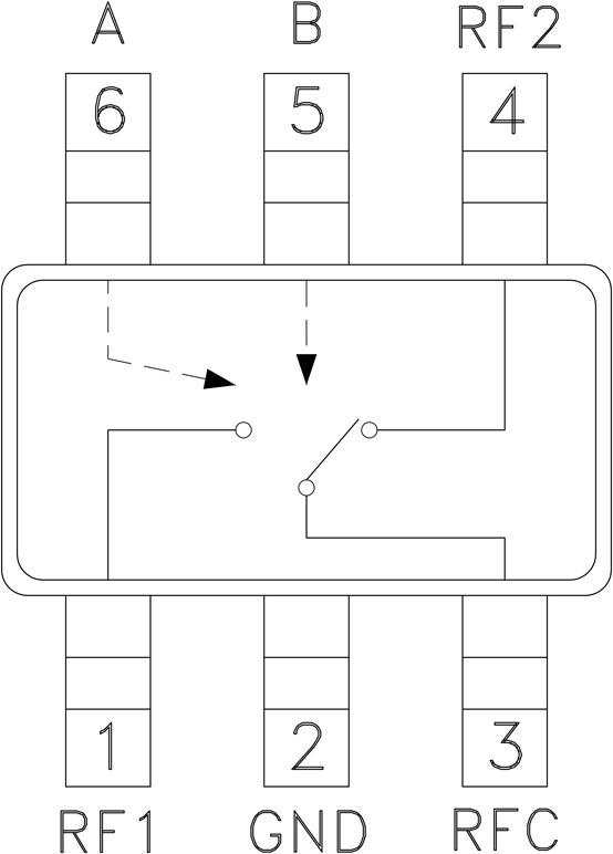
EVAL01-HMC197B
Analog Devices Inc.The HMC197B(E) is a low-cost SPDT switch in a 6-lead SOT26 plastic package for use in general switching applications which require very low insertion loss and very small size. The device can control signals from DC to 3 GHz and is especially suited for 900 MHz, 1.8 - 2.2 GHz, and 2.4 GHz ISM applications with less than 1 dB loss. The design provides exceptional insertion loss performance, ideal for filter and receiver switching. RF1 and RF2 are reflective shorts when ?Off?. The two control voltages require a minimal amount of DC current and offer compatibility with most CMOS & TTL logic families. See HMC221B for same performance in an alternate SOT26 pin-out.APPLICATIONS MMDS & WirelessLAN PCMCIA Wireless Cards Portable WIreless

EVAL01-HMC749LC3C
Analog Devices Inc.The HMC749LC3C is a T Flip-Flop w/Reset designed to support clock frequencies as high as 26 GHz. During normal operation, with the reset pin not asserted, the output toggles from its prior state on the positive edge of the clock. This results in a divide-by two function of the clock input. Asserting the reset pin forces the Q output low regardless of the clock edge state (asynchronous reset assertion). Reversing the clock inputs allows for negative-edge triggered applications. The HMC749LC3C also features an output level control pin, VR, which allows for loss compensation or for signal level optimization.All input signals to the HMC749LC3C are terminated with 50 to Vcc on-chip, and may be either AC or DC coupled. inputs or outputs can be connected directly to a 50 Vcc terminated system, while DC blocking capacitors may be used if the terminating system is 50? ground. The HMC749LC3C operates from a single +3.3V DC supply and is available in a ceramic RoHS compliant 3x3 mm SMT package.APPLICATIONS Serial Data Transmission up to 26 Gbps High Speed Frequency Divider?(up to 26 GHz) Broadband Test & Measurement RF ATE Applications

EVAL01-HMC834LP6GE
Analog Devices Inc.The HMC834LP6GE is a low noise, wide band, Fractional-N Phase-Locked-Loop (PLL) that features an integrated Voltage Controlled Oscillator (VCO) with a fundamental frequency of 2800 MHz - 4200 MHz, and an integrated VCO Output Divider (divide by 1/2/4/6.../60/62) and doubler, that together allow the HMC834LP6GE to generate frequencies from 45 MHz to 1050 MHz, from 1400 MHz to 2100 MHz, from 2800 MHz to 4200 MHz, and from 5600 MHz to 8400 MHz. The integrated Phase Detector (PD) and delta-sigma modulator, capable of operating at up to 100 MHz, permit wider loop-bandwidths with excellent spectral performance.The HMC834LP6GE features industry leading phase noise and spurious performance, across all frequencies, that enable it to minimize blocker effects, and improve receiver sensitivity and transmitter spectral purity. The superior noise floor (< -170 dBc/Hz) makes the HMC834LP6GE an ideal source for a variety of applications - such as; LO for RF mixers, a clock source for high-frequency data-converters, or a tunable reference source for ultra-low spurious applications.Additional features of the HMC834LP6GE include RF output power control from 0 to 6 dB (~2 dB steps), output Mute function, and a delta-sigma modulator Exact Frequency Mode which enables users to generate output frequencies with 0 Hz frequency error.Applications Cellular/4G, WiMax Infrastructure Repeaters and Femtocells Communications Test Equipment CATV Equipment Phased Array Applications DDS Replacement Very High Data Rate Radios Tunable Reference Source for?Spurious- Free Performance

EVAL02-HMC837LP6CE
Analog Devices Inc.The HMC837LP6CE is a fully functioned Fractional-N Phase-Locked-Loop (PLL) Frequency Synthesizer with an Integrated Voltage Controlled Oscillator (VCO). The synthesizer consists of an integrated low noise VCO with a triband output, an autocalibration subsystem for low voltage VCO tuning, a very low noise digital Phase Detector (PD), a precision controlled charge pump, a low noise reference path divider and a fractional divider.The fractional synthesizer features an advanced delta-sigma modulator design that allows both ultra-fine step sizes and low spurious products. The phase detector (PD) features cycle slip prevention (CSP) technology to allow faster frequency hopping times. Ultra low in-close phase noise and low spurious also allows wider loop bandwidths for faster frequency hopping and low micro-phonics.For theory of operation and register map refer to the 'PLLs with Integrated VCO - RF VCOs' Operating Guide.Applications Cellular/4G Infrastructure Repeaters & Femtocells Communications?Test Equipment CATV Equipment Phased Array Applications DDS Replacement? Very High Data Rate Radios


