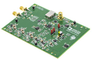
EVAL02-HMC837LP6CE
Analog Devices Inc.The HMC837LP6CE is a fully functioned Fractional-N Phase-Locked-Loop (PLL) Frequency Synthesizer with an Integrated Voltage Controlled Oscillator (VCO). The synthesizer consists of an integrated low noise VCO with a triband output, an autocalibration subsystem for low voltage VCO tuning, a very low noise digital Phase Detector (PD), a precision controlled charge pump, a low noise reference path divider and a fractional divider.The fractional synthesizer features an advanced delta-sigma modulator design that allows both ultra-fine step sizes and low spurious products. The phase detector (PD) features cycle slip prevention (CSP) technology to allow faster frequency hopping times. Ultra low in-close phase noise and low spurious also allows wider loop bandwidths for faster frequency hopping and low micro-phonics.For theory of operation and register map refer to the 'PLLs with Integrated VCO - RF VCOs' Operating Guide.Applications Cellular/4G Infrastructure Repeaters & Femtocells Communications?Test Equipment CATV Equipment Phased Array Applications DDS Replacement? Very High Data Rate Radios
EVAL-24TSSOPEBZ
Analog Devices Inc.The ADG1414 is a monolithic complementary metal oxide semiconductor (CMOS) device containing eight independently selectable switches designed on an industrial CMOS (iCMOS?) process. iCMOS is a modular manufacturing process combining high voltage CMOS and bipolar technologies. iCMOS components can tolerate high supply voltages while providing increased performance, dramatically lower power consumption, and reduce the package size.The ADG1414 is a set of octal SPST (single-pole, single-throw) switches controlled via a 3-wire serial interface. On resistance is closely matched between switches and is very flat over the full signal range. Each switch conducts equally well in both directions and the input signal range extends to the supplies.Data is written to these devices in the form of eight bits; each bit corresponds to one channel.The ADG1414 utilizes a versatile 3-wire serial interface that operates at clock rates of up to 50 MHz and is compatible with standard SPI?, QSPI?, MICROWIRE?, and DSP interface standards. The output of the shift register, SDO, enables a number of these parts to be daisy chained.On power-up, all switches are in the off condition, and the internal registers contain all zeros.PRODUCT HIGHLIGHTS 50 MHz serial interface. 9.5 ? on resistance. 1.6 ? on-resistance flatness. 24-lead TSSOP and 4 mm ? 4 mm LFCSP packages.APPLICATIONS Automatic test equipment Data acquisition systems Battery-powered systems Sample-and-hold systems Audio signal routing Video signal routing Communication systems
EVAL-2LCANRS485EBZ
Analog Devices Inc.The ADM3053 is an isolated controller area network (CAN) physical layer transceiver with an integrated isolated dc-to-dc converter. The ADM3053 complies with the ISO 11898 standard.The device employs Analog Devices, Inc., iCoupler? technology to combine a 2-channel isolator, a CAN transceiver, and Analog Devices isoPower? dc-to-dc converter into a single SOIC surface mount package. An on-chip oscillator outputs a pair of square waveforms that drive an internal transformer to provide isolated power. The device is powered by a single 5 V supply realizing a fully isolated CAN solution.The ADM3053 creates a fully isolated interface between the CAN protocol controller and the physical layer bus. It is capable of running at data rates of up to 1 Mbps.The device has current limiting and thermal shutdown features to protect against output short circuits. The part is fully specified over the industrial temperature range and is available in a 20-lead, wide-body SOIC package.The ADM3053 contains isoPower technology that uses high frequency switching elements to transfer power through the transformer. Special care must be taken during printed circuit board (PCB) layout to meet emissions standards. Refer to the AN-0971 Application Note, Control of Radiated Emissions with?isoPower Devices, for details on board layout considerations.Applications CAN data buses Industrial field networks
EVAL-AD1940AZ
Analog Devices Inc.The AD1940 /?AD1941 are a complete 28-bit, single-chip, multi-channel audio SigmaDSP? for equalization, multiband dynamic processing, delay compensation, speaker compensation, and image enhancement. These algorithms can be used to compen-sate for the real world limitations of speakers, amplifiers, and listening environments, resulting in a dramatic improvement of perceived audio quality.The signal processing used in the AD1940 / AD1941 is comparable to that found in high end studio equipment. Most of the processing is done in full, 56-bit double-precision mode, resulting in very good, low level signal performance and the absence of limit cycles or idle tones. The dynamics processor uses a sophisticated, multiple-breakpoint algorithm often found in high end broadcast compressors. The AD1940 / AD1941 are a fully programmable DSP. Easy to use software allows the user to graphically configure a custom signal processing flow using blocks such as biquad filters, dynamics processors, and surround sound processors. An extensive control port allows click-free parameter updates, along with readback capability from any point in the algorithm flow.The AD1940 / AD1941?s digital input and output ports allow a glueless connection to ADCs and DACs by multiple, 2-channel serial data streams or TDM data streams. When in TDM mode, the AD1940 / AD1941 can input 8 or 16 channels of serial data, and can output 8 or 16 channels of serial data. The input and output port configurations can be individually set. The AD1940 is controlled by a 4-wire SPI? port; the AD1941 is controlled by a 2-wire I2C? bus. Other than the control interface, the functions of the two parts are identical. APPLICATIONS Automotive sound systems Digital televisions Home theater systems (Dolby digital/DTS postprocessor) Multichannel audio systems Mini-component stereos Multimedia audio Digital speaker crossover Musical instruments In-seat sound systems (aircrafts/motor coaches)
EVAL-AD2S1210SDZ
Analog Devices Inc.The AD2S1210 is a complete 10-bit to 16-bit resolution tracking resolver-to-digital converter, integrating an on-board programmable sinusoidal oscillator that provides sine wave excitation for resolvers.The converter accepts 3.15 V p-p ? 27% input signals, in the range of 2 kHz to 20 kHz on the sine and cosine inputs. A Type II servo loop is employed to track the inputs and convert the input sine and cosine information into a digital representation of the input angle and velocity. The maximum tracking rate is 3125 rps.The AD2S1210WDSTZ and the AD2S1210WDSTZRL7 models have been approved by an independent accredited body for use in Automotive Safety Integrity Level B rated applications according to ISO 26262. Contact your local Analog Devices, Inc., sales office to obtain a copy of the safety manual and ASIL B safety assessment certificate. PRODUCT HIGHLIGHTS Ratiometric tracking conversion. The Type II tracking loop provides continuous output position data without conversion delay. It also provides noise immunity and tolerance of harmonic distortion on the reference and input signals. System fault detection. A fault detection circuit can sense loss of resolver signals, out-of-range input signals, input signal mismatch, or loss of position tracking. The fault detection threshold levels can be individually programmed by the user for optimization within a particular application. Input signal range. The sine and cosine inputs can accept differential input voltages of 3.15 V p-p ? 27%. Programmable excitation frequency. Excitation frequency is easily programmable to a number of standard frequencies between 2 kHz and 20 kHz. Triple format position data. Absolute 10-bit to 16-bit angular position data is accessed via either a 16-bit parallel port or a 4-wire serial interface. Incremental encoder emulation is in standard A-quad-B format with direction output available. Digital velocity output. 10-bit to 16-bit signed digital velocity accessed via either a 16-bit parallel port or a 4-wire serial interface. APPLICATIONS DC and ac servo motor control Encoder emulation Electric power steering Electric vehicles Integrated starter generators/alternators Automotive motion sensing and control
EVAL-AD3542RFMCZ
Analog Devices Inc.The AD3542R is a low drift, dual channel, ultra-fast, 16-bit accuracy, voltage output digital-to-analog converter (DAC) that can be configured in multiple voltage span ranges. The AD3542R operates with a fixed 2.5 V reference.The device incorporates three drift compensating feedback resistors for the internal transimpedance amplifier (TIA) that scales the output voltage. Offset and gain scaling registers allow for generation of multiple output span ranges, such as 0 V to 2.5 V, 0 V to 5 V, 0 V to 10 V, ?5 V to +5 V, and ?2.5 V to +7.5 V.The DAC can operate in fast mode for maximum speed or precision mode for maximum accuracy.The serial peripheral interface (SPI) can be configured in single SPI (classic SPI) mode, dual SPI mode and synchronous dual SPI mode with single date rate (SDR) or double data rate (DDR), with logical levels from 1.2 V to 1.8 V.To improve device robustness, cyclic redundancy check (CRC) can be enabled. Multiple error checkers have also been integrated to detect VREF failures or memory map corruption.The AD3542R is specified over the extended industrial temperature range (?40?C to +105?C).APPLICATIONS Instrumentation Hardware in the loop Process control equipment Medical devices Automated test equipment Data acquisition system Programmable voltage sources Optical communications
EVAL-AD4000FMCZ
Analog Devices Inc.The AD4000/AD4004/AD4008 are high accuracy, high speed, low power, 16-bit, Easy Drive, precision successive approximation register (SAR) analog-to-digital converters (ADCs) that operate from a single power supply, VDD. The reference voltage, VREF, is applied externally and can be set independent of the supply voltage. The AD4000/AD40004/AD4008 power scales linearly with throughput. Easy Drive features reduce both signal chain complexity and power consumption while enabling higher channel density. The reduced input current, particularly in high-Z mode, coupled with a long signal acquisition phase, eliminates the need for a dedicated ADC driver. Easy Drive broadens the range of companion circuitry that is capable of driving these ADCs (see Figure 2 in the data sheet). Input span compression eliminates the need to provide a negative supply to the ADC driver amplifier while preserving access to the full ADC code range. The input overvoltage clamp protects the ADC inputs against overvoltage events, minimizing disturbances on the reference pin and eliminating the need for external protection diodes. Fast device throughput up to 2 MSPS allows users to accurately capture high frequency signals and to implement oversampling techniques to alleviate the challenges associated with antialias filter designs. Decreased serial peripheral interface (SPI) clock rate requirements reduce digital input and output power consumption, broadens digital host options, and simplifies the task of sending data across digital isolation. The SPI-compatible serial user interface is compatible with 1.8 V, 2.5 V, 3 V, and 5 V logic by using the separate VIO logic supply.APPLICATIONS Automated test equipment Machine automation Medical equipment Battery-powered equipment Precision data acquisition systems Instrumentation and control systems
EVAL-AD4111SDZ
Analog Devices Inc.The AD4111 is a low power, low noise, 24-bit, sigma-delta (?-?) analog-to-digital converter (ADC) that integrates an analog front end (AFE) for fully differential or single-ended, high impedance (?1 M?) bipolar, ?10 V voltage inputs, and 0 mA to 20 mA current inputs.The AD4111 also integrates key analog and digital signal conditioning blocks to configure eight individual setups for each analog input channel in use. The AD4111 features a maximum channel scan rate of 6.21 kSPS (161 ?s) for fully settled data.The embedded 2.5 V, low drift (5 ppm/?C), band gap internal reference (with output reference buffer) reduces the external component count.The digital filter allows flexible settings, including simultaneous 50 Hz and 60 Hz rejection at a 27.27 SPS output data rate. The user can select between the different filter settings depending on the demands of each channel in the application. The automatic channel sequencer enables the ADC to switch through each enabled channel.The precision performance of the AD4111 is achieved by integrating the proprietary iPassives? technology from Analog Devices, Inc. The AD4111 is factory calibrated to achieve a high degree of specified accuracy.The AD4111 also has the unique feature of open wire detection on the voltage inputs for system level diagnostics using a single 5 V or 3.3 V power supply.The AD4111 operates with a single power supply, making it easy to use in galvanically isolated applications. The specified operating temperature range is ?40?C to +105?C. The AD4111 is housed in a 40-lead, 6 mm ? 6 mm LFCSP package.APPLICATIONS Process control PLC and DCS modules Instrumentation and measuremen
EVAL-AD4116ASDZ
Analog Devices Inc.The AD4116 is a low power, low noise, 24-bit, ?-? analog-to-digital converter (ADC) that integrates an analog front end (AFE) for six fully differential or eleven single-ended, high impedance (?10 M?) bipolar, ?10 V voltage inputs. The additional two differential or four single-ended/pseudo differential direct ADC inputs provides excellent performance at lower input ranges.The AD4116 also integrates key analog and digital signal conditioning blocks to configure eight individual setups for each analog input channel in use. As many as 16 channels can be enabled at any time. A channel is defined as any of the standard analog voltage inputs or a low level direct ADC input. The AD4116 features a maximum channel scan rate of 12,422 SPS (80 ?s) using a sinc5 + sinc1 filter and 20,618 SPS per channel (48 ?s) using a sinc3 filter.The embedded 2.5 V, low drift (5 ppm/?C), band gap internal reference (with output reference buffer) reduces the external component count.The digital filter allows flexible settings, including simultaneous 50 Hz and 60 Hz rejection at a 27.27 SPS output data rate. The user can select between the different filter settings depending on the demands of each channel in the application. The automatic channel sequencer enables the ADC to switch through each enabled channel.The precision performance of the AD4116 is achieved by integrating the proprietary iPassives? technology from Analog Devices, Inc.The AD4116 operates with a single power supply, making it easy to use in galvanically isolated applications. The specified operating temperature range is ?40?C to +105?C. The AD4116 is housed in a 40-lead, 6 mm ? 6 mm LFCSP.APPLICATIONS Process control PLC and DCS modules Instrumentation and measurement
EVAL-AD4630-24-KTZ
Analog Devices Inc.The AD4630-24 is a two-channel, simultaneous sampling, Easy Drive, 2 MSPS successive approximation register (SAR) analog-to-digital converter (ADC). With a guaranteed maximum ?0.9 ppm INL and no missing codes at 24-bits, the AD4630-24 achieves unparalleled precision from ?40?C to +125?C. Figure 1 in the data sheet shows the functional architecture of the AD4630-24.A low-drift, internal precision reference buffer eases voltage reference sharing with other system circuitry. The AD4630-24 offers a typical dynamic range of 106 dB when using a 5 V reference. The low noise floor enables signal chains requiring less gain and lower power. A block averaging filter with programmable decimation ratio can increase dynamic range up to 153 dB. The wide differential input and common mode ranges allow inputs to use the full ?VREF range without saturating, simplifying signal conditioning requirements and system calibration. The improved settling of the Easy Drive analog inputs broadens the selection of analog front-end components compatible with the AD4630-24. Both single-ended and differential signals are supported.The versatile Flexi-SPI serial interface eases host processor and ADC integration. A wide data clocking window, multiple SDO lanes, and optional dual data rate (DDR) data clocking can reduce the serial clock to 10 MHz while operating at a sample rate of 2 MSPS. Echo clock mode and ADC master clock mode relax the timing requirements and simplify the use of digital isolators.The 64-ball chip scale package ball grid array (CSP_BGA) of the AD4630-24 integrates all critical power supply and reference bypass capacitors, reducing the footprint and system component count, and lessening sensitivity to board layout.APPLICATIONS Automatic test equipment Digital control loops Medical instrumentation Seismology Semiconductor manufacturing Scientific instrumentation
EVAL-AD5062SDZ
Analog Devices Inc.The AD5062, a member of ADI?s?nanoDAC? family, is a low power, single 16-bit unbuffered voltage-out DAC that operatesfrom a single 2.7 V to 5.5 V supply. The part offers a relative accuracy specification of ?1 LSB, and operation is guaranteed monotonic with a ?1 LSB DNL specification. The part uses a versatile 3-wire serial interface that operates at clock rates up to 30 MHz, and is compatible with standard SPI?, QSPI?, MICROWIRE?, and DSP interface standards. The reference for the AD5062 is supplied from an external VREF pin. A reference buffer is also provided on-chip. The part incorporates a power-on reset circuit that ensures the DAC output powers up to zero scale or mid-scale and remains there until a valid write takes place to the device. The part contains a power-down feature that reduces the current consumption of the device to typically 300 nA at 5 V and provides software-selectable output loads while in power-down mode. The part is put into power-down mode over the serial interface. Total unadjusted error for the part is
EVAL-AD5064EBZ
Analog Devices Inc.The AD5024 / AD5044 / AD5064 are low power, quad 12-/14-/ 16-bit buffered voltage output?nanoDAC? DACs that offer relative accuracy specifications of 1 LSB INL and 1 LSB DNL with individual reference pins and can operate from a single 4.5 V to 5.5 V supply. The AD5024 / AD5044 / AD5064 parts also offer a differential accuracy specification of ?1 LSB. The parts use a versatile 3-wire, low power Schmitt trigger serial interface that operates at clock rates up to 50 MHz and is compatible with standard SPI, QSPI?, MICROWIRE?, and DSP interface standards. Integrated reference buffers and output amplifiers are also provided on-chip. The AD5024 / AD5044 / AD5064 / AD5064-1 incorporate a power-on reset circuit that ensures the DAC output powers up to zero scale or midscale and remains there until a valid write takes place to the device. The AD5024 / AD5044 / AD5064 / AD5064-1 contain a power-down feature that reduces the current consumption of the device to typically 400 nA at 5 V and provides software selectable output loads while in power-down mode. Total unadjusted error for the parts is
EVAL-AD5116EBZ
Analog Devices Inc.The AD5116 provides a nonvolatile digital potentiometer solution for 64-position adjustment applications, offering guaranteed low resistor tolerance errors of ?8% and up to ?6 mA current density in the A, B, and W pins. The low resistor tolerance, low nominal temperature coefficient, and high bandwidth simplify open-loop applications, as well as tolerance matching applications.The new low A-W and B-W resistance feature minimizes the wiper resistance in the extremes of the resistor array to typically 45 ?.A simple push button interface allows manual control with just two external push button switches. The AD5116 is designed with a built-in adaptive debouncer that ignores invalid bounces due to contact bounce (commonly found in mechanical switches). The debouncer is adaptive, accommodating a variety of push buttons.The AD5116 can automatically save the last wiper position into EEPROM, making it suitable for applications that require a power-up in the last wiper position, for example, audio equipment.The AD5116 is available in a 2 mm ? 2 mm 8-lead LFCSP package. The part is guaranteed to operate over the extended industrial temperature range of ?40?C to +125?C.APPLICATIONS Mechanical potentiometer replacement Portable electronics level adjustment Audio volume control Low resolution DAC LCD panel brightness and contrast control Programmable voltage to current conversion Programmable filters, delays, time constants Feedback resistor programmable power supply Sensor calibration
EVAL-AD5142ADBZ
Analog Devices Inc.The AD5122A/AD5142A potentiometers provide a nonvolatile solution for 128-/256-position adjustment applications, offering guaranteed low resistor tolerance errors of ?8% and up to ?6 mA current density in the Ax, Bx, and Wx pins.The low resistor tolerance and low nominal temperature coefficient simplify open-loop applications as well as applications requiring tolerance matching.The linear gain setting mode allows independent programming of the resistance between the digital potentiometer terminals, through RAW and RWB the string resistors, allowing very accurate resistor matching.The high bandwidth and low total harmonic distortion (THD) ensure optimal performance for ac signals, making it suitable for filter design.The low wiper resistance of only 40 ? at the ends of the resistor array allows for pin-to-pin connection.The wiper values can be set through an I2C-compatible digital interface that is also used to read back the wiper register and EEPROM contents.The AD5122A/AD5142A are available in a compact, 16-lead, 3 mm ? 3 mm LFCSP and a 16-lead TSSOP. The parts are guaranteed to operate over the extended industrial temperature range of ?40?C to +125?C.APPLICATIONS Portable electronics level adjustment LCD panel brightness and contrast controls Programmable filters, delays, time constants Programmable power supplies
EVAL-AD5143DBZ
Analog Devices Inc.The AD5123/AD5143 potentiometers provide a nonvolatilesolution for 128-/256-position adjustment applications, offeringguaranteed low resistor tolerance errors of ?8% and up to ?6 mAcurrent density in the Ax, Bx, and Wx pins.The low resistor tolerance and low nominal temperature coefficientsimplify open-loop applications as well as applications requiringtolerance matching.The linear gain setting mode allows independent programmingof the resistance between the digital potentiometer terminals,through the RAW and RWB string resistors, allowing very accurateresistor matching.The high bandwidth and low total harmonic distortion (THD)ensure optimal performance for ac signals, making the devicessuitable for filter design.The low wiper resistance of only 40 ? at the ends of the resistorarray allows for pin to pin connection.The wiper values can be set through an I2C-compatible digitalinterface that also reads back the wiper register and EEPROMcontents.The AD5123/AD5143 are available in a compact, 16-lead, 3 mm ?3 mm LFCSP. The devices are guaranteed to operate over theextended industrial temperature range of ?40?C to +125?C. APPLICATIONS Portable electronics level adjustment LCD panel brightness and contrast controls Programmable filters, delays, time constants Programmable power supplies
EVAL-AD5160DBZ
Analog Devices Inc.The AD5160 provides a compact 2.9 mm ? 3 mm packaged solution for 256-position adjustment applications. These devices perform the same electronic adjustment function as mechanical potentiometers1 or variable resistors but with enhanced resolution, solid-state reliability, and superior low temperature coefficient performance.The wiper settings are controllable through an SPI-compatible digital interface. The resistance between the wiper and either end point of the fixed resistor varies linearly with respect to the digital code transferred into the RDAC latch.Operating from a 2.7 V to 5.5 V power supply and consuming less than 5 ?A allows for usage in portable battery-operated applications.
EVAL-AD5204SDZ
Analog Devices Inc.The AD5204/AD5206 provide 4-/6-channel, 256-position digitally controlled variable resistor (VR) devices. These devices perform the same electronic adjustment function as a potentiometer or variable resistor. Each channel of the AD5204/AD5206 contains a fixed resistor with a wiper contact that taps the fixed resistor value at a point determined by a digital code loaded into the SPI-compatible serial-input register. The resistance between the wiper and either endpoint of the fixed resistor varies linearly with respect to the digital code transferred into the VR latch. The variable resistor offers a completely programmable value of resistance between the A terminal and the wiper or the B terminal and the wiper. The fixed A-to-B terminal resistance of 10 k?, 50 k?, or 100 k? has a nominal temperature coefficient of 700 ppm/?C.Each VR has its own VR latch that holds its programmed resistance value. These VR latches are updated from an internal serial-to-parallel shift register that is loaded from a standard 3-wire serial-input digital interface. Eleven data bits make up the data-word clocked into the serial input register. The first three bits are decoded to determine which VR latch is loaded with the last eight bits of the data-word when the CS strobe is returned to logic high. A serial data output pin at the opposite end of the serial register (AD5204 only) allows simple daisy chaining in multiple VR applications without requiring additional external decoding logic.An optional reset (PR) pin forces all the AD5204 wipers to the midscale position by loading 0x80 into the VR latch.The AD5204/AD5206 are available in the 24-lead surface-mount SOIC and TSSOP packages. The AD5204 is also available in a 32-lead, 5 mm ? 5 mm LFCSP package. All parts are guaranteed to operate over the extended industrial temperature range of ?40?C to +85?C. For additional single-, dual-, and quad-channel devices, see the AD8400/AD8402/AD8403 data sheets.APPLICATIONS Mechanical potentiometer replacement Instrumentation: gain, offset adjustment Programmable voltage-to-current conversion Programmable filters, delays, time constants Line impedance matching
EVAL-AD5292DBZ
Analog Devices Inc.The AD5291 and AD5292 are single-channel, 256-/1024-position digital potentiometers that combine industry leading variable resistor performance with nonvolatile memory (NVM) in a compact package. These devices are capable of operating across a wide voltage range, supporting both dual supply operation?at ?10.5 V to ?16.5 V and single supply operation at +21 V to +33 V, while ensuring less than 1% end-to-end resistor tolerance error and offering 20-time programmable (20-TP) memory.The guaranteed industry leading low resistor tolerance error?feature simplifies open-loop applications as well as precision?calibration and tolerance matching applications.The AD5291 and AD5292 device wiper settings are controllable?through the SPI digital interface. Unlimited adjustments are?allowed before programming the resistance value into the 20-TP memory. The AD5291 and AD5292 do not require any?external voltage supply to facilitate fuse blow, and there are 20 opportunities for permanent programming. During 20-TP activation, a permanent blow fuse command freezes the wiper?position (analogous to placing epoxy on a mechanical trimmer).The AD5291 and AD5292 are available in a compact 14-lead?TSSOP package. The part is guaranteed to operate over the?extended industrial temperature range of ?40?C to +105?C.APPLICATIONS Mechanical potentiometer replacement Instrumentation: gain and offset adjustment Programmable voltage-to-current conversion Programmable filters, delays, and time constants Programmable power supply Low resolution DAC replacement Sensor calibration
EVAL-AD5316RDBZ
Analog Devices Inc.The AD5316R, a member of the nanoDAC? family, is a low power,quad, 10-bit buffered voltage output DAC. The device includesa 2.5 V, 2 ppm/?C internal reference (enabled by default) and again select pin giving a full-scale output of 2.5 V (gain = 1) or 5 V(gain = 2). The device operates from a single 2.7 V to 5.5 V supply,is guaranteed monotonic by design, and exhibits less than 0.1%FSR gain error and 1.5 mV offset error performance. The device is available in a 3 mm ? 3 mm lead lead frame chip scale package (LFCSP) and in a thin shrink small outline package (TSSOP).The AD5316R also incorporates a power-on reset circuit and aRSTSEL pin. The RSTSEL pin ensures that the DAC outputs powerup to zero scale or midscale and remain at that level until a validwrite takes place. The device contains a per channel power-down feature that reduces the current consumption of the device in power-down mode to 4 ?A at 3 V.The AD5316R uses a versatile 2-wire serial interface that operatesat clock rates up to 400 kHz and includes a VLOGIC pin intendedfor 1.8 V/3 V/5 V logic.Product Highlights Precision DC Performance. Total unadjusted error (TUE): ?0.1% of FSR maximum Offset error: ?1.5 mV maximum Gain error: ?0.1% of FSR maximum Low Drift 2.5 V On-Chip Reference. 2 ppm/?C typical temperature coefficient 5 ppm/?C maximum temperature coefficient Two Package Options. 3 mm ? 3 mm, 16-lead LFCSP 16-lead TSSOPApplications Digital gain and offset adjustment Programmable attenuators Industrial automation Data acquisition systems
EVAL-AD5323DBZ
Analog Devices Inc.The AD5303?/ AD5313?/ AD5323 are dual 8-/10-/12-bit buffered voltage output DACs in a 16-lead TSSOP package that operate from a single 2.5 V to 5.5 V supply, consuming 230 ?A at 3 V. Their on-chip output amplifiers allow the outputs to swing rail-to-rail with a slew rate of 0.7 V/?s. The AD5313 / AD5323 utilize a versatile 3-wire?serial interface that operates at clock rates up to 30 MHz and is?compatible with standard SPI, QSPI?, MICROWIRE?, and DSP?interface standards The references for the two DACs are derived from two reference pins (one per DAC). These reference inputs may be configured as buffered or unbuffered inputs. The parts incorporate a power-on reset circuit, which ensures that the DAC outputs power up to 0 V and remain there until a valid write to the device takes place. There is also an asynchronous active low CLR pin that clears both DACs to 0 V. The outputs of both DACs may be updated simultaneously using the asynchronous LDAC input. The parts contain a power-down feature that reduces the current consumption of the devices to 200 nA at 5 V (50 nA at 3 V) and provides software-selectable output loads while in power-down mode. The parts may also be used in daisy-chaining applications using the SDO pin.The low power consumption of these parts in normal operation makes them ideally suited to portable battery-operated equipment. The power consumption is 1.5 mW at 5 V and 0.7 mW at 3 V, reducing to 1 ?W in power-down mode.APPLICATIONS Portable battery-powered instruments Digital gain and offset adjustment Programmable voltage and current sources Programmable attenuators


