LT1506CR | 4.5A Switch, 500KHz Step Down Switching Regulator, 4V to 15VIN, 3.3VOUT @ 4A
Analog Devices Inc.DC238A: Demo Board for the LT1506 4.5A, 500kHz Step-Down Switching Regulator.
DC2395A-A
Analog Devices Inc.The LTC2320-16 is a low noise, high speed octal 16?bit successive approximation register (SAR) ADC with differential inputs and wide input common mode range. Operating from a single 3.3V or 5V supply, the LTC2320-16 has an 8VP-P differential input range, making it ideal for applications which require a wide dynamic range with high common mode rejection. The LTC2320-16 achieves ?2LSB INL typical, no missing codes at 16 bits and 82dB SNR.The LTC2320-16 has an onboard low drift (20ppm/?C max) 2.048V or 4.096V temperature-compensated reference. The LTC2320-16 also has a high speed SPI-compatible serial interface that supports CMOS or LVDS. The fast 1.5Msps per channel throughput with no latency makes the LTC2320-16 ideally suited for a wide variety of high speed applications. The LTC2320-16 dissipates only 20mW per channel and offers nap and sleep modes to reduce the power consumption to 26?W for further power savings during inactive periods.Applications High Speed Data Acquisition Systems Communications Optical Networking Multiphase Motor Control
DC2395A-B
Analog Devices Inc.The LTC2324-16 is a low noise, high speed quad 16?bit successive approximation register (SAR) ADC with differential inputs and wide input common mode range. Operating from a single 3.3V or 5V supply, the LTC2324-16 has an 8VP-P differential input range, making it ideal for applications which require a wide dynamic range with high common mode rejection. The LTC2324-16 achieves ?2LSB INL typical, no missing codes at 16 bits and 82dB SNR.The LTC2324-16 has an onboard low drift (20ppm/?C max) 2.048V or 4.096V temperature-compensated reference. The LTC2324-16 also has a high speed SPI-compatible serial interface that supports CMOS or LVDS. The fast 2Msps per channel throughput with no latency makes the LTC2324-16 ideally suited for a wide variety of high speed applications. The LTC2324-16 dissipates only 40mW per channel and offers nap and sleep modes to reduce the power consumption to 26?W for further power savings during inactive periods.Applications High Speed Data Acquisition Systems Communications Optical Networking Multiphase Motor Control
DC2395A-D
Analog Devices Inc.The LTC2320-14 is a low noise, high speed octal 14?bit + sign successive approximation register (SAR) ADC with differential inputs and wide input common mode range. Operating from a single 3.3V or 5V supply, the LTC2320-14 has an 8VP-P differential input range, making it ideal for applications which require a wide dynamic range with high common mode rejection. The LTC2320-14 achieves ?1LSB INL typical, no missing codes at 14 bits and 81dB SNR.The LTC2320-14 has an onboard low drift (20ppm/?C max) 2.048V or 4.096V temperature-compensated reference. The LTC2320-14 also has a high speed SPI-compatible serial interface that supports CMOS or LVDS. The fast 1.5Msps per channel throughput with no latency makes the LTC2320-14 ideally suited for a wide variety of high speed applications. The LTC2320-14 dissipates only 20mW per channel and offers nap and sleep modes to reduce the power consumption to 26?W for further power savings during inactive periods.Applications High Speed Data Acquisition Systems Communications Optical Networking Multiphase Motor Control
DC2395A-E
Analog Devices Inc.The LTC2324-12 is a low noise, high speed quad 12-bit + sign successive approximation register (SAR) ADC with differential inputs and wide input common mode range. Operating from a single 3.3V or 5V supply, the LTC2324- 12 has an 8VP-P differential input range, making it ideal for applications which require a wide dynamic range with high common mode rejection. The LTC2324-12 achieves ?0.5LSB INL typical, no missing codes at 12 bits and 78dB SNR.The LTC2324-12 has an onboard low drift (20ppm/?C max) 2.048V or 4.096V temperature-compensated reference. The LTC2324-12 also has a high speed SPI-compatible serial interface that supports CMOS or LVDS. The fast 2Msps per channel throughput with no latency makes the LTC2324-12 ideally suited for a wide variety of high speed applications. The LTC2324-12 dissipates only 40mW per channel and offers nap and sleep modes to reduce the power consumption to 26?W for further power savings during inactive periods.Applications High Speed Data Acquisition Systems Communications Optical Networking Multiphase Motor Control
DC2402A
Analog Devices Inc.The LT6236/LT6237/LT6238 are single/dual/quad low noise, rail-to-rail output op amps that feature 1.1nV/?Hz input referred noise voltage density and draw only 3.5mA of supply current per amplifier. These amplifiers combine very low noise and supply current with a 215MHz gain bandwidth product and a 70V/?s slew rate. Low noise, fast settling time and low offset voltage make this amplifier optimal to drive low noise, high speed SAR ADCs. The LT6236 includes a shutdown feature that can be used to reduce the supply current to less than 10?A.This amplifier family has an output that swings within 50mV of either supply rail to maximize the signal dynamic range in low supply applications and is specified on 3.3V, 5V and ?5V supplies.The LT6236/LT6237/LT6238 are upgrades to the LT6230/LT6231/LT6232, offering similar performance with reduced wideband noise beyond 100kHz.Applications 16-Bit and 18-Bit SAR ADC Drivers Active Filters Low Noise, Low Power Signal Processing
DC2417A-A
Analog Devices Inc.The LTC4367 protects applications where power supply input voltages may be too high, too low or even negative. It does this by controlling the gate voltages of a pair of external N-channel MOSFETs to ensure that the output stays within a safe operating range.The LTC4367 withstands voltages between ?40V and 100V and has an operating range of 2.5V to 60V, while consuming only 70?A in normal operation.Two comparator inputs allow configuration of the overvoltage (OV) and undervoltage (UV) set points using an external resistive divider. A shutdown pin provides external control for enabling and disabling the MOSFETs as well as placing the device in a low current shutdown state. A fault output indicates that the GATE pin is pulling low when the part is in shutdown or the input voltage is outside the UV and OV set points.The LTC4367 has a 32ms turn-on delay that debounces live connections and blocks 50Hz to 60Hz AC power. For fast recovery after faults, the LTC4367-1 has a reduced turn-on delay of 500?s.Applications Portable InstrumentationIndustrial AutomationAutomotive Surge (Load Dump) ProtectionNetwork Equipment
DC2425A-C
Analog Devices Inc.The LTC2311-14 is a low noise, high speed 14-bit + sign successive approximation register (SAR) ADC with differential inputs and wide input common mode range. Operating from a single 3.3V or 5V supply, the LTC2311- 14 has an 8VP-P differential input range, making it ideal for applications which require a wide dynamic range with high common mode rejection. The LTC2311-14 achieves ?0.75LSB INL typical, no missing codes at 14 bits and 80dB SNR typical.The LTC2311-14 has an onboard low drift (20ppm/?C max) 2.048V or 4.096V temperature compensated reference and provides an external 1.25V buffered reference input. The LTC2311-14 also has a high speed SPI-compatible serial interface that supports CMOS or LVDS. The fast 5Msps throughput with one-cycle latency makes the LTC2311-14 ideally suited for a wide variety of high speed applications. The LTC2311-14 dissipates only 50mW with a 5V supply and offers nap and sleep modes to reduce the power consumption to 5?W for further power savings during inactive periods.Applications High Speed Data Acquisition Systems Communications Remote Data Acquisition Imaging Optical Networking Automotive Multiphase Motor Control
LT6658-1.8 Demo Board | Low Noise, High Current, Precision Reference
Analog Devices Inc.Demonstration circuit 2432B features the LT6658, a precision dual output reference that combines the performance of a low drift low noise reference and a linear regulator. Demonstration circuits are available with 1.25V, 1.8V, 2.5V, 3.0V, 3.3V and 5V output option parts. Both outputs are ideal for driving the precision reference inputs of high resolution ADCs and DACs, even with heavy loading while simultaneously acting as output supplies for powering microcontrollers and other supporting devices. Both outputs have the same precision specifications and A track each other over temperature. Each output can be configured with external resistors to give an output voltage up to 6V.
LT6658-3 Demo Board | Low Noise, High Current, Precision Reference
Analog Devices Inc.Demonstration circuit 2432B features the LT6658, a precision dual output reference that combines the performance of a low drift low noise reference and a linear regulator. Demonstration circuits are available with 1.25V, 1.8V, 2.5V, 3.0V, 3.3V and 5V output option parts. Both outputs are ideal for driving the precision reference inputs of high resolution ADCs and DACs, even with heavy loading while simultaneously acting as output supplies for powering microcontrollers and other supporting devices. Both outputs have the same precision specifications and A track each other over temperature. Each output can be configured with external resistors to give an output voltage up to 6V.
DC2435A-B
Analog Devices Inc.The LTC7813 is a high performance synchronous Boost+Buck DC/DC switching regulator controller that drives all N-channel power MOSFET stages. It contains independent step-up (boost) and step-down (buck) controllers that can regulate two separate outputs or be cascaded to regulate an output voltage from an input voltage that can be above, below, or equal to the output voltage. The LTC7813 operates from a wide 4.5V to 60V input supply range. When biased from the output of the boost regulator, the LTC7813 can operate from an input supply as low as 2.2V after start-up. The 34?A no-load quiescent current (both channels on) extends operating runtime in battery-powered systems.Unlike conventional buck-boost regulators, the LTC7813?s cascaded Boost+Buck solution has continuous, nonpulsating, input and output currents, substantially reducing voltage ripple and EMI. The LTC7813 has independent feedback and compensation points for the boost and buck regulation loops, enabling a fast output transient response that can be externally optimized.Applications Automotive and Industrial Power Systems High Power Battery Operated Systems
DC2440A
Analog Devices Inc.The LTC3374A is a multioutput power supply IC consisting of eight synchronous 1A buck converters, all powered from independent 2.25V to 5.5V input supplies. An upgraded pin-compatible version of the LTC3374, the LTC3374A, has higher efficiency, improved output voltage accuracy and an added overvoltage (OV) indicator.The DC/DCs may be used independently or in parallel to achieve higher output currents of up to 4A with a shared inductor. The common buck switching frequency may be programmed with an external resistor, synchronized to an external oscillator, or set to a default internal 2MHz clock. The operating mode for all DC/DCs may be programmed via the MODE pin.To reduce input noise the buck converters are phased in 90? steps. Precision enable pin thresholds simplify powerup sequencing. The LTC3374A is available in a 38-lead 5mm ? 7mm QFN package as well as a 38-lead exposed pad TSSOP package. NOTES LTC3374 LTC3374A Higher efficiency, improved output voltage accuracy and an added overvoltage (OV) indicator APPLICATIONS General Purpose Multichannel Power Supplies Industrial/Automotive/Communications
LTM4636 High Efficiency, PolyPhase 120A Step-Down Power µModule Regulator
Analog Devices Inc.Demonstration circuit DC2448A-B features a PolyPhase® design using the LTM4636EY, a 40A high efficiency, switch mode step-down power µModule® regulator. The input voltage range is from 4.7V to 15V. When VIN < 5.5V, short PVCC to VIN with R1 = 0Ω, and set R3 = 0Ω and remove R2. The output voltage range is 0.6V to 3.3V. The DC2448A-B can deliver a nominal 120A output current. As explained in the data sheet, output current derating is necessary for certain VIN, VOUT, and thermal conditions. The board operates in continuous conduction mode in heavy load conditions. For high efficiency at low load currents, the MODE_PLLIN jumper selects pulse-skipping mode for noise sensitive applications or Burst Mode® operation in less noise sensitive applications. The MODE_PLLIN pin also allows the LTM4636 to synchronize to an external clock signal. The phases of the three LTM4636s are 0 degrees, 120 degrees and 240 degrees. DC2448A-B has the option of choosing both internal and external compensation circuit for LTM4636. The LTM4636 data sheet must be read in conjunction with this demo manual prior to working on or modifying demo circuit DC2448A-B.
DC2449A-B
Analog Devices Inc.The LT8335 is a current mode DC/DC converter capable of generating either positive or negative output voltages using a single feedback pin. It can be configured as a boost, SEPIC or inverting converter consuming as low as 6?A of quiescent current. Low ripple Burst Mode operation maintains high efficiency down to very low output currents while keeping the output ripple below 15mV in a typical application. The internally compensated current mode architecture results in stable operation over a wide range of input and output voltages. Integrated soft-start and frequency foldback functions are included to control inductor current during start-up. The 2MHz operation combined with the small 8-lead DFN package, enables low cost, area efficient solutions.Applications Industrial and Automotive Telecom Medical Diagnostic Equipment Portable Electronics
DC2450A-B
Analog Devices Inc.The LTC2936 is an EEPROM configurable voltage supervisor which can simultaneously monitor up to six power supply voltage inputs. Each voltage detector offers I2C programmable overvoltage/undervoltage thresholds in various ranges and increments and a dedicated comparator output.Two general purpose inputs (GPI) can be configured as programmable manual reset (MR), UV disable (UVDIS), margin (MARG), Write Protect (WP) or auxiliary comparator (AUXC) inputs. Three general purpose pins (GPIO) can be configured for input or output operation. When configured as an input, a GPIO pin can be mapped to any other GPIO configured as output. The GPIO pins can also be configured as ALERT or fault outputs. Faults can be configured with programmable delay-on-release times. Output type and polarity are also configurable.Status and history registers log faults and can be polled via the I2C interface. A fault snapshot is also backed up in internal EEPROM. All parameters are programmable via the I2C interface. Configuration EEPROM supports autonomous operation without additional software.Applications High Availability Computer Systems Network Servers Telecom Equipment Data Storage
DC2455A-A
Analog Devices Inc.The LTM4650-1A/LTM4650-1B is dual 25A or single 50A output step-down ?Module? (power module) regulator with ?0.8% (LTM4650-1A) and ?1.5% (LTM4650-1B) total DC output error with ?3% transient output error. Included in the package are the switching controller, power FETs, inductors, and all supporting components. External compensation allows for fast transient response to minimize output capacitance when powering FPGAs, ASICs, and processors. With synchronized multiphase parallel current sharing, six LTM4650-1 devices can deliver up to 300A. The LTM4650-1 is offered in a 16mm ? 16mm ? 5.01 BGA package, with SnPb (BGA) or RoHS compliant terminal finish. VIN Range VOUT Range Comp DC VOUT Accy LTM4650 4.5V to 15V 0.6V to 1.8V Internal 1.5% LTM4650-1B 4.5V to 15V 0.6V to 1.8V External 1.5% LTM4650-1A 4.5V to 15V 0.6V to 1.8V External 0.8% LTM4650A 4.5V to 16V 0.6V to 5.5V Internal 1% LTM4650A-1 4.5V to 16V 0.6V to 5.5V External 1% Applications FPGA, ASIC, ?Processor Core Voltage Regulation Information, Communication Systems
DC2459A-A
Analog Devices Inc.The LTC1666/LTC1667/LTC1668 are 12-/14-/16-bit, 50Msps differential current output DACs implemented on a high performance BiCMOS process with laser trimmed, thin-film resistors. The combination of a novel current-steering architecture and a high performance process produces DACs with exceptional AC and DC performance. The LTC1668 is the first 16-bit DAC in the marketplace to exhibit an SFDR (spurious free dynamic range) of 87dB for an output signal frequency of 1MHz.Operating from ?5V supplies, the LTC1666/LTC1667/LTC1668 can be configured to provide full-scale output currents up to 10mA. The differential current outputs of the DACs allow single-ended or true differential operation. The ?1V to 1V output compliance of the LTC1666/LTC1667/LTC1668 allows the outputs to be connected directly to external resistors to produce a differential output voltage without degrading the converter?s linearity. Alternatively, the outputs can be connected to the summing junction of a high speed operational amplifier, or to a transformer.The LTC1666/LTC1667/LTC1668 are pin compatible and are available in a 28-pin SSOP and are fully specified over the industrial temperature range.Applications Cellular Base Stations Multicarrier Base Stations Wireless Communication Direct Digital Synthesis (DDS) xDSL Modems Arbitrary Waveform Generation Automated Test Equipment Instrumentation
DC2464A-A
Analog Devices Inc.The LTC3351 is a backup power controller that charges and monitors a series stack of one to four supercapacitors. The LTC3351?s synchronous step-down controller drives N-channel MOSFETs for constant current/constant voltage charging with programmable input current limit. In addition, the step-down converter runs in reverse as a step-up converter to deliver power from the supercapacitor stack to the backup supply rail. Internal balancers eliminate the need for external balance resistors and each capacitor has a shunt regulator for overvoltage protection.The LTC3351 monitors system voltages, currents, stack capacitance and ESR which can all be read over the I2C/SMBus port. The hot swap controller uses N-channel MOSFETs for inrush control and a low loss path from the input to the output. The ideal diode controller uses an N-channel MOSFET for a low loss power path from the supercapacitors to the output. The LTC3351 is available in a thermally enhanced low profile 44-lead 4mm ? 7mm ? 0.75mm QFN surface mount package.APPLICATIONS Swappable PCIE Cards with NVM High Current 12V Ride-Through UPS Servers/Mass Storage/High Availability Systems
DC2479A-A
Analog Devices Inc.The LTM4650 is a dual 25A or single 50A output switching mode step-down DC/DC ?Module? (power module) regulator. Included in the package are the switching controllers, power FETs, inductors, and all supporting components. Operating from an input voltage range of 4.5V to 15V, the LTM4650 supports two outputs each with an output voltage range of 0.6V to 1.8V, each set by a single external resistor. Its high efficiency design delivers up to 25A continuous current for each output. Only a few input and output capacitors are needed. The LTM4650 is pin compatible with the LTM4620 (dual 13A, single 26A) and the LTM4630 (dual 18A, single 36A).The device supports frequency synchronization, multiphase operation, Burst Mode operation and output voltage tracking for supply rail sequencing and has an onboard temperature diode for device temperature monitoring. High switching frequency and a current mode architecture enable a very fast transient response to line and load changes without sacrificing stability.Fault protection features include overvoltage and overcurrent protection. The LTM4650 is offered in a 16mm ? 16mm ? 5.01mm BGA package. Vin Range Vout Range Comp DC Vout Accy LTM4650 4.5V to 15V 0.6V to 1.8V Internal 1.5% LTM4650-1B 4.5V to 15V 0.6V to 1.8V External 1.5% LTM4650-1A 4.5V to 15V 0.6V to 1.8V External 0.8% LTM4650A 4.5V to 16V 0.6V to 5.5V Internal 1% LTM4650A-1 4.5V to 16V 0.6V to 5.5V External 1% Applications Processor, ASIC and FPGA Core Power Telecom and Networking Equipment Storage and ATCA Cards Industrial Equipment
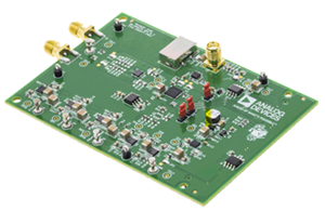
LTC5562 - Low Power Mixer Demo Board Set Up for Downconversion Applications with IF Output Turned to 10MHz to 550MHz
Analog Devices Inc.The LTC5562 is a versatile low power mixer optimized for applications requiring very wide input bandwidth, low distortion, and low LO leakage. This mixer can be used for either upconverting or downconverting applications, and provides a nominal conversion gain of 1dB. Demonstration circuit 2483A-A showcases the LTC5562 mixer for upconverting applications while demonstration circuit 2483A-B is tuned for downconverting applications. The differential inputs are optimized for use with 1:1 transmission- line baluns, allowing very wideband impedance matching. The LTC5562 uses a 3.3V supply for low power consumption and an enable pin allows the part to be shut down for further power savings. The total mixer current is adjustable, allowing for even further power savings. The standard match frequency ranges for each board are outlined in the table below.


