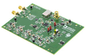
ADCLK925/PCBZ
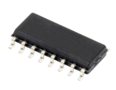
Analog Devices Inc.The ADCLK905 (one input, one output), ADCLK907 (dual oneinput, one output), and ADCLK925 (one input, two outputs) areultrafast clock/data buffers fabricated on the Analog Devices, Inc.,proprietary XFCB3 silicon germanium (SiGe) bipolar process.The ADCLK905/ADCLK907/ADCLK925 feature full-swing emitter coupled logic (ECL) output drivers. For PECL (positive ECL) operation, bias VCC to the positive supply and VEE to ground. For NECL (negative ECL) operation, bias VCC to ground and VEE to the negative supply.The buffers offer 95 ps propagation delay, 7.5 GHz toggle rate, 10 Gbps data rate, and 60 fs random jitter (RJ).The inputs have center tapped, 100 ?, on-chip termination resistors. A VREF pin is available for biasing ac-coupled inputs.The ECL output stages are designed to directly drive 800 mV each side into 50 ? terminated to VCC ? 2 V for a total differential output swing of 1.6 V.The ADCLK905/ADCLK907/ADCLK925 are available in 16-lead LFCSP packages.Applications Clock and data signal restoration and level shifting Automated test equipment (ATE) High speed instrumentation High speed line receivers Threshold detection Converter clocking
ADCLK944/PCBZ
Analog Devices Inc.The ADCLK944 is an ultrafast clock fanout buffer fabricated on the Analog Devices, Inc., proprietary XFCB3 silicon germanium (SiGe) bipolar process. This device is designed for high speed applications requiring low jitter.The device has a differential input equipped with center-tapped, differential, 100 ? on-chip termination resistors. The input can accept dc-coupled LVPECL, CML, 3.3 V CMOS (single-ended), and ac-coupled 1.8 V CMOS, LVDS, and LVPECL inputs. A VREF pin is available for biasing ac-coupled inputs.The ADCLK944 features four full-swing emitter-coupled logic (ECL) output drivers. For LVPECL (positive ECL) operation, bias VCC to the positive supply and VEE to ground. For ECL operation, bias VCC to ground and VEE to the negative supply.The ECL output stages are designed to directly drive 800 mV each side into 50 ? terminated to VCC ? 2 V for a total differential output swing of 1.6 V.The ADCLK944 is available in a 16-lead LFCSP and is specified for operation over the standard industrial temperature range of ?40?C to +85?C.?APPLICATIONS Low jitter clock distribution Clock and data signal restoration Level translation Wireless communications Wired communications Medical and industrial imaging ATE and high performance instrumentation
ADIS16203/PCBZ
Analog Devices Inc.The ADIS16203 is a complete incline-angle measurement system ina single compact package enabled by the Analog Devices, Inc.,iSensor? integration. By enhancing the Analog Devices iMEMS?sensor technology with an embedded signal processing solution, the ADIS16203 provides factory-calibrated, sensor-to-digital incline-angle data in a convenient format that can be accessed using aserial peripheral interface (SPI). The SPI interface provides access to multiple measurements: 360? linear inclination angles, ?180?linear incline angles, temperature, power supply, and one auxiliaryanalog input. Easy access to calibrated digital sensor data providesdevelopers with a system-ready device, reducing developmenttime, cost, and program risk.Unique characteristics of the end system are accommodatedeasily through several built-in features, such as a single-command offset calibration, along with convenient sample rate and band-width control.The ADIS16203 offers the following embedded features that eliminate the need for external circuitry and provide a simplified system interface: Configurable alarm function Auxiliary 12-bit analog-to-digital converter (ADC) Auxiliary 12-bit digital-to-analog converter (DAC) Configurable digital I/O port Digital self-test functionThe ADIS16203 offers two power management features formanaging system-level power dissipation: low power mode anda configurable shutdown feature.The ADIS16203 is available in a 9.2 mm ? 9.2 mm ? 3.9 mmlaminate-based land grid array (LGA) package with a temperature range of ?40?C to +125?C.APPLICATIONS Tilt sensing, inclinometers Platform control, stabilization, and leveling Motion/position measurement Monitor/alarm devices (security, medical, safety) Robotics
ADIS16209/PCBZ
Analog Devices Inc.The ADIS16209 is a high accuracy, digital inclinometer that accommodates both single-axis (?180?) and dual-axis (?90?) operation. The standard supply voltage (3.3 V) and serial peripheral interface (SPI) enable simple integration into most industrial system designs. A simple internal register structure handles all output data and configuration features. This includes access to the following output data: calibrated acceleration, accurate incline angles, power supply, internal temperature, auxiliary analog and digital input signals, diagnostic error flags, and programmable alarm conditions.Configurable operating parameters include sample rate, power management, digital filtering, auxiliary analog and digital output, offset/null adjustment, and self-test for sensor mechanical structure.The ADIS16209 is available in a 9.2 mm ? 9.2 mm ? 3.9 mm LGA package that operates over a temperature range of ?40?C to +125?C. It can be attached using standard RoHS-compliant solder reflow processes.APPLICATIONS Platform control, stabilization, and alignment Tilt sensing, inclinometers, leveling Motion/position measurement Monitor/alarm devices (security, medical, safety) Navigation
ADIS16477-1/PCBZ
Analog Devices Inc.The ADIS16477 is a precision, miniature MEMS inertial measurement unit (IMU) that includes a triaxial gyroscope and a triaxial accelerometer. Each inertial sensor in the ADIS16477 combines with signal conditioning that optimizes dynamic performance. The factory calibration characterizes each sensor for sensitivity, bias, alignment, linear acceleration (gyroscope bias), and point of percussion (accelerometer location). As a result, each sensor has dynamic compensation formulas that provide accurate sensor measurements over a broad set of conditions.The ADIS16477 provides a simple, cost effective method for integrating accurate, multiaxis inertial sensing into industrial systems, especially when compared with the complexity and investment associated with discrete designs. All necessary motion testing and calibration are part of the production process at the factory, greatly reducing system integration time. Tight orthogonal alignment simplifies inertial frame alignment in navigation systems. The serial peripheral interface (SPI) and register structure provide a simple interface for data collection and configuration control.The ADIS16477 is available in a 44-ball, ball grid array (BGA) package that is approximately 11 mm ? 15 mm ? 11 mm.Applications Navigation, stabilization, and instrumentation Unmanned and autonomous vehicles Smart agriculture/construction machinery Factory/industrial automation, robotics Virtual/augmented reality Internet of Moving Things
ADIS16505-2/PCBZ
Analog Devices Inc.The ADIS16505 is a precision, miniature microelectromechanical system (MEMS) inertial measurement unit (IMU) that includes a triaxial gyroscope and a triaxial accelerometer. Each inertial sensor in the ADIS16505 combines with signal conditioning that optimizes dynamic performance. The factory calibration characterizes each sensor for sensitivity, bias, alignment, linear acceleration (gyroscope bias), and point of percussion (accelerometer location). As a result, each sensor has dynamic compensation formulas that provide accurate sensor measurements over a broad set of conditions.The ADIS16505 provides a simplified, cost effective method for integrating accurate, multi-axis inertial sensing into industrial systems, especially when compared with the complexity and investment associated with discrete designs. All necessary motion testing and calibration are part of the production process at the factory, greatly reducing system integration time. Tight orthogonal alignment simplifies inertial frame alignment in navigation systems. The serial peripheral interface (SPI) and register structure provide a simple interface for data collection and configuration control.The ADIS16505 is available in a 100-ball, ball grid array (BGA) package that is approximately 15 mm ? 15 mm ? 5 mm.Applications Navigation, stabilization, and instrumentation Unmanned and autonomous vehicles Smart agriculture and construction machinery Factory/industrial automation, robotics Virtual/augmented reality Internet of Moving Things
ADIS16505-3/PCBZ
Analog Devices Inc.The ADIS16505 is a precision, miniature microelectromechanical system (MEMS) inertial measurement unit (IMU) that includes a triaxial gyroscope and a triaxial accelerometer. Each inertial sensor in the ADIS16505 combines with signal conditioning that optimizes dynamic performance. The factory calibration characterizes each sensor for sensitivity, bias, alignment, linear acceleration (gyroscope bias), and point of percussion (accelerometer location). As a result, each sensor has dynamic compensation formulas that provide accurate sensor measurements over a broad set of conditions.The ADIS16505 provides a simplified, cost effective method for integrating accurate, multi-axis inertial sensing into industrial systems, especially when compared with the complexity and investment associated with discrete designs. All necessary motion testing and calibration are part of the production process at the factory, greatly reducing system integration time. Tight orthogonal alignment simplifies inertial frame alignment in navigation systems. The serial peripheral interface (SPI) and register structure provide a simple interface for data collection and configuration control.The ADIS16505 is available in a 100-ball, ball grid array (BGA) package that is approximately 15 mm ? 15 mm ? 5 mm.Applications Navigation, stabilization, and instrumentation Unmanned and autonomous vehicles Smart agriculture and construction machinery Factory/industrial automation, robotics Virtual/augmented reality Internet of Moving Things
ADL5205-EVALZ
Analog Devices Inc.The ADL5205 is a digitally controlled, wide bandwidth, variable gain dual amplifier (DGA) that provides precise gain control, high output third-order intercept (OIP3) and a near constant noise figure for the first 12 dB of attenuation. The excellent OIP3 performance of 48.5 dBm (at 200 MHz, 5 V, high performance mode, and maximum gain) makes the ADL5205 an excellent gain control device for a variety of receiver applications.For wide input dynamic range applications, the ADL5205 provides a broad 35 dB gain range with a 1 dB step size. The gain is adjustable through multiple gain control and interface options: parallel, SPI, or gain step up/down control.The two channels of the ADL5205 can be powered up independently by applying the appropriate logic level to the PWUPA and PWUPB pins. The quiescent current of the ADL5205 is typically 175 mA for high performance mode and 135 mA for?low power mode. When disabled, the ADL5205 consumes only 14 mA and offers excellent input to output isolation. The gain setting is preserved when the device is disabled.Fabricated on the Analog Devices, Inc., high speed, silicon germanium (SiGe) complementary BiCMOS process, the ADL5205 provides precise gain adjustment capabilities with good distortion performance. The ADL5205 amplifier comes in a compact, thermally enhanced, 6 mm ? 6 mm, 40-lead LFCSP package and operates over the temperature range of ?40?C to +85?C.Note that throughout this data sheet, multifunction pins, such as CSA/A3, are referred to by the entire pin name or by a single function of the pin, for example, CSA, when only that function is relevant.Applications Differential analog-to-digital converter (ADC) drivers High intermediate frequency (IF) sampling receivers High output power IF amplification Instrumentation
ADL5306-EVAL
Analog Devices Inc.The ADL5306 is a low cost micro-miniature logarithmic converter optimized for the determination of optical power in fiber-optic systems. It uses an advanced implementation of a classic translinear (junction-based) technique to provide a large dynamic range in a versatile and easily-used form. A single supply voltage of between 3 V and 5.5 V is adequate; dual supplies may optionally be used. The low quiescent current (typically 5 mA) permits use in battery-operating applicationsThe input current IPD of 100 nA to 100 ?A applied to the INPT pin is the collector current of an optimally-scaled NPN transistor, which converts this current to a voltage (its VBE) with a precise logarithmic relationship. A second such converter is used to handle the reference current, IREF, applied to pin IREF. These input nodes are biased slightly above ground (0.5 V). This is generally acceptable for photodiode applications where the anode does not need to be grounded. Similarly, this bias voltage is easily accounted for in generating IREF. The output of the logarithmic front-end is available at pin VLOG.
ADL5330-EVALZ
Analog Devices Inc.The ADL5330 is a high performance, voltage controlled, variablegain amplifier (VGA)/attenuator for use in applications withfrequencies up to 3 GHz. The balanced structure of the signalpath minimizes distortion while it also reduces the risk ofspurious feedforward at low gains and high frequencies causedby parasitic coupling. While operation between a balanced sourceand load is recommended, a single sided input is internallyconverted to differential form.The input impedance is 50 ? from INHI to INLO. The outputsare usually coupled into a 50 ? grounded load via a 1:1 balun. Asingle supply of 4.75 V to 5.25 V is required.The 50 ? input system converts the applied voltage to a pair ofdifferential currents with high linearity and good commonrejection even when driven by a single sided source. The signalcurrents are then applied to a proprietary voltage controlledattenuator providing precise definition of the overall gain underthe control of the linear in dB interface. The GAIN pin accepts avoltage from 0 V at minimum gain to 1.4 V at full gain with a20 mV/dB scaling factor. The output of the high accuracy wideband attenuator is appliedto a differential transimpedance output stage. The output stagesets the 50 ? differential output impedances and drives theOPHI and OPLO pins. The ADL5330 has a power-downfunction. It can be powered down by a Logic LO input on theENBL pin. The current consumption in power-down mode is250 ?A.The ADL5330 is fabricated on an Analog Devices, Inc.,proprietary high performance, complementary bipolar IC process.The ADL5330 is available in a 24-lead (4 mm ? 4 mm), Pb-freeLFCSP package and is specified for operation from ambienttemperatures of ?40?C to +85?C. An evaluation board is alsoavailable. Applications Transmit and receive power control at RF and IF
ADL5350-EVALZ
Analog Devices Inc.The ADL5350 is a high linearity, up-and-down converting mixer capable of operating over a broad input frequency range. It is well suited for demanding cellular base-station mixer designs that requirehigh sensitivity and effective blocker immunity. Based on a GaAs pHEMT, single-ended mixer architecture, the ADL5350 provides excellent input linearity and low noise figure without the need for a high power level local oscillator (LO) drive.In 850 MHz/900 MHz receive applications, the ADL5350 provides a typical conversion loss of only 6.8 dB. The integrated LO amplifier allows a low LO drive level, typically only 4 dBm for most applications.The input IP3 is typically greater than 25 dBm, with an input compression point of 19 dBm. The high input linearity of the ADL5350 makes the device an excellent mixer for communications systems that require high blocker immunity, such as GSM 850/900 and 800 MHz CDMA2000. At 2 GHz, a slightly greater supply current is required to obtain similar performance.The single-ended broadband RF/IF port allows the device to be customized for a desired band of operation using simple external filter networks. The LO to RF isolation is based on the LO rejection of the RF port filter network. Greater isolation may be achieved by using higher order filter networks, as described in the Applications Information section of this data sheet.The ADL5350 is fabricated on a GaAs pHEMT, high performance IC process. The ADL5350 is available in a 3 mm x 2 mm 8-lead LFCSP. It operates over a ?40?C to +85?C temperature range. An evaluation board is also available.Applications Cellular base station Point-to-point radio links RF instrumentation
ADL5500-EVALZ
Analog Devices Inc.The ADL5500 is a mean-responding power detector for use in high frequency receiver and transmitter signal chains from 100 MHz to 6 GHz. It is easy to apply, requiring only a single supply between 2.7 V and 5.5 V and a power supply decoupling capacitor. The input is internally ac-coupled and has a nominal input impedance of 50 ?. The output is a linear-responding dc voltage with a conversion gain of 6.4 V/V rms at 900 MHz. The on-chip, 1 k? series resistance at the output combined with an external shunt capacitor creates a low-pass filter response that reduces the residual ripple in the dc output voltage.The ADL5500 is intended for true power measurement of simple and complex waveforms. The device is particularly useful for measuring high crest factor (high peak-to-rms ratio) signals, such as CDMA2000, W-CDMA, and QPSK/QAM-based OFDM waveforms.The ADL5500 offers excellent temperature stability with near 0 dB measurement error across temperature. The high accuracy range, centered around +3 dBm at 900 MHz, offers ?0.1 dB error from ?40?C to +85?C over an 8.5 dB range. The ADL5500 reduces calibration requirements with low drift across a 30 dB range over temperature and process variations.The ADL5500 operates from ?40?C to +85?C and is available in a 4-ball, 1.0 mm ? 1.0 mm wafer-level chip scale package. It is fabricated on a proprietary high fT silicon bipolar process.
ADL5505-EVALZ
Analog Devices Inc.The ADL5505 is a TruPwr? mean-responding (true rms) powerdetector for use in high frequency receiver and transmitter signalchains from 450 MHz to 6000 MHz. Requiring only a singlesupply between 2.5 V and 3.3 V, the detector draws less than1.8 mA. The input is internally ac-coupled and has a nominalinput impedance of 500 ?. The rms output is a linear-respondingdc voltage with a conversion gain of 1.86 V/V rms at 900 MHz.The ADL5505 is a highly accurate, easy to use means ofdetermining the rms of complex waveforms. It can be used forpower measurements of both simple and complex waveformsbut is particularly useful for measuring high crest factor (highpeak-to-rms ratio) signals, such as W-CDMA, CDMA2000,WiMAX, WLAN, and LTE waveforms.The on-chip modulation filter provides adequate averaging formost waveforms. An on-chip, 100 ? series resistance at theoutput, combined with an external shunt capacitor, creates a low-passfilter response that reduces the residual ripple in the dc outputvoltage.The ADL5505 offers excellent temperature stability across a30 dB range and near 0 dB measurement error across temperatureover the top portion of the dynamic range. In addition to itstemperature stability, the ADL5505 offers low process variationsthat further reduce calibration complexity.The power detector operates from ?40?C to +85?C and isavailable in an 4-ball, 0.8 mm ? 0.8 mm wafer-level chip scalepackage. It is fabricated on a high fT silicon BiCMOS process.Applications Power measurement of W-CDMA, CDMA2000, QPSK-/QAM-based OFDM (LTE and WiMAX), and other complex modulation waveforms RF transmitter or receiver power measurement
ADL5521-EVALZ
Analog Devices Inc.The ADL5521 is a high performance GaAs pHEMT low noise amplifier. It provides high gain and low noise figure for single-downconversion IF sampling receiver architectures as well as direct-downconversion receivers.The ADL5521 provides a high level of integration by incorporating the active bias and dc blocking capacitors, making it very easy to use while not sacrificing design flexibility.The ADL5521 is easy to tune, requiring only a few external components. The device can support operation from 3 V to 5?V, and the current draw can be adjusted with the external bias resistor for applications requiring low power consumption.The ADL5521 comes in a compact, thermally enhanced, 3 mm ? 3 mm LFCSP and operates over the temperature range of ?40?C to +85?C.A fully populated evaluation board is also available.
ADL5534-EVALZ
Analog Devices Inc.The ADL5534 contains two broadband, fixed-gain, linear amplifiers and operates at frequencies up to 500 MHz. The device can be used in a wide variety of equipment, including cellular, satellite, broadband, and instrumentation equipment.The ADL5534 has a fixed gain of 20 dB, which is stable over frequency, temperature, power supply, and from device-to-device. The amplifiers are single-ended and internally matched to 50 ?. Only input/output ac-coupling capacitors, power supply decoupling capacitors, and an external bias inductor are required for operation of each amplifierThe ADL5534 is fabricated on a GaAs HBT process. The device is packaged in a 16-lead 5 mm ? 5 mm LFCSP that uses an exposed paddle for excellent thermal impedance. The ADL5534 consumes 98 mA of current per amplifier on a single 5 V supply, and is fully specified for operation from ?40?C to +85?C.A similar amplifier, ADL5531 (available from Analog Devices, Inc.) is the 20 dB gain single-channel version. Fully populated evaluation boards for both the ADL5531 and ADL5534 are available.
ADL5535-EVALZ
Analog Devices Inc.The ADL5535 is a 16 dB linear amplifier that operates at frequencies up to 1 GHz. The device can be used in a wide variety of cellular, CATV, military, and instrumentation equipment.The ADL5535 provides the highest dynamic range available from an internally matched IF gain block. This is accomplished by providing extremely low noise figures and very high OIP3 specifications simultaneously across the entire 1 GHz frequency range. The ADL5535 also provides extremely flat gain and P1dB over frequency, which are stable over temperature, power supply, and from device to device.The device is internally matched to 50 ? at the input and output, making the ADL5535 very easy to implement in a wide variety of applications. Only input/output ac coupling capacitors, power supply decoupling capacitors, and an external inductor are required for operation.The ADL5535 is fabricated on a GaAs HBT process and has an ESD rating of ?2 kV (Class 2). The device is assembled in an MSL-1 rated SOT-89 package that uses an exposed paddle for excellent thermal impedance.The ADL5535 consumes only 97 mA on a single 5 V supply and is fully specified for operation from ?40?C to +85?C.The ADL5535 is also pin-compatible with the 20 dB gain ADL5536. Fully populated evaluation boards are available for each amplifier.
ADL5544-EVALZ
Analog Devices Inc.The ADL5544 is a single-ended RF/IF gain block amplifier that provides broadband operation from 30 MHz to 6 GHz. The ADL5544 provides over 34 dBm of OIP3 using only 55 mA from a 5 V supply.The ADL5544 provides a gain of 17 dB, which is stable over frequency, temperature, power supply, and from device to device. The amplifier is offered in the industry-standard SOT-89 package and is internally matched to 50 ? at the input and output, making the ADL5544 very easy to implement in a wide variety of applications. The only external components required are the input/output ac coupling capacitors, power supply decoupling capacitors, and dc bias inductor.The ADL5544 is fabricated on an InGaP HBT process and has a high ESD rating of ?1.5 kV (Class 1C). The ADL5544 is also fully specified for operation across the wide temperature range of ?40?C to +105?C. A fully populated RoHS-compliant evaluation board is available.
ADL5561-EVALZ
Analog Devices Inc.The ADL5561 is a high performance differential amplifier optimized for RF and IF applications. The amplifier offers low noise of 2.1 nV/?Hz and excellent distortion performance over a wide frequency range, making it an ideal driver for high speed 8-bit to 16-bit analog-to-digital converters (ADCs).The ADL5561 provides three gain levels of 6 dB, 12 dB, and 15.5 dB through a pin-strappable configuration. For the single-ended input configuration, the gains are reduced to 5.6 dB, 11.1 dB, and 14.1 dB. Using an external series input resistor expands the amplifier gain flexibility and allows for any gain selection from 0 dB to 15.5 dB.The quiescent current of the ADL5561 is typically 40 mA and, when disabled, consumes less than 3 mA, offering excellent input-to-output isolation.The device is optimized for wideband, low distortion performance. These attributes, together with its adjustable gain capability, make this device the amplifier of choice for general-purpose IF and broadband applications where low distortion, noise, and power are critical. This device is optimized for the best combination of slew speed, bandwidth, and broadband distortion. These attributes allow it to drive a wide variety of ADCs and make it ideally suited for driving mixers, pin diode attenuators, SAW filters, and multi-element discrete devices.Fabricated on the Analog Devices, Inc., high speed SiGe process, the ADL5561 is supplied in a compact 3 mm ? 3 mm, 16-lead LFCSP package and operates over the temperature range of ?40?C to +85?C.Applications Differential ADC drivers Single-ended-to-differential conversion RF/IF gain blocks SAW filter interfacing
ADL5562-EVALZ
Analog Devices Inc.The ADL5562 is a high performance differential amplifier optimized for RF and IF applications. The amplifier offers low noise of 2.1 nV/?Hz and excellent distortion performance over a wide frequency range, making it an ideal driver for high speed 8-bit to 16-bit ADCs.The ADL5562 provides three gain levels of 6 dB, 12 dB, and 15.5 dB through a pin-strappable configuration. For the single-ended input configuration, the gains are reduced to 5.6 dB, 11.1 dB, and 14.1 dB. Using an external series input resistor expands the amplifier gain flexibility and allows for any gain selection from 0 dB to 15.5 dB.The quiescent current of the ADL5562 is typically 80 mA and, when disabled, consumes less than 3 mA, offering excellent input-to-output isolation.The device is optimized for wideband, low distortion performance. These attributes, together with its adjustable gain capability, make this device the amplifier of choice for general-purpose IF and broadband applications where low distortion, noise, and power are critical. This device is optimized for the best combination of slew speed, bandwidth, and broadband distortion. These attributes allow it to drive a wide variety of ADCs and make it ideally suited for driving mixers, pin diode attenuators, SAW filters, and multielement discrete devices.Fabricated on an Analog Devices, Inc., high speed SiGe process, the ADL5562 is supplied in a compact 3 mm ? 3 mm, 16-lead LFCSP package and operates over the temperature range of ?40?C to + 85?C.APPLICATIONS Differential ADC drivers Single-ended to differential conversion RF/IF gain blocks SAW filter interfacing
ADL5604-EVALZ
Analog Devices Inc.The ADL5604 is a very broadband RF driver amplifier that operates over the wide frequency range of 700 MHz to 2700 MHz. The ADL5604 is also highly linear and has a very low power consumption, enabling the driver to be packaged in a compact 16-lead, 4 mm ? 4 mm LFCSP.For thermal management, the ADL5604 uses an exposed paddle, and the upper and lower pins of the package are all grounded, which gives the ADL5604 excellent thermal transfer characteristics.The ADL5604 can be quickly powered down or up in 50 ns for applications requiring TX shutdown, such as TDD systems.The ADL5604 operates on a single 5 V supply voltage and draws only 318 mA of supply current.The driver is fabricated on a GaAs HBT process and operates from ?40?C to +85?C. A fully populated evaluation board is available.


