
ADP2106-EVALZ
Analog Devices Inc.The ADP2105 / ADP2106 / ADP2107 are low quiescent current,synchronous, step-down dc-to-dc converters in a compact 4 mm ?4 mm LFCSP package. At medium to high load currents, thesedevices use a current mode, constant frequency pulse-widthmodulation (PWM) control scheme for excellent stability andtransient response. To ensure the longest battery life in portableapplications, the ADP2105 / ADP2106 / ADP2107 use a pulsefrequency modulation (PFM) control scheme under light loadconditions that reduces switching frequency to save power.The ADP2105 / ADP2106 / ADP2107 run from input voltages of2.7 V to 5.5 V, allowing single Li+/Li? polymer cell, multiplealkaline/NiMH cells, PCMCIA, and other standard power sources.The output voltage of ADP2105 / ADP2106 / ADP2107 is adjustablefrom 0.8 V to the input voltage (indicated by ADJ), whereas theADP2105 / ADP2106 / ADP2107 are available in preset outputvoltage options of 3.3 V, 1.8 V, 1.5 V, and 1.2 V (indicated by x.x V).Each of these variations is available in three maximum currentlevels: 1 A (ADP2105), 1.5 A (ADP2106), and 2 A (ADP2107).The power switch and synchronous rectifier are integrated forminimal external part count and high efficiency. During logiccontrolled shutdown, the input is disconnected from the output,and it draws less than 0.1 ?A from the input source. Other keyfeatures include undervoltage lockout to prevent deep batterydischarge and programmable soft start to limit inrush current atstartup.Applications Mobile handsets PDAs and palmtop computers Telecommunication/networking equipment Set top boxes Audio/video consumer electronics

ADP2108-1.2-EVALZ
Analog Devices Inc.The ADP2108 is a high efficiency, low quiescent current step-down dc-to-dc converter manufactured in two different packages. The total solution requires only three tiny external components. It uses a proprietary, high speed current mode, constant frequency PWM control scheme for excellent stability and transient response. To ensure the longest battery life in portable applications, the ADP2108 has a power save mode that reduces the switching frequency under light load conditions.The ADP2108 runs on input voltages of 2.3 V to 5.5 V, which allows for single lithium or lithium polymer cell, multiple alkaline or NiMH cell, PCMCIA, USB, and other standard power sources. The maximum load current of 600 mA is achievable across the input voltage range.The ADP2108 is available in fixed output voltages of 3.3 V, 3.0 V, 2.5 V, 2.3 V, 1.82 V, 1.8 V, 1.5 V, 1.3 V, 1.2 V, 1.1 V, and 1.0 V. All versions include an internal power switch and synchronous rectifier for minimal external part count and high efficiency. The ADP2108 has an internal soft start and is internally compensated. During logic controlled shutdown, the input is disconnected from the output and the ADP2108 draws less than 1 ?A from the input source.Other key features include undervoltage lockout to prevent deep battery discharge and soft start to prevent input current over-shoot at startup. The ADP2108 is available in 5-ball WLCSP and 5-lead TSOT packages. The ADP2109 provides the same features and operations as the ADP2108 and has the additional function of a discharge switch in the WLCSP package.APPLICATIONS PDAs and palmtop computers Wireless handsets Digital audio, portable media players Digital cameras, GPS navigation units
ADP2108UJZ-REDYKIT
Analog Devices Inc.The ADP2108 is a high efficiency, low quiescent current step-down dc-to-dc converter manufactured in two different packages. The total solution requires only three tiny external components. It uses a proprietary, high speed current mode, constant frequency PWM control scheme for excellent stability and transient response. To ensure the longest battery life in portable applications, the ADP2108 has a power save mode that reduces the switching frequency under light load conditions.The ADP2108 runs on input voltages of 2.3 V to 5.5 V, which allows for single lithium or lithium polymer cell, multiple alkaline or NiMH cell, PCMCIA, USB, and other standard power sources. The maximum load current of 600 mA is achievable across the input voltage range.The ADP2108 is available in fixed output voltages of 3.3 V, 3.0 V, 2.5 V, 2.3 V, 1.82 V, 1.8 V, 1.5 V, 1.3 V, 1.2 V, 1.1 V, and 1.0 V. All versions include an internal power switch and synchronous rectifier for minimal external part count and high efficiency. The ADP2108 has an internal soft start and is internally compensated. During logic controlled shutdown, the input is disconnected from the output and the ADP2108 draws less than 1 ?A from the input source.Other key features include undervoltage lockout to prevent deep battery discharge and soft start to prevent input current over-shoot at startup. The ADP2108 is available in 5-ball WLCSP and 5-lead TSOT packages. The ADP2109 provides the same features and operations as the ADP2108 and has the additional function of a discharge switch in the WLCSP package.APPLICATIONS PDAs and palmtop computers Wireless handsets Digital audio, portable media players Digital cameras, GPS navigation units

ADP2114-EVALZ
Analog Devices Inc.The ADP2114 is a highly versatile, synchronous step-down, switching regulator that can be configured to satisfy a wide range of customer point of load requirements. The two PWM channels can be configured to deliver independent outputs at 2 A and 2 A (or 3 A/1 A) or can be configured as a single interleaved output capable of delivering 4 A. The two PWM channels are 180? phase shifted to reduce input ripple current and reduce input capacitance.The ADP2114 provides high efficiency performance at full loads, enabling high switching frequencies at up to 1.2 MHz. At light loads, the ADP2114 can be set to operate in pulse skip mode for higher efficiency or in forced PWM mode to reduce EMI.The device is designed with an optimized gate slew rate to reduce ENI emissions, allowing the device to supply sensitive, high performance signal chain applications. The frequency can be set to 300 kHz, 600 kHz and 1.2 MHz and can be synchronized to an external clock signal, minimizing the system noise between converters. The bidirectional synchronization pin is also configurable as a 90? out-of-phase output clock, providing the possibility for a stackable multiphase power solution.The ADP2114 input voltage range is from 2.75 V to 5.5 V, and it converts to fixed outputs of 0.8 V, 1.2 V, 1.5 V, 1.8 V, 2.5 V, or 3.3 V that can be set independently for each channel using external resistors. Using a resistor divider, it is also possible to set the output voltage as low as 0.6 V. The ADP2114 operates over the ?40?C to +125?C junction temperature range.ApplicationsPoint-of-load regulationTelecom and networking systemsConsumer electronicsIndustrial and InstrumentationMedical

ADP2138CB-0.8EVALZ
Analog Devices Inc.The ADP2138 and ADP2139 are high efficiency, low quiescent current, synchronous step-down dc-to-dc converters. The ADP2139 has the additional feature of an internal discharge switch. The total solution requires only three tiny external components. When the MODE pin is set high, the buck regulator operates in forced PWM mode, which provides low peak-to-peak ripple for power supply noise sensitive loads at the expense of light load efficiency. When the MODE pin is set low, the buck regulator automatically switches operating modes, depending on the load current level. At higher output loads, the buck regulator operates in PWM mode. When the load current falls below a predefined threshold, the regulator operates in power save mode (PSM), improving light load efficiency.The ADP2138/ADP2139 operate on input voltages of 2.3 V to 5.5 V, which allows for single lithium or lithium polymer cell, multiple alkaline or NiMH cell, PCMCIA, USB, and other standard power sources. The maximum load current of 800 mA is achievable across the input voltage range.The ADP2138/ADP2139 are available in fixed output voltages of 3.3 V, 3.0 V, 2.8 V, 2.5 V, 1.8 V, 1.5 V, 1.2 V, 1.0 V, and 0.8 V. All versions include an internal power switch and synchronous rectifier for minimal external part count and high efficiency. The ADP2138/ADP2139 have internal soft start and they are internally compensated. During logic controlled shutdown, the input is disconnected from the output and the ADP2138/ADP2139 draw 0.2 ?A (typical) from the input source.Other key features include undervoltage lockout to prevent deep battery discharge, and soft start to prevent input current overshoot at startup. The ADP2138/ADP2139 are available in a 6-ball wafer level chip scale package (WLCSP).Applications PDAs and palmtop computers Wireless handsets Digital audio, portable media players Digital cameras, GPS navigation units

ADP2147CB-110EVALZ
Analog Devices Inc.The ADP2147 is a high efficiency, low quiescent current, step-down (buck) dc-to-dc regulator with an output voltage that can be switched between two different settings under the control of a select pin. The total solution requires only three tiny external components.The buck regulator automatically switches operating modes, depending on the load current level, to maximize efficiency. At high output loads, the buck regulator operates in PWM mode. When the load current falls below a predefined threshold, the regulator operates in power save mode (PSM), improving the light-load efficiency.The ADP2147 runs on input voltages of 2.3 V to 5.5 V, which allows for single lithium or lithium polymer cells, multiple alkaline or NiMH cells, PCMCIA, USB, and other standard power sources. The maximum load current of 800 mA is achievable across the input voltage range.The ADP2147 is available with fixed output voltages from 0.8 V to 3.3 V. All versions include an internal power switch and synchronous rectifier for minimal external part count and high efficiency. The ADP2147 has an internal soft start and is internally compensated. During logic controlled shutdown, the input is disconnected from the output, and the ADP2147 draws less than 0.2 ?A (typical) from the power source.Other key features include undervoltage lockout to prevent deep battery discharge and soft start to prevent input current overshoot at startup. The ADP2147 is available in a 6-ball WLCSP.Applications PDAs and palmtop computers Wireless handsets Digital audio portable media players Digital cameras, GPS navigation units Low power portable medical equipment?
ADP2147CB-130EVALZ
Analog Devices Inc.The ADP2147 is a high efficiency, low quiescent current, step-down (buck) dc-to-dc regulator with an output voltage that can be switched between two different settings under the control of a select pin. The total solution requires only three tiny external components.The buck regulator automatically switches operating modes, depending on the load current level, to maximize efficiency. At high output loads, the buck regulator operates in PWM mode. When the load current falls below a predefined threshold, the regulator operates in power save mode (PSM), improving the light-load efficiency.The ADP2147 runs on input voltages of 2.3 V to 5.5 V, which allows for single lithium or lithium polymer cells, multiple alkaline or NiMH cells, PCMCIA, USB, and other standard power sources. The maximum load current of 800 mA is achievable across the input voltage range.The ADP2147 is available with fixed output voltages from 0.8 V to 3.3 V. All versions include an internal power switch and synchronous rectifier for minimal external part count and high efficiency. The ADP2147 has an internal soft start and is internally compensated. During logic controlled shutdown, the input is disconnected from the output, and the ADP2147 draws less than 0.2 ?A (typical) from the power source.Other key features include undervoltage lockout to prevent deep battery discharge and soft start to prevent input current overshoot at startup. The ADP2147 is available in a 6-ball WLCSP.Applications PDAs and palmtop computers Wireless handsets Digital audio portable media players Digital cameras, GPS navigation units Low power portable medical equipment?
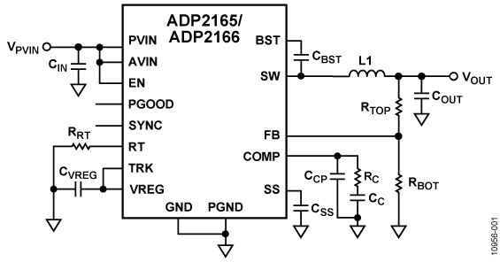
ADP2166-EVALZ
Analog Devices Inc.The ADP2165/ADP2166 are high efficiency, current modecontrol, step-down dc-to-dc regulators with an integrated 19 m?high-side FET and a 15 m? synchronous rectified FET. TheADP2165/ADP2166 combine a small size, 4 mm ? 4 mm LFCSPpackage with an accurate current limit, resulting in a smallerinductor size and a high power density, point of load solution.Key features include precision enable, power-good monitor,and output voltage tracking to facilitate robust sequencing.The switching frequency can be programmed from 250 kHzto 1.4 MHz, or it can be fixed at 620 kHz or 1.2 MHz. Thesynchronization function allows the switching frequency tosynchronize to an external clock, minimizing theelectromagnetic interference (EMI) of the system.The ADP2165/ADP2166 are designed to be extremely flexiblewith the addition of a minimal amount of external componentsto program soft start and control loop compensation.he ADP2165/ADP2166 are supplied from an input voltage of2.7 V to 5.5 V. Output voltage options include 3.3 V, 2.5 V, 1.8 V,1.5 V, 1.2 V, or 1.0 V fixed outputs and adjustable options capableof supporting an output voltage range from 0.6 V to 90% of theinput voltage. Protection features include undervoltage lockout(UVLO), overvoltage protection (OVP), overcurrent protection(OCP), and thermal shutdown (TSD) for robust performance.The ADP2165/ADP2166 operate over the ?40?C to +125?Cjunction temperature range and are available in a 24-leadLFCSP package.Applications Point of load regulation Communications and networking High end consumer Industrial, instrumentation, and healthcare

ADP2323-EVALZ
Analog Devices Inc.The ADP2323 is a full featured, dual output, step-down dc-to-dc regulator based on current-mode architecture. The ADP2323 integrates two high-side power MOSFETs and two low-side drivers for the external N-channel MOSFETs. The two pulse-width mod-ulation (PWM) channels can be configured to deliver dual 3 A outputs or a parallel-to-single 6 A output. The regulator operates from input voltages of 4.5 V to 20 V, and the output voltage can be as low as 0.6 V.The switching frequency can be programmed between 250 kHz and 1.2 MHz, or synchronized to an external clock to minimize interference in multirail applications. The dual PWM channels run 180? out of phase, thereby reducing input current ripple as well as reducing the size of the input capacitor.The bidirectional synchronization pin can be programmed at a 60?, 90?, or 120? phase shift, providing the possibility for a stackable multiphase power solution.The ADP2323 can be set to operate in pulse-frequency modulation (PFM) mode at a light load for higher efficiency or in forced PWM for noise sensitive applications. External compensation and soft start provide design flexibility. Independent enable inputs and power good outputs provide reliable power sequencing. To enhance system reliability, the device also includes undervoltage lockout (UVLO), overvoltage protection (OVP), overcurrent pro-tection (OCP), and thermal shutdown (TSD).The ADP2323 operates over the ?40?C to +125?C junction temperature range and is available in a 32-lead LFCSP_WQ package.APPLICATION Communication infrastructure Networking and servers Industrial and instrumentation Healthcare and medical Intermediate power rail conversion DC-to-dc point of load applications

ADP2381-EVALZ
Analog Devices Inc.The ADP2381 is a current mode control, synchronous, step-down, dc-to-dc regulator. It integrates a 44 m? power MOSFET and a low-side driver to provide a high efficiency solution. The ADP2381 runs from an input voltage of 4.5 V to 20 V and can deliver 6 A of output current. The output voltage can be adjusted to 0.6 V to 90% of the input voltage. The switching frequency of the ADP2381 can be programmed from 250 kHz to 1.4 MHz or fixed at 290 kHz or 550 kHz. The synchronization function allows the switching frequency to be synchronized to an external clock to minimize system noise.External compensation and an adjustable soft start provide design flexibility. The power-good output provides simple and reliable power sequencing. Additional features include programmable undervoltage lockout (UVLO), overvoltage protection (OVP), overcurrent protection (OCP), and thermal shutdown (TSD).The ADP2381 operates over the ?40?C to +125?C junction temperature range and is available in a 16-lead TSSOP_EP package.APPLICATIONS Communication infrastructure Networking and servers Industrial and instrumentation Healthcare and medical Intermediate power rail conversion DC-to-DC point of load application

ADP2384-EVALZ
Analog Devices Inc.The ADP2384 is a synchronous, step-down dc-to-dc regulator with an integrated 44 m?, high-side power MOSFET and an 11.6 m?, synchronous rectifier MOSFET to provide a high efficiency solution in a compact 4 mm ? 4 mm LFCSP package. This device uses a peak current mode, constant frequency pulse-width modulation (PWM) control scheme for excellent stability and transient response. The switching frequency of the ADP2384 can be programmed from 200 kHz to 1.4 MHz. To minimize system noise, the synchronization function allows the switching frequency to be synchronized to an external clock.The ADP2384 requires minimal external components and operates from an input voltage of 4.5 V to 20 V. The output voltage can be adjusted from 0.6 V to 90% of the input voltage and delivers up to 4 A of continuous current. Each IC draws less than 120 ?A current from the input source when it is disabled.This regulator targets high performance applications that require high efficiency and design flexibility. External compensation and an adjustable soft start function provide design flexibility. The power-good output and precision enable input provide simple and reliable power sequencing.Other key features include undervoltage lockout (UVLO), overvoltage protection (OVP), overcurrent protection (OCP), short-circuit protection (SCP), and thermal shutdown (TSD).The ADP2384 operates over the ?40?C to +125?C junction temperature range and is available in a 24-lead, 4 mm ? 4 mm LFCSP package.APPLICATIONS Communications infrastructure Networking and servers Industrial and instrumentation Healthcare and medical Intermediate power rail conversion DC-to-DC point-of-load applications

ADP2386-EVALZ
Analog Devices Inc.The ADP2386 is a synchronous step-down, dc-to-dc regulator with an integrated 44 m?, high-side power MOSFET and an 11 m?, synchronous rectifier MOSFET to provide a high efficiency solution in a compact 4 mm ? 4 mm LFCSP package. This device uses a peak current mode, constant frequency pulse-width modulation (PWM) control scheme for excellent stability and transient response. The switching frequency of the ADP2386 can be programmed between 200 kHz to 1.4 MHz. To minimize system noise, the synchronization function allows the switching frequency to be synchronized to an external clock.The ADP2386 requires minimal external components and operates from an input voltage of 4.5 V to 20 V. The output voltage can be adjusted from 0.6 V to 90% of the input voltage and delivers up to 6 A of continuous current. Each IC draws less than 110 ?A current from the input source when it is disabled.This regulator targets high performance applications that require high efficiency and design flexibility. External compensation and an adjustable soft start function provide design flexibility. The power-good output and precision enable input provide simple and reliable power sequencing.Other key features include undervoltage lockout (UVLO), overvoltage protection (OVP), overcurrent protection (OCP), short-circuit protection (SCP) and thermal shutdown (TSD).The ADP2386 operates over the ?40?C to +125?C junction temperature range and is available in a 24-lead, 4 mm ? 4 mm LFCSP package.Applications Communications infrastructure Networking and servers Industrial and instrumentation Healthcare and medical Intermediate power rail conversion DC-to-dc point-of-load applications

ADP2450ASTZ-3-EVBZ
Analog Devices Inc.The ADP2450 integrates one boost shunt controller with powerdetection, one high efficiency buck regulator, four low offset,low power consumption programmable gain amplifiers (PGAs),one low offset operation amplifier, a fast analog trip circuit, andan actuator driver. The ADP2450 is targeted for low voltagecircuit breakers, such as the molded case circuit breaker(MCCB), and current transformer (CT) powered supplyapplications.The boost output voltage can be up to 36 V and integrates apower detection circuit that prevents the circuit from powerhiccups. The power detection threshold is programmable withresistors.The buck regulator operates over a wide input voltage range of4.5 V to 36 V, and the output voltage can be adjusted down to0.6 V. The buck regulator provides output currents of up to500 mA. The buck regulator works in pulse-width modulation(PWM) mode with a fixed 1.2 MHz switching frequency,providing low output ripple voltage to the system.The output voltage of the buck regulator is monitored by thesupervisory circuit. When the output voltage is below themonitoring threshold, 88% of VFB2 (FB2 regulation voltage), thereset signal is pulled low and can be used to reset themicroprocessor. The monitoring supervisory circuit makes thesystem more reliable.The ADP2450 integrates four low offset, low power consumptionamplifiers. With the programmable gain features, the ADP2450provides accuracy measurement over a wide current input rangebased on the CT turn ratio.A low offset operation amplifier is integrated in the ADP2450for leakage current detection.The ADP2450 also integrates an analog trip circuit, whichprovides fast trip response and enhances system reliability.Additional protection includes buck overcurrent protection(OCP) and system thermal shutdown (TSD).The ADP2450 operates over the ?40?C to +125?C junctiontemperature range and is available either in a 32-lead LFCSP ora 48-lead LQFP packages.Applications Low voltage circuit breaker CT powered supply

ADP2503-EVALZ
Analog Devices Inc.The ADP2503 /?ADP2504 are high efficiency, low quiescent current step-up/step-down dc-to-dc converters that can operate at input voltages greater than, less than, or equal to the regulated output voltage. The power switches and synchronous rectifiers are internal to minimize external part count. At high load currents, the ADP2503 / ADP2504 use a current-mode, fixed frequency pulse-width modulation (PWM) control scheme for optimal stability and transient response. To ensure the longest battery life in portable applications, the ADP2503 / ADP2504 have an optional power save mode that reduces the switching frequency under light load conditions. For wireless and other low noise applications where variable frequency power save mode may cause interference, the logic control input sync forces fixed frequency PWM operation under all load conditions.The ADP2503 / ADP2504 can run from input voltages between 2.3 V and 5.5 V, allowing single lithium or lithium polymer cell, multiple alkaline or NiMH cells, PCMCIA, USB, and other standard power sources. The ADP2503 / ADP2504 have fixed output options, or using the adjustable model, the output voltage can be programmed through an external resistor divider. Compensation is internal to minimize the number of external components.During logic-controlled shutdown, the input is disconnected from the output and draws less than 1 ?A from the input source. Operating as boost converters, the ADP2503 / ADP2504 feature a true load disconnect function that isolates the load from the power source. Other key features include undervoltage lockout to prevent deep battery discharge, and soft start to prevent input current overshoot at startup.APPLICATIONS Wireless handsets Digital cameras/portable audio players Miniature hard disk power supplies USB powered devices
ADP2504CPZ-REDYKIT
Analog Devices Inc.The ADP2503?/ ADP2504 are high efficiency, low quiescent current step-up/step-down dc-to-dc converters that can operate at input voltages greater than, less than, or equal to the regulated output voltage. The power switches and synchronous rectifiers are internal to minimize external device count. At high load currents, the ADP2503 / ADP2504 use a current-mode, fixed frequency pulse-width modulation (PWM) control scheme for optimal stability and transient response. To ensure the longest battery life in portable applications, the ADP2503 / ADP2504 have an optional power save mode that reduces the switching frequency under light load conditions. For wireless and other low noise applications where variable frequency power save mode may cause interference, the logic control input sync forces fixed frequency PWM operation under all load conditions.?The ADP2503 / ADP2504 can run from input voltages between 2.3 V and 5.5 V, allowing single lithium or lithium polymer cell, multiple alkaline or NiMH cells, PCMCIA, USB, and other standard power sources. The ADP2503 / ADP2504 have fixed output options, or using the adjustable model, the output voltage can be programmed through an external resistor divider. Compensation is internal to minimize the number of external components.During logic-controlled shutdown, the input is disconnected from the output and draws less than 1 ?A from the input source. Operating as boost converters, the ADP2503 / ADP2504 feature a true load disconnect function that isolates the load from the power source. Other key features include undervoltage lockout to prevent deep battery discharge, and soft start to prevent input current overshoot at startup.APPLICATIONSWireless handsetsDigital cameras/portable audio playersMiniature hard disk power suppliesUSB powered devices?

ADP5063CP-EVALZ
Analog Devices Inc.The ADP5063 charger is fully compliant with USB 3.0 and the USB Battery Charging 1.2 Compliance Plan Specification, and enables charging via the mini USB VBUS pin from a wall charger, car charger, or USB host port.The ADP5063 operates from a 4 V to 6.7 V input voltage range but is tolerant of voltages up to 20 V, thereby alleviating concerns about USB bus spikes during disconnection or connection scenarios.The ADP5063 features an internal field effect transistor (FET) between the linear charger output and the battery. This permits battery isolation and, therefore, system powering under a dead battery or no battery scenario, which allows immediate system function upon connection to a USB power supply.Based on the type of USB source, which is detected by an external USB detection chip, the ADP5063 can be set to apply the correct current limit for optimal charging and USB compliance.The ADP5063 has three factory-programmable digital input/out-put pins that provide maximum flexibility for different systems. These digital input/output pins permit a combination of features, such as input current limits, charging enable and disable, charging current limits, and a dedicated interrupt output pin.APPLICATIONS Single cell LiFePO4 portable equipment Portable medical devices Portable instrumentation devices Portable consumer devices

ADP5073CP-EVALZ
Analog Devices Inc.The ADP5073 is a high performance dc-to-dc inverting regulator used to generate negative supply rails.The input voltage range of 2.85 V to 15 V supports a wide variety of applications. The integrated main switch enables the generation of an adjustable negative output voltage down to 39 V below the input voltage.The ADP5073 operates at a pin selected 1.2 MHz/2.4 MHz switching frequency. The ADP5073 can synchronize with an external oscillator from 1.0 MHz to 2.6 MHz to ease noise filtering in sensitive applications. The regulator implements programmable slew rate control circuitry for the MOSFET driver stage to reduce electromagnetic interference (EMI).The ADP5073 includes a fixed internal or resistor programmable soft start timer to prevent inrush current at power-up. During shutdown, the regulator completely disconnects the load from the input supply to provide a true shutdown. A power-good pin is available to indicate the output is stable.Other key safety features in the ADP5073 include overcurrent protection (OCP), overvoltage protection (OVP), thermal shutdown (TSD), and input undervoltage lockout (UVLO).The ADP5073 is available in a 16-lead LFCSP and is rated for a ?40?C to +125?C operating junction temperature range.Applications Bipolar amplifiers, ADCs, digital-to-analog converters (DACs), and multiplexers High speed converters Radio frequency (RF) power amplifier (PA) bias Optical modules

ADP5074CP-EVALZ
Analog Devices Inc.The ADP5074 is a high performance dc-to-dc inverting regulator used to generate negative supply rails.The input voltage range of 2.85 V to 15 V supports a wide variety of applications. The integrated main switch enables the generation of an adjustable negative output voltage down to 39 V below the input voltage.The ADP5074 operates at a pin selected 1.2 MHz/2.4 MHz switching frequency. The ADP5074 can synchronize with an external oscillator from 1.0 MHz to 2.6 MHz to ease noise filtering in sensitive applications. The regulator implements programmable slew rate control circuitry for the MOSFET driver stage to reduce electromagnetic interference (EMI).The ADP5074 includes a fixed internal or resistor programmable soft start timer to prevent inrush current at power-up. During shutdown, the regulator completely disconnects the load from the input supply to provide a true shutdown. A power good pin is available to indicate the output is stable.Other key safety features in the ADP5074 include overcurrent protection (OCP), overvoltage protection (OVP), thermal shutdown (TSD), and input undervoltage lockout (UVLO).The ADP5074 is available in a 16-lead LFCSP and is rated for a ?40?C to +125?C operating junction temperature range.Applications Bipolar amplifiers, ADCs, digital-to-analog converters (DACs), and multiplexers High speed converters Radio frequency (RF) power amplifier (PA) bias Optical modules

ADP5133CB-EVALZ
Analog Devices Inc.The ADP5133 combines two high performance buck regulators in a tiny, 16-ball, 2 mm ? 2 mm WLCSP to meet demanding performance and board space requirements.The high switching frequency of the buck regulators enables tiny multilayer external components and minimizes the board space. When the MODE pin is set high, the buck regulators operate in forced PWM mode. When the MODE pin is set low and the buck regulators operate in PWM mode, the load current is above a predefined threshold. When the load current falls below a predefined threshold, the regulators operate in power save mode (PSM), improving the light load efficiency.The two bucks operate out of phase to reduce the input capacitor requirement and noise.The regulators in the ADP5133 are activated through dedicated enable pins. The output voltages can be externally set through a resistor feedback network.Applications Power for processors, ASICs, FPGAs, and RF chipsets Portable instrumentation and medical devices Space constrained devices

ADP5360CB-EVALZ
Analog Devices Inc.The ADP5360 combines one high performance linear charger?for a single lithium-ion (Li-Ion)/lithium-polymer (Li-Poly)?battery with a programmable, ultralow quiescent current fuel?gauge and battery protection circuit, one ultralow quiescent?buck, one buck boost switching regulator, and a supervisory?circuit that can monitor output voltage.The ADP5360 charger operates at up to 6.8 V to prevent USB?bus spiking during disconnect or connect scenarios.The ADP5360 features an internal isolation field effect transistor?(FET) between the linear charger output and the battery node.?The full battery protection features are activated when the device is?in the battery overcharge and overdischarge fault conditions.The ADP5360 fuel gauge uses a voltage-based algorithm with?an adaptive filter limitation solution. The fuel gauge reports?real-time battery state of charge (SOC) for the rechargeable?Li-Ion battery with ultralow quiescent current.The ADP5360 buck regulator operates at 1.0 MHz switching?frequency in forced pulse-width modulation (FPWM) mode.?In hysteresis mode, the regulator achieves excellent efficiency at?a low output power.The ADP5360 buck boost regulator only operates in hysteresis?mode and outputs a voltage less than or greater than the battery?voltage.The ADP5360 supervisory circuits monitor the regulator output?voltage and provide a power-on reset signal to the system. A?watchdog timer and an external pushbutton can reset the?microprocessor.The I2C-compatible interface enables the programmability of all?battery charging parameters, the protection threshold, the buck?output voltage, and the status bit readback.The ADP5360 operates over the ?40?C to +85?C junction?temperature range and is available in a 32-ball, 2.56 mm נ2.56 mm wafer level chip scale package (WLCSP).Applications Rechargeable Li-Ion/Li-Poly battery-powered devices Portable consumer devices Portable medical devices Wearable devices


