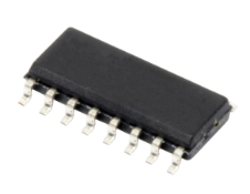
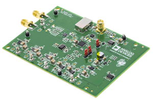
ADL5562-EVALZ
Analog Devices Inc.The ADL5562 is a high performance differential amplifier optimized for RF and IF applications. The amplifier offers low noise of 2.1 nV/?Hz and excellent distortion performance over a wide frequency range, making it an ideal driver for high speed 8-bit to 16-bit ADCs.The ADL5562 provides three gain levels of 6 dB, 12 dB, and 15.5 dB through a pin-strappable configuration. For the single-ended input configuration, the gains are reduced to 5.6 dB, 11.1 dB, and 14.1 dB. Using an external series input resistor expands the amplifier gain flexibility and allows for any gain selection from 0 dB to 15.5 dB.The quiescent current of the ADL5562 is typically 80 mA and, when disabled, consumes less than 3 mA, offering excellent input-to-output isolation.The device is optimized for wideband, low distortion performance. These attributes, together with its adjustable gain capability, make this device the amplifier of choice for general-purpose IF and broadband applications where low distortion, noise, and power are critical. This device is optimized for the best combination of slew speed, bandwidth, and broadband distortion. These attributes allow it to drive a wide variety of ADCs and make it ideally suited for driving mixers, pin diode attenuators, SAW filters, and multielement discrete devices.Fabricated on an Analog Devices, Inc., high speed SiGe process, the ADL5562 is supplied in a compact 3 mm ? 3 mm, 16-lead LFCSP package and operates over the temperature range of ?40?C to + 85?C.APPLICATIONS Differential ADC drivers Single-ended to differential conversion RF/IF gain blocks SAW filter interfacing
ADL5604-EVALZ
Analog Devices Inc.The ADL5604 is a very broadband RF driver amplifier that operates over the wide frequency range of 700 MHz to 2700 MHz. The ADL5604 is also highly linear and has a very low power consumption, enabling the driver to be packaged in a compact 16-lead, 4 mm ? 4 mm LFCSP.For thermal management, the ADL5604 uses an exposed paddle, and the upper and lower pins of the package are all grounded, which gives the ADL5604 excellent thermal transfer characteristics.The ADL5604 can be quickly powered down or up in 50 ns for applications requiring TX shutdown, such as TDD systems.The ADL5604 operates on a single 5 V supply voltage and draws only 318 mA of supply current.The driver is fabricated on a GaAs HBT process and operates from ?40?C to +85?C. A fully populated evaluation board is available.
ADL5725-EVALZ
Analog Devices Inc.The ADL5725 is a narrow-band, high performance, low noise amplifier (LNA) targeting microwave radio link receiver designs. The monolithic silicon germanium (SiGe) design is optimized for microwave radio link bands ranging from 17.7 GHz to 19.7 GHz. The unique design offers a single-ended 50 ? input impedance and provides a 100 ? balanced differential output that is ideal for driving Analog Devices, Inc., differential downconverters and radio frequency (RF) sampling analog-to-digital converters (ADCs). This low noise amplifier provides noise figure performance that, in the past, required more expensive three-five (III-V) compounds process technology to achieve.The ADL5721 and ADL5723 to ADL5726 family of narrow-band LNAs are each packaged in a tiny, thermally enhanced, 2.00 mm ? 2 mm LFCSP package. The ADL5721 and ADL5723 to ADL5726 family operates over the temperature range of ?40?C to +85?C.Applications Point to point microwave radios Instrumentation Satellite communications (SATCOM) Phased arrays
ADL5802-EVALZ
Analog Devices Inc.The ADL5802 uses high linearity, double-balanced, active mixer cores with integrated LO buffer amplifiers to provide high dynamic range frequency conversion from 100 MHz to 6 GHz. The mixers benefit from a proprietary linearization architecture that provides enhanced input IP3 performance when subject to high input levels. A bias adjust feature allows the input linearity, SSB noise figure, and dc current to be optimized using a single control pin. The high input linearity allows the device to be used in demanding cellular applications where in-band blocking signals may otherwise result in degradation in dynamic performance. The balanced active mixer arrangement provides superb LO to RF and LO to IF leakage, typically better than ?30 dBm.The IF outputs are designed for a 200 ? source impedance and provide a typical voltage conversion gain of 7.6 dB when loaded into a 200 ? load.The ADL5802 is fabricated using a SiGe high performance IC process. The device is available in a compact 4 mm ? 4 mm, 24-lead LFCSP package and operates over a ?40?C to +85?C temperature range. An evaluation board is also available.APPLICATIONSCellular base station receiversMain and diversity receiver designsRadio link downconvertersData Sheet, Rev 0, 11/2009
ADL5902-EVALZ
Analog Devices Inc.The ADL5902 is a true rms responding power detector that hasa 65 dB measurement range when driven with a single-ended 50 ? source. This feature makes the ADL5902 frequencyversatile by eliminating the need for a balun or any other form of external input tuning for operation up to 9 GHz.The ADL5902 provides a solution in a variety of high frequencysystems requiring an accurate measurement of signal power. Requiring only a single supply of 5 V and a few capacitors, it is easy to use and capable of being driven single-ended or with abalun for differential input drive. The ADL5902 can operate from 50 MHz to 9 GHz and can accept inputs from ?62 dBm to at least +3 dBm with large crest factors, such as GSM, CDMA,W-CDMA, TD-SCDMA, WiMAX, and LTE modulated signals.The ADL5902 can determine the true power of a high frequency signal having a complex low frequency modulation envelope or can be used as a simple low frequency rmsvoltmeter. Used as a power measurement device, VOUT isconnected to VSET. The output is then proportional to thelogarithm of the rms value of the input. In other words, thereading is presented directly in decibels and is scaled 1.06 V per decade, or 53 mV/dB; other slopes are easily arranged. In controller mode, the voltage applied to VSET determines thepower level required at the input to null the deviation from the set point. The output buffer can provide high load currents.The ADL5902 has 1.5 mW power consumption when powereddown by a logic high applied to the PWDN pin. It powers up within approximately 5 ?s to its nominal operating current of 73 mA at 25?C. The ADL5902 is supplied in a 4 mm ? 4 mm,16-lead LFCSP for operation over the wide temperature rangeof ?40?C to +125?C.The ADL5902 is also pin-compatible with the AD8363, 50 dBdynamic range TruPwr? detector. This feature allows the designer to create one circuit layout for projects requiring different dynamic ranges. A fully populated RoHS-compliant evaluation board is available.Applications Power amplifier linearization/control loops Transmitter power controls Transmitter signal strength indication (TSSI) RF instrumentation
ADL5906-EVALZ
Analog Devices Inc.The ADL5906 is a true rms responding power detector that has a 67 dB measurement range when driven with a single-ended 50 ? source. The easy to use input makes the ADL5906 frequency versatile by eliminating the need for a balun or any other form of external input tuning for operation up to 10 GHz.The ADL5906 provides a solution in a variety of high frequency systems requiring an accurate rms measurement of signal power. The ADL5906 can operate from 10 MHz to 10 GHz and can accept inputs from ?65 dBm to +8 dBm with varying crest factors and bandwidths, such as GSM-EDGE, CDMA, W-CDMA,TD-SCDMA, WiMAX, and OFDM-based LTE carriers. In addition, its temperature stability over the broad temperature range of ?55?C to +125?C makes it ideally suited for a wide array of communications, military, industrial, and instrumentation applications.Used as a power measurement device, VRMS is connected to VSET. The output is then proportional to the logarithm of the rms value of the input. In other words, the reading is presented directly in decibels and is scaled 1.1 V per decade, or 55 mV/dB; other slopes are easily arranged. In controller mode, the voltage applied to VSET determines the power level required at the input to null the deviation from the setpoint. The output buffer can provide high load currents.Requiring only a single supply of 5 V and a few capacitors, it is easy to use and capable of being driven single-ended or with a balun for differential input drive. The ADL5906 has a low 250 ?A sleep current when powered down by a logic high applied to the PWDN pin. It powers up within approximately 1.4 ?s to its nominal operating current of 68 mA at 25?C.The ADL5906 is supplied in a 4 mm ? 4 mm, 16-lead LFCSP and it is pin compatible with the ADL5902 and the AD8363 TruPwr? rms detectors. This feature allows the designer to create one circuit layout for projects requiring different dynamic ranges. A fully populated RoHS-compliant evaluation board is available.Applications Power amplifier linearization/control loops Transmitter signal strength indication (TSSI) RF instrumentation
ADL5960-EVALZ
Analog Devices Inc.The ADL5960 is a wideband vector network analyzer front-end consisting of a resistive bidirectional bridge, down-conversion mixers, programmable IF amplifiers and filters, and a highly flexible local oscillator (LO) interface. The bridge provides >10 dB of directivity up to 17 GHz, and the primary transmission line of the bridge, from RFIN to RFOUT, is wideband impedance matched to 50 ? and has a flat frequency response with The ADL5960 supports several different LO interface configurations that simplify the clocking design of a VNA solution as well as the interfacing of the device to an analog-to-digital converter (ADC). The frequency divider and multipliers in the LO interface enable measurement sweeps beyond the operating frequency range of the source driving the (LOP and LOM) pins. This enables operation over the full 20 GHz bandwidth of the ADL5960 using a 6 GHz synthesizer as the LO source. The IF frequency offset mixer, driven through the (OFP and OFM) interface, enables further simplification by allowing the (swept) RF and LO signals to be driven by the same frequency source. The frequency of the IF output signals is then determined by the low-frequency source driving the (OFP and OFM) interface. Driving this interface at the ADC sample frequency with the divide by 4 enabled, automatically centers the IF output signal in the first Nyquist zone.The IF filters with programmable bandwidth and IF amplifiers with individually programmable gain enable simultaneous dynamic range optimization of the IF signals at the incident channel (IFFP and IFFM) and reverse channel (IFRP and IFRM) IF interfaces. The IF amplifiers have an adjustable output common-mode level and sufficient drive capability to interface directly with a wide range of ADCs.All configurations and functions in the ADL5960 are fully programmable through a 3-wire serial peripheral interface (SPI) using the ADI-SPI interface standard. The ADL5960 is offered in a small footprint 26-lead, 3 mm ? 4 mm LFCSP.APPLICATIONSBroadband, multi-port vector network analyzersS-parameter magnitude and phase measurementIn-line RF power measurementAutomated test equipmentReflectometersMaterials analysis
ADL6316-EVALZ
Analog Devices Inc.The ADL6316 is a transmit variable gain amplifier (VGA) that?provides an interface from radio frequency digital-to-analog?converters (RF DACs), transceivers, and systems on a chip (SoC)?to power amplifiers. Integrated balun and hybrid couplers allow?high performance RF capability in the frequency range of?500 MHz to 1000 MHz.To optimize performance vs. power level, the ADL6316 includes?a voltage variable attenuator (VVA), high linearity amplifiers,?and a digital step attenuator (DSA). All of the devices integrated?into the ADL6316 are programmable via a 4-wire serial port?interface (SPI).The ADL6316 is manufactured on an advanced silicon germanium?(SiGe), bipolar complementary metal-oxide semiconductor?(BiCMOS) process.Applications 2G/3G/4G/long-term evolution (LTE) in FDD/TDD broadband?communication systems
ADM1270CP-EVALZ
Analog Devices Inc.The ADM1270 is a current-limiting controller that providesinrush current limiting and overcurrent protection for modularor battery-powered systems. When circuit boards are insertedinto a live backplane, discharged supply bypass capacitors drawlarge transient currents from the backplane power bus as theycharge. These transient currents can cause permanent damageto connector pins, as well as dips on the backplane supply thatcan reset other boards in the system.The ADM1270 is designed to control the inrush current, whenpowering on the system, via an external P-channel field effecttransistor (FET).To protect the system from a reverse polarity input supply, thereis a provision made to control an additional external P-channelFET. This feature prevents reverse current flow in case of a reversepolarity connection, which can damage the load or the ADM1270.The ADM1270 is available in a 3 mm ? 3 mm, 16-lead LFCSP anda 16-lead QSOP. Applications Industrial modules Battery-powered/portable instrumentation
ADM7154RD-1.8EVALZ
Analog Devices Inc.TThe ADM7154 is a linear regulator that operates from 2.3 V to5.5 V and provides up to 600 mA of load current. Using anadvanced proprietary architecture, it provides high powersupply rejection and ultralow noise, achieving excellent line andload transient response with only a 10 ?F ceramic output capacitor.There are 16 standard output voltages for the ADM7154. Thefollowing voltages are available in stock: 1.2 V, 1.8 V, 2.5 V, 2.8 V,3.0 V, and 3.3 V. Additional voltages are available by specialorder: 1.3 V, 1.5 V, 1.6 V, 2.0 V, 2.2 V, 2.6 V, 2.7 V, 2.9 V, 3.1 V,and 3.2 V.The ADM7154 regulator typical output noise is 0.9 ?V rms from100 Hz to 100 kHz for fixed output voltage options and1.5 nV/?Hz for noise spectral density from 10 kHz to 1 MHz. The ADM7154 is available in 8-lead, 3 mm ? 3 mm LFCSP and8-lead SOIC packages, making it not only a very compactsolution, but also providing excellent thermal performance forapplications requiring up to 600 mA of load current in a small,low profile footprint.Applications Regulation to noise sensitive applications: PLLs, VCOs, and PLLs with integrated VCOs Communications and infrastructure Backhaul and microwave links
ADM7170CP-EVALZ
Analog Devices Inc.The ADM7170 is a CMOS, low dropout linear regulator (LDO) that operates from 2.3 V to 6.5 V and provides up to 500 mA of output current. This high output current LDO is ideal for regulation of high performance analog and mixed signal circuits operating from 6 V down to 1.2 V rails. Using an advanced proprietary architecture, the device provides high power supply rejection and low noise, and achieves excellent line and load transient response with just a small 4.7 ?F ceramic output capacitor. Load transient response is typically 1.5 ?s for a 1 mA to 500 mA load step.The ADM7170 is available in 17 fixed output voltage options. The following voltages are available from stock: 1.3 V, 1.8 V, 2.5 V, 3.0 V, 3.3 V, 4.2 V, and 5.0 V. Additional voltages that are available by special order are: 1.5 V, 1.85 V, 2.0 V, 2.2 V, 2.7 V, 2.75 V, 2.8 V, 2.85 V, 3.8 V, and 4.6 V. An adjustable version is also available that allows output voltages that range from 1.2 V to VIN ? VDO with an external feedback divider.Inrush current can be controlled by adjusting the start-up time via the soft start pin. The typical start-up time with a 1 nF soft start capacitor is about 1.0 ms.The ADM7170 regulator output noise is 5 ?V rms independent of the output voltage. The ADM7170 is available in an 8-lead, 3 mm ? 3 mm LFCSP, making it not only a very compact solution, but also providing excellent thermal performance for applications requiring up to 500 mA of output current in a small, low profile footprint.Applications Regulation to noise sensitive applications: ADC and DAC circuits, precision amplifiers, PLLs/VCOs, and clocking ICs Communications and infrastructure Medical and healthcare Industrial and instrumentation
ADM7171CP-EVALZ
Analog Devices Inc.The ADM7171 is a CMOS, low dropout linear regulator (LDO) that operates from 2.3 V to 6.5 V and provides up to 1 A of output current. This high output current LDO is ideal for regulation of high performance analog and mixed signal circuits operating from 6 V down to 1.2 V rails. Using an advanced proprietary architecture, the device provides high power supply rejection and low noise, and achieves excellent line and load transient response with just a small 4.7 ?F ceramic output capacitor. Load transient response is typically 1.5 ?s for a 1 mA to 500 mA load step.The ADM7171 is available in 17 fixed output voltage options. The following voltages are available from stock: 1.3 V, 1.8 V, 2.5 V, 3.0 V, 3.3 V, 4.2 V, and 5.0 V. Additional voltages that are available by special order are: 1.5 V, 1.85 V, 2.0 V, 2.2 V, 2.7 V, 2.75 V, 2.8 V, 2.85 V, 3.8 V, and 4.6 V. An adjustable version is also available that allows output voltages that range from 1.2 V to VIN ? VDO with an external feedback divider.Inrush current can be controlled by adjusting the start-up time via the soft start pin. The typical start-up time with a 1 nF soft start capacitor is 1.0 ms.The ADM7171 regulator output noise is 5 ?V rms independent of the output voltage. The ADM7171 is available in an 8-lead, 3 mm ? 3 mm LFCSP, making it not only a very compact solution, but also providing excellent thermal performance for applications requiring up to 1 A of output current in a small, low profile footprint.Applications Regulation to noise sensitive applications: ADC and DAC circuits, precision amplifiers, PLLs/VCOs, and clocking ICs Communications and infrastructure Medical and healthcare Industrial and instrumentation
ADM8613-EVALZ
Analog Devices Inc.The ADM8611/ADM8612/ADM8613/ADM8614/ADM8615?are voltage supervisory circuits that monitor power supply voltage levels and code execution integrity in microprocessor-based systems. Apart from providing power-on reset signals, an on-chip watchdog timer can reset the microprocessor if it fails to strobe within a preset timeout period. A reset signal can also be asserted by an external push-button through a manual reset input.The ultralow power consumption of these devices makes them suitable for power efficiency sensitive systems, such as battery-powered portable devices and energy meters.The features of each member of the device family are shown in Table 9 in the data sheet. Each device subdivides into submodels with differences in factory preset voltage monitoring threshold options. In the range of 2 V to 4.63 V, 10 options are available for the ADM8611. In the range of 2.32 V to 4.63 V, five options are available for both the ADM8613 and ADM8614. A separate supply input allows the ADM8612 and ADM8615 to monitor 20 different low voltage levels from 0.5 V to 1.9 V. Not all device options are available as standard models.The ADM8611, ADM8612, ADM8613, and ADM8615 can reset on demand through the manual reset input. The watchdog function on the ADM8613, ADM8614, and ADM8615 monitors the heartbeat of the microprocessor through the WDI pin. The ADM8613 and ADM8614 have a watchdog disable input, which allows the user to disable the watchdog function, if required. The ADM8614 also has a watchdog timeout extension input, allowing the watchdog timeout to be extended from 1.6 sec to 100 sec.The ADM8611/ADM8612/ADM8613/ADM8614/ADM8615 are available in a 6-ball, 1.46 mm ? 0.96 mm WLCSP. These devices are specified over the temperature range of ?40?C to +85?C.??Applications Portable/battery-operated equipment Microprocessor systems Energy metering Energy harvesting
ADMV1010-EVALZ
Analog Devices Inc.The ADMV1010 is a compact, gallium arsenide (GaAs) design, monolithic microwave integrated circuit (MMIC), I/Q downconverter in a RoHS compliant package optimized for point to point microwave radio designs that operates in the 12.6 GHz to 15.4 GHz frequency range. The ADMV1010 is optimized to work as a low noise, upper sideband (low side local oscillator (LO)), image reject downconverter.The ADMV1010 provides 15 dB of conversion gain with 25 dB of image rejection. The ADMV1010 uses a radio frequency (RF), low noise amplifier (LNA) followed by an in-phase/quadrature (I/Q) double balanced mixer, where a driver amplifier drives the LO. IF1 and IF2 mixer outputs are provided, and an external 90? hybrid is needed to select the required sideband. The I/Q mixer topology reduces the need for filtering the unwanted sideband. The ADMV1010 is a much smaller alternative to hybrid style SSB downconverter assemblies, and it eliminates the need for wire bonding by allowing the use of surface-mount manufacturing assemblies.The ADMV1010 downconverter comes in a compact, thermally enhanced, 4.9 mm ? 4.9 mm, 32-terminal LCC package. The ADMV1010 operates over the ?40?C to +85?C temperature range.Applications Point to point microwave radios Radars and electronic warfare systems Instrumentation and automatic test equipment Satellite communications
ADMV1011-EVALZ
Analog Devices Inc.The ADMV1011 is a compact, gallium arsenide (GaAs) design,monolithic microwave integrated circuit (MMIC), doublesideband (DSB) upconverter in a RoHS compliant packageoptimized for point to point microwave radio designs thatoperates in the 17 GHz to 24 GHz frequency range.The ADMV1011 provides 21 dB of conversion gain with 32 dBcof sideband rejection for the lower sideband and 23 dBc ofsideband rejection for the upper sideband. The ADMV1011uses a radio frequency (RF) amplifier preceded by an inphase/quadrature (I/Q) double balanced mixer, where a driveramplifier drives the local oscillator (LO) with a 2? multiplier.IF1 and IF2 mixer inputs are provided and an external 90?hybrid is needed to select the required sideband. The I/Q mixertopology reduces the need for filtering the unwanted sideband.The ADMV1011 is a much smaller alternative to hybrid styleDSB upconverter assemblies and it eliminates the need for wirebonding by allowing the use of surface-mount manufacturingassemblies.The ADMV1011 upconverter comes in a compact, thermallyenhanced, 4.9 mm ? 4.9 mm LCC package. The ADMV1011operates over the ?40?C to +85?C temperature range.Applications Point to point microwave radios Radars and electronic warfare systems Instrumentation, automatic test equipment
ADMV1013-EVALZ
Analog Devices Inc.The ADMV1013 is a wideband, microwave upconverter optimized for point to point microwave radio designs operating in the 24 GHz to 44 GHz radio frequency (RF) range.The upconverter offers two modes of frequency translation. The device is capable of direct conversion to RF from baseband in-phase quadrature (I/Q) input signals, as well as single-sideband (SSB) upconversion from complex intermediate frequency (IF) inputs. The baseband I/Q input path can be disabled and modulated complex IF signals, anywhere from 0.8 GHz to 6.0 GHz, can be inserted in the IF path and upconverted to 24 GHz to 44 GHz while suppressing the unwanted sideband by typically better than 26 dBc. The serial port interface (SPI) allows adjustment of the quadrature phase and mixer gate voltage to allow optimum sideband suppression and local oscillator (LO) nulling. In addition, the SPI interface allows powering down the output envelope detector to reduce power consumption.The ADMV1013 upconverter comes in a 40-terminal land grid array package (LGA) package. The ADMV1013 operates over the ?40?C to +85?C case temperature range.Applications Point to point microwave radios Radar, electronic warfare systems Instrumentation, automatic test equipment (ATE)
ADMV1139IQ-EVALZ
Analog Devices Inc.The ADMV1139 is an silicon on isolator (SOI), microwave, upconverter and downconverter optimized for 5G radio designs operating in the 37 GHz to 48.2 GHz frequency range.Both upconverters and downconverters offer two modes of frequency translation. One mode is conversion from and/or to complex intermediate frequency (IF) signals, which then pass through an on-chip 90? IF hybrid, known as IF mode.The other mode is a direct conversion from and/or to single-ended or differential baseband inphase/quadrature (I/Q) inputs and outputs, known as baseband mode. The I/Q baseband output common-mode voltage is programmable between 0 V and 1.5 V. The SPI provides fine adjustment of the quadrature phase to optimize I/Q demodulation performance.When the device is used as an image rejecting downconverter, the unwanted image term is typically rejected to 26 dBc, before calibration. The ADMV1139 offers a square law power detector to allow monitoring of the power levels at the mixer inputs of the downconverter.The RF receive input, RF transmit output, and local oscillator (LO) interface are all single-ended and matched to 50 ?. The on-chip RF switch provides the option to combine the transmit and receive RF ports together for time division duplex (TDD) applications.The serial port interface (SPI) provides adjustment of the quadrature phase to allow optimum sideband rejection. In addition, the SPI allows powering down the output envelope detector to reduce power consumption when carrier feedthrough optimization is not necessary.The ADMV1139 upconverter and downconverter is housed in a compact, thermally enhanced, 6 mm ? 6.5 mm, ball grid array (BGA) package. This BGA package enables the ability to heat sink the ADMV1139 from the top of the package for the most efficient thermal heat sinking. The ADMV1139 operates over the ?40?C to +95?C TC range.APPLICATIONSMillimeter-wave 5G applicationsPoint to point microwave radiosRadar and electronic warfare systemsInstrumentation and automatic test equipment (ATE)
ADMV1550-EVALZ
Analog Devices Inc.The ADMV1550 is a general-purpose, double balanced mixer in a leadless, RoHS compliant, surface-mount technology (SMT) package that can be used as an upconverter or down-converter between 15 GHz and 67 GHz. The wide bandwidth from 0 GHz to 20 GHz on the intermediate frequency (IF) port allows flexible frequency planning to avoid spurious products. This mixer is fabricated in a gallium arsenide (GaAs), monolithic microwave integrated circuit (MMIC) process and requires no external components or matching circuitry. The ADMV1550 provides excellent local oscillator (LO) to radio frequency (RF) and LO to IF suppression due to optimized balun structures. The mixer operates with an LO amplitude above 15 dBm. The RoHS compliant ADMV1550 eliminates the need for wire bonding, allowing the use of surface-mount manufacturing techniques.APPLICATIONSMicrowave and very small aperture terminal (VSAT) radiosTest equipmentMilitary electronic warfare (EW)Electronic countermeasure (ECM)Command, control, communications, and intelligence (C3I)
ADMV4420-EVALZ
Analog Devices Inc.The ADMV4420 is a highly integrated, double balanced, active mixer with an integrated fractional-N synthesizer, ideally suited for next generation K band satellite communications.The RF front end consists of an integrated RF balun and low noise amplifier (LNA) for an optimal, 7 dB, single-sideband noise figure while minimizing external components. Additionally, the high dynamic range IF output amplifier provides a nominal conversion gain of 36 dB.An integrated low phase noise, fractional-N, phase-locked loop (PLL) with a multicore voltage controlled oscillator (VCO) and internal 2? multiplier generate the necessary on-chip LO signal for the double balanced mixer, eliminating the need for external frequency synthesis. The multicore VCO uses an internal autocalibration routine that allows the PLL to select the necessary settings and lock in approximately 400 ?s.The reference input to the PLL employs a differentially excited 50 MHz crystal oscillator. Alternatively, the reference input can be driven by an external, singled-ended, 50 MHz source. The phase frequency detector (PFD) comparison frequency of the PLL operates up to 50 MHz.The ADMV4420 is fabricated on a silicon germanium (SiGe), bipolar complementary metal-oxide semiconductor (BiCMOS) process, and is available in a 32-lead, RoHS compliant, 5 mm ? 5 mm LFCSP package with an exposed pad. The device is specified over the ?40?C to +85?C temperature range on a 5 V power supply.Applications Satellite communication Point to point microwave communication


