
AD9234-500EBZ
Analog Devices Inc.The AD9234 is a dual, 12-bit, 1 GSPS/500 MSPS ADC. The device has an on-chip buffer and sample-and-hold circuit designed for low power, small size, and ease of use. This product is designed for sampling wide bandwidth analog signals. The AD9234 is optimized for wide input bandwidth, high sampling rate, excellent linearity, and low power in a small package.The dual ADC cores feature a multistage, differential pipelined architecture with integrated output error correction logic. Each ADC features wide bandwidth buffered inputs supporting a variety of user-selectable input ranges. An integrated voltage reference eases design considerations. Each ADC data output is internally connected to an optional decimate-by-2 block. The AD9234 has several functions that simplify the automatic gain control (AGC) function in a communications receiver.?The programmable threshold detector allows monitoring of the incoming signal power using the fast detect output bits of the ADC. If the input signal level exceeds the programmable threshold, the fast detect indicator goes high. Because this threshold indicator has low latency, the user can quickly turn down the system gain to avoid an overrange condition at the ADC input. In addition to the fast detect outputs, the AD9234 also offers signal monitoring capability. The signal monitoring block provides additional information about the signal being digitized by the ADC.Users can configure the Subclass 1 JESD204B-based high speed serialized output in a variety of one-, two-, or four-lane configurations, depending on the acceptable lane rate of the receiving logic device and the sampling rate of the ADC. Multiple device synchronization is supported through the SYSREF? and SYNCINB? input pins.The AD9234 has flexible power-down options that allow significant power savings when desired. All of these features can be programmed using a 1.8 V to 3.3 V capable 3-wire SPI.The AD9234 is available in a Pb-free, 64-lead LFCSP and is specified over the ?40?C to +85?C industrial temperature range. This product is protected by a U.S. patent.Product Highlights Low power consumption analog core, 12-bit, 1.0 GSPS dual analog-to-digital converter (ADC) with 1.5 W per channel. Wide full power bandwidth supports IF sampling of signals up to 2 GHz. Buffered inputs with programmable input termination eases filter design and implementation. Flexible serial port interface (SPI) controls various product features and functions to meet specific system requirements. Programmable fast overrange detection. 9 mm ? 9 mm 64-lead LFCSP. Pin compatible with the AD9680 14-bit, 1 GSPS dual ADC.Applications Communications Diversity multiband, multimode digital receivers 3G/4G, TD-SCDMA, W-CDMA, GSM, LTE Point-to-point radio systems Digital predistortion observation path General-purpose software radios Ultrawideband satellite receiver Instrumentation (spectrum analyzers, network analyzers, integrated RF test solutions) Digital oscilloscopes High speed data acquisition systems DOCSIS 3.0 CMTS upstream receive paths HFC digital reverse path receivers

AD9257-65EBZ
Analog Devices Inc.The AD9257 is an octal, 14-bit, 40 MSPS and 65 MSPS analog-to-digital converter (ADC) with an on-chip sample-and-hold circuit designed for low cost, low power, small size, and ease of use. The product operates at a conversion rate of up to 65 MSPS and is optimized for outstanding dynamic performance and low power in applications where a small package size is critical.The ADC requires a single 1.8 V power supply and LVPECL-/ CMOS-/LVDS-compatible sample rate clock for full performance operation. No external reference or driver components are required for many applications.The ADC automatically multiplies the sample rate clock for the appropriate LVDS serial data rate. A data clock output (DCO) for capturing data on the output and a frame clock output (FCO) for signaling a new output byte are provided. Individual channel power-down is supported and typically consumes less than 2 mW when all channels are disabled.The ADC contains several features designed to maximize flexibility and minimize system cost, such as programmable clock and data alignment and programmable digital test pattern generation. The available digital test patterns include built-in deterministic and pseudorandom patterns, along with custom user-defined test patterns entered via the serial port interface (SPI).The AD9257 is available in an RoHS-compliant, 64-lead LFCSP. It is specified over the industrial temperature range of ?40?C to +85?C. This product is protected by a U.S. patent. APPLICATIONS Medical imaging and nondestructive ultrasound Portable ultrasound and digital beam-forming systems Quadrature radio receivers Diversity radio receivers Optical networking Test EquipmentPRODUCT HIGHLIGHTS Small Footprint. Eight ADCs are contained in a small, space-saving package. Low Power of 55 mW/Channel at 65 MSPS with Scalable Power Options. Ease of Use. A data clock output (DCO) is provided that operates at frequencies of up to 455 MHz and supports double data rate (DDR) operation. User Flexibility. The SPI control offers a wide range of flexible features to meet specific system requirements. Pin Compatible with the AD9637 (12-Bit Octal ADC).

AD9266-80EBZ
Analog Devices Inc.The AD9266 is a monolithic, single-channel 1.8 V supply,16-bit, 20 MSPS/40 MSPS/65 MSPS/80 MSPS analog-to-digitalconverter (ADC). It features a high performance sample-and-holdcircuit and on-chip voltage reference.The product uses multistage differential pipeline architecturewith output error correction logic to provide 16-bit accuracy at80 MSPS data rates and to guarantee no missing codes over thefull operating temperature range.The ADC contains several features designed to maximizeflexibility and minimize system cost, such as programmableclock and data alignment and programmable digital test patterngeneration. The available digital test patterns include built-indeterministic and pseudorandom patterns, along with customuser-defined test patterns entered via the serial port interface (SPI).A differential clock input with a selectable internal 1-to-8 divideratio controls all internal conversion cycles. An optional duty cyclestabilizer (DCS) compensates for wide variations in the clock dutycycle while maintaining excellent overall ADC performance.The interleaved digital output data is presented in offset binary,gray code, or twos complement format. A DCO is provided toensure proper latch timing with receiving logic. Both 1.8 V and3.3 V CMOS levels are supported.The AD9266 is available in a 32-lead RoHS-compliant LFCSPand is specified over the industrial temperature range (?40?Cto +85?C).Product Highlights The AD9266 operates from a single 1.8 V analog power supply and features a separate digital output driver supply to accommodate 1.8 V to 3.3 V logic families. The sample-and-hold circuit maintains excellent performance for input frequencies up to 200 MHz and is designed for low cost, low power, and ease of use. A standard serial port interface supports various product features and functions, such as data output formatting, internal clock divider, power-down, DCO and data output (D15_D14 to D1_D0) timing and offset adjustments, and voltage reference modes. The AD9266 is packaged in a 32-lead RoHS-compliant LFCSP that is pin compatible with the AD9609 10-bit ADC, the AD9629 12-bit ADC, and the AD9649 14-bit ADC, enabling a simple migration path between 10-bit and 16-bit converters sampling from 20 MSPS to 80 MSPS.Applications Communications Diversity radio systems Multimode digital receivers GSM, EDGE, W-CDMA, LTE, CDMA2000, WiMAX, TD-SCDMA Smart antenna systems Battery-powered instruments Handheld scope meters Portable medical imaging Ultrasound Radar/LIDAR PET/SPECT imaging

AD9510/PCBZ
Analog Devices Inc.The AD9510 provides a multi-output clock distribution functionalong with an on-chip phase-locked loop (PLL) core. The designemphasizes low jitter and phase noise to maximize data converterperformance. Other applications with demanding phase noiseand jitter requirements also benefit from this device.The PLL section consists of a programmable reference divider(R); a low noise, phase frequency detector (PFD); a precisioncharge pump (CP); and a programmable feedback divider (N).By connecting an external voltage-controlled crystal oscillator(VCXO) or voltage-controlled oscillator (VCO) to the CLK2and CLK2B pins, frequencies of up to 1.6 GHz can be synchronizedto the input reference.There are eight independent clock outputs. Four outputs are lowvoltage positive emitter-coupled logic (LVPECL) at 1.2 GHz,and four are selectable as either LVDS (800 MHz) or CMOS(250 MHz) levels.Each output has a programmable divider that can be bypassedor set to divide by any integer up to 32. The phase of one clockoutput relative to another clock output can be varied by meansof a divider phase select function that serves as a coarse timingadjustment. Two of the LVDS/CMOS outputs feature programmabledelay elements with full-scale ranges up to 8 ns of delay.This fine tuning delay block has 5-bit resolution, giving 25possible delays from which to choose for each full-scale setting(Register 0x36 and Register 0x3A = 00000b to 11000b).The AD9510 is ideally suited for data converter clockingapplications where maximum converter performance isachieved by encode signals with subpicosecond jitter.The AD9510 is available in a 64-lead LFCSP and can be operatedfrom a single 3.3 V supply. An external VCO, which requires anextended voltage range, can be accommodated by connectingthe charge pump supply (VCP) to 5.5 V. The temperature rangeis ?40?C to +85?C.Applications Low jitter, low phase noise clock distribution Clocking high speed ADCs, DACs, DDSs, DDCs, DUCs, and mixed-signal front ends (MxFEs) High performance wireless transceivers High performance instrumentation Broadband infrastructure

AD9511/PCBZ
Analog Devices Inc.The AD9511 provides a multi-output clock distribution function along with an on-chip PLL core. The design emphasizes low jitter and phase noise to maximize data converter performance. Other applications with demanding phase noise and jitter requirements also benefit from this part. The PLL section consists of a programmable reference divider (R); a low noise phase frequency detector (PFD); a precision charge pump (CP); and a programmable feedback divider (N). By connecting an external VCXO or VCO to the CLK2/CLK2B pins, frequencies up to 1.6 GHz may be synchronized to the input reference. There are five independent clock outputs. Three outputs are LVPECL (1.2 GHz), and two are selectable as either LVDS (800 MHz) or CMOS (250 MHz) levels.Each output has a programmable divider that may be bypassed or set to divide by any integer up to 32. The phase of one clock output relative to another clock output may be varied by means of a divider phase select function that serves as a coarse timing adjustment. One of the LVDS/CMOS outputs features a programmable delay element with full-scale ranges up to 10 ns of delay. This fine tuning delay block has 5-bit resolution, giving 32 possible delays from which to choose for each full-scale setting. The AD9511 is ideally suited for data converter clocking applications where maximum converter performance is achieved by encode signals with subpicosecond jitter. The AD9511 is available in a 48-lead LFCSP and can be operated from a single 3.3 V supply. An external VCO, which requires an extended voltage range, can be accommodated by connecting the charge pump supply (VCP) to 5.5 V. The temperature range is ?40?C to +85?C. APPLICATIONSLow jitter, low phase noise clock distribution Clocking high speed ADCs, DACs, DDS, DDC, DUC, MxFEsHigh performance wireless transceiversHigh performance instrumentationBroadband infrastructure

AD9515/PCBZ
Analog Devices Inc.The AD9515 features a two-output clock distribution IC in a design that emphasizes low jitter and phase noise to maximize data converter performance. Other applications with demanding phase noise and jitter requirements also benefit from this part.There are two independent clock outputs. One output is LVPECL, while the other output can be set to either LVDS or CMOS levels. The LVPECL output operates to 1.6 GHz. The other output operates to 800 MHz in LVDS mode and to 250 MHz in CMOS mode.Each output has a programmable divider that can be set to divide by a selected set of integers ranging from 1 to 32. The phase of one clock output relative to the other clock output can be set by means of a divider phase select function that serves as a coarse timing adjustment.The LVDS/CMOS output features a delay element with three selectable full-scale delay values (1.5 ns, 5 ns, and 10 ns), each with 16 steps of fine adjustment.The AD9515 does not require an external controller for operation or setup. The device is programmed by means of 11 pins (S0 to S10) using 4-level logic. The programming pins are internally biased to ? VS. The VREF pin provides a level of ? VS. VS (3.3 V) and GND (0 V) provide the other two logic levels.The AD9515 is ideally suited for data converter clocking applications where maximum converter performance is achieved by encode signals with subpicosecond jitter.The AD9515 is available in a 32-lead LFCSP and operates from a single 3.3 V supply. The temperature range is ?40?C to +85?C. APPLICATIONS Low jitter, low phase noise clock distribution Clocking high speed ADCs, DACs, DDSs, DDCs, DUCs, MxFEs High performance wireless transceivers High performance instrumentation Broadband infrastructure ATE

AD9516-1/PCBZ
Analog Devices Inc.The AD9516-1?provides a multi-output clock distribution function with subpicosecond jitter performance, along with an on-chip PLL and VCO. The on-chip VCO tunes from 2.30 GHz to 2.65 GHz. Optionally, an external VCO/VCXO of up to 2.4 GHz can be used.The AD9516-1 emphasizes low jitter and phase noise to maximize data converter performance, and it can benefit other applications with demanding phase noise and jitter requirements.The AD9516-1 features six LVPECL outputs (in three pairs) and four LVDS outputs (in two pairs). Each LVDS output can be reconfigured as two CMOS outputs. The LVPECL outputs operate to 1.6 GHz, the LVDS outputs operate to 800 MHz, and the CMOS outputs operate to 250 MHz.Each pair of outputs has dividers that allow both the divide ratio and coarse delay (or phase) to be set. The range of division for the LVPECL outputs is 1 to 32. The LVDS/CMOS outputs allow a range of divisions up to a maximum of 1024.The AD9516-1 is available in a 64-lead LFCSP and can be operated from a single 3.3 V supply. An external VCO, which requires an extended voltage range, can be accommodated by connecting the charge pump supply (VCP) to 5 V. A separate LVPECL power supply can be from 2.5 V to 3.3 V (nominal).The AD9516-1 is specified for operation over the industrial range of ?40?C to +85?C.APPLICATIONS Low jitter, low phase noise clock distribution 10/40/100 Gb/sec networking line cards, including SONET, Synchronous Ethernet, OTU2/3/4 Forward error correction (G.710) Clocking high speed ADCs, DACs, DDSs, DDCs, DUCs, MxFEs High performance wireless transceivers ATE and high performance instrumentation

AD9520-0/PCBZ
Analog Devices Inc.The AD9520-0 provides a multi-output clock distributionfunction with sub-picosecond jitter performance, along with anon-chip PLL and VCO. The on-chip VCO tunes from 2.53 GHzto 2.95 GHz. An external 3.3 V/5 V VCO/VCXO of up to 2.4 GHzcan also be used.The AD9520-0 serial interface supports both SPI and I2C ports.An in-package EEPROM, which can be programmed through theserial interface, can store user-defined register settings forpower-up and chip reset.The AD9520-0 features 12 LVPECL outputs in four groups. Anyof the 1.6 GHz LVPECL outputs can be reconfigured as two250 MHz CMOS outputs. If an application requires LVDSdrivers instead of LVPECL drivers, refer to the AD9522-0.Each group of three outputs has a divider that allows both thedivide ratio (from 1 to 32) and the phase offset or coarse timedelay to be set.The AD9520-0 is available in a 64-lead LFCSP and can be operatedfrom a single 3.3 V supply. The external VCO can have anoperating voltage of up to 5.5 V. A separate output driver powersupply can be from 2.375 V to 3.465 V.The AD9520-0 is specified for operation over the standardindustrial range of ?40?C to +85?C. Applications Low jitter, low phase noise clock distribution Clock generation and translation for SONET, 10Ge, 10GFC, Synchronous Ethernet, OTU2/3/4 Forward error correction (G.710) Clocking high speed ADCs, DACs, DDSs, DDCs, DUCs, MxFEs High performance wireless transceivers ATE and high performance instrumentation Broadband infrastructures

AD9522-2/PCBZ
Analog Devices Inc.The AD9522-21 provides a multioutput clock distribution function with subpicosecond jitter performance, along with an on-chip PLL and VCO. The on-chip VCO tunes from 2.02 GHz to 2.335 GHz. An external 3.3 V/5 V VCO/VCXO of up to 2.4 GHz can also be used.The AD9522 serial interface supports both SPI and I2C? ports. An in-package EEPROM can be programmed through the serial interface and store user-defined register settings for power-up and chip reset.The AD9522 features 12 LVDS outputs in four groups. Any of the 800 MHz LVDS outputs can be reconfigured as two 250 MHz CMOS outputs.Each group of outputs has a divider that allows both the divide ratio (from 1 to 32) and the phase (coarse delay) to be set.The AD9522 is available in a 64-lead LFCSP and can be operated from a single 3.3 V supply. The external VCO can have an operating voltage up to 5.5 V.The AD9522 is specified for operation over the standard industrial range of ?40?C to +85?C.The AD9520-2 is an equivalent part to the AD9522-2 featuring LVPECL/CMOS drivers instead of LVDS/CMOS drivers.1The AD9522 is used throughout this data sheet to refer to all the members of the AD9522 family. However, when AD9522-2 is used, it is referring to that specific member of the AD9522 family.ApplicationsLow jitter, low phase noise clock distributionClock generation and translation for SONET, 10Ge, 10G FC, and other 10 Gbps protocolsForward error correction (G.710)Clocking high speed ADCs, DACs, DDSs, DDCs, DUCs, MxFEsHigh performance wireless transceiversATE and high performance instrumentationBroadband infrastructures

AD9542/PCBZ
Analog Devices Inc.The 10 clock outputs of the AD9542 are synchronized to any one of up to four input references. The digital phase-locked loops (DPLLs) reduce timing jitter associated with the external references. The digitally controlled loop and holdover circuitry continuously generate a low jitter output signal, even when all reference inputs fail.The AD9542 is available in a 48-lead LFCSP (7 mm ? 7 mm) package and operates over the ?40?C to +85?C temperature range.Note that throughout this data sheet, multifunction pins, such as SDO/M5, are referred to either by the entire pin name or by a single function of the pin, for example, M5, when only that function is relevant.Applications SyncE jitter cleanup and synchronization Optical transport networks (OTN), SDH, and macro and small cell base stations OTN mapping/demapping with jitter cleaning Small base station clocking, including baseband and radio Stratum 2, Stratum 3e, and Stratum 3 holdover, jitter cleanup, and phase transient control JESD204B support for analog-to-digital converter (ADC) and digital-to-analog converter (DAC) clocking Cable infrastructures Carrier Ethernet

AD9543/PCBZ
Analog Devices Inc.The AD9543 supports existing and emerging ITU standards for the delivery of frequency, phase, and time of day over service provider packet networks.The 10 clock outputs of the AD9543 are synchronized to any one of up to four input references. The digital phase-locked loops (DPLLs) reduce timing jitter associated with the external references. The digitally controlled loop and holdover circuitry continuously generate a low jitter output signal, even when all reference inputs fail.The AD9543 is available in a 48-lead LFCSP (7 mm ? 7 mm) package and operates over the ?40?C to +85?C temperature range.Note that throughout this data sheet, multifunction pins, such as SDO/M5, are referred to either by the entire pin name or by a single function of the pin, for example, M5, when only that function is relevant.Appliations PTP (IEEE 1588), and SyncE jitter cleanup and synchronization Optical transport networks (OTN), SDH, and macro and small cell base stations OTN mapping/demapping with jitter cleaning Small base station clocking, including baseband and radio Stratum 2, Stratum 3e, and Stratum 3 holdover, jitter cleanup, and phase transient control JESD204B support for analog-to-digital converter (ADC) and digital-to-analog converter (DAC) clocking Cable infrastructures Carrier Ethernet

AD9552/PCBZ
Analog Devices Inc.The AD9552 is a fractional-N phase locked loop (PLL) based clock generator designed specifically to replace high frequency crystal oscillators and resonators. The device employs a sigma-delta (?-?) modulator (SDM) to accommodate fractional frequency synthesis. The user supplies an input reference signal by connecting a single-ended clock signal directly to the REF pin or by connecting a crystal resonator across the XTAL pins.The AD9552 is pin programmable, providing one of 64 standard output frequencies based on one of eight common input frequencies. The device also has a 3-wire SPI interface, enabling the user to program custom input-to-output frequency ratios.The AD9552 relies on an external capacitor to complete the loop filter of the PLL. The output is compatible with LVPECL, LVDS, or single-ended CMOS logic levels, although the AD9552 is implemented in a strictly CMOS process.The AD9552 is specified to operate over the extended industrial temperature range of ?40?C to +85?C.APPLICATIONS Cost effective replacement of high frequency VCXO, OCXO, and SAW resonators Extremely flexible frequency translation with low jitter for SONET/SDH (including FEC) , 10 Gb Ethernet, Fibre Channel, and DRFI/DOCSIS High-definition video frequency translation Wireless infrastructure Test and measurement (including handheld devices)

AD9553/PCBZ
Analog Devices Inc.The AD9553 is a phase-locked loop (PLL) based clock translator designed to address the needs of passive optical networks (PON) and base stations. The device employs an integer-N PLL to accommodate the applicable frequency translation requirements. The user supplies up to two single-ended input reference signals or one differential input reference signal via the REFA and REFB inputs. The device supports holdover applications by allowing the user to connect a 25 MHz crystal resonator to the XTAL input.The AD9553 is pin programmable, providing a matrix of standard input/output frequency translations from a list of 15 possible input frequencies to a list of 52 possible output frequency pairs (OUT1 and OUT2). The device also has a 3-wire SPI interface, enabling the user to program custom input-to-output frequency translations.The AD9553 output is compatible with LVPECL, LVDS, or single-ended CMOS logic levels, although the AD9553 is implemented in a strictly CMOS process.The AD9553 operates over the extended industrial temperature range of ?40?C to +85?C.APPLICATIONS Cost effective replacement of high frequency VCXO, OCXO, and SAW resonators Extremely flexible frequency translation for SONET/SDH, Ethernet, Fibre Channel, DRFI/DOCSIS, and PON/EPON/GPON Wireless infrastructure Test and measurement (including handheld devices)

AD9571-EVALZ-PEC
Analog Devices Inc.The AD9571 provides a multioutput clock generator function comprising a dedicated PLL core that is optimized for Ethernet line card applications. The integer-N PLL design is based on the Analog Devices, Inc., proven portfolio of high performance, low jitter frequency synthesizers to maximize network performance. Other applications with demanding phase noise and jitter requirements also benefit from this part.The PLL section consists of a low noise phase frequency detector (PFD), a precision charge pump (CP), a low phase noise voltage controlled oscillator (VCO), and a preprogrammed feedback divider and output divider. By connecting an external crystal or reference clock to the REFCLK pin, frequencies up to 156.25 MHz can be locked to the input reference.Each output divider and feedback divider ratio is preprogrammed for the required output rates. No external loop filter components are required, thus conserving valuable design time and board space.The AD9571 is available in a 40-lead 6 mm ? 6 mm lead frame chip scale package and can be operated from a single 3.3 V supply. The operating temperature range is ?40?C to +85?C.APPLICATIONS Ethernet line cards, switches, and routers SCSI, SATA, and PCI-express PCI support included Low jitter, low phase noise clock generation

AD9577-EVALZ
Analog Devices Inc.The AD9577 provides a multioutput clock generator function,along with two on-chip phase-locked loop cores, PLL1 and PLL2,optimized for network clocking applications. The PLL designsare based on the Analog Devices, Inc., proven portfolio of highperformance, low jitter frequency synthesizers to maximizenetwork performance. The PLLs have I2C programmable outputfrequencies and formats. The fractional-N PLL can supportspread spectrum clocking for reduced EMI radiated peak power.Both PLLs can support frequency margining. Other applicationswith demanding phase noise and jitter requirements can benefitfrom this part.The first integer-N PLL section (PLL1) consists of a low noise phasefrequency detector (PFD), a precision charge pump (CP), a lowphase noise voltage controlled oscillator (VCO), a programmablefeedback divider, and two independently programmable outputdividers. By connecting an external crystal or applying a referenceclock to the REFCLK pin, frequencies of up to 637.5 MHz canbe synchronized to the input reference. Each output divider andfeedback divider ratio is I2C programmed for the requiredoutput rates.A second fractional-N PLL (PLL2) with a programmable modulusallows VCO frequencies that are fractional multiples of thereference frequency to be synthesized. Each output dividerand feedback divider ratio can be programmed for the requiredoutput rates, up to 637.5 MHz. This fractional-N PLL can alsooperate in integer-N mode for the lowest jitter.Up to four differential output clock signals can be configuredas either LVPECL or LVDS signaling formats. Alternatively,the outputs can be configured for up to eight CMOS outputs.Combinations of these formats are supported. No external loopfilter components are required, thus conserving valuable designtime and board space. The AD9577 is available in a 40-lead, 6 mm ?6 mm LFCSP package and can operate from a single 3.3 V supply.The operating temperature range is ?40?C to +85?C.Applications Low jitter, low phase noise multioutput clock generator for data communications applications including Ethernet, Fibre Channel, SONET, SDH, PCI-e, SATA, PTN, OTN, ADC/DAC, and digital video Spread spectrum clocking

LTC3823EUH Demo Board | 4.5V ≤ VIN ≤ 16V, VOUT = 2.5V @ 10A
Analog Devices Inc.Demonstration circuit 1021A is a high efficiency synchronous step-down DC/DC converter with 4.5V to 16V input range. It can provide 2.5V output with 10A maximum current. The demo board features the LTC3823EUH controller.

DC1028A
Analog Devices Inc.The LT3513 5-output adjustable switching regulator provides power for large TFT-LCD panels. The 38-pin 5mm ? 7mm QFN device can generate a 3.3V or 5V logic supply along with the triple output supply required for the TFT-LCD panel. A lower voltage secondary logic supply may also be generated with the addition of an external NPN driven by the internal linear regulator. A step-down regulator provides a low voltage output, VLOGIC, with up to 1.2A of current while capable of operating from a wide input range of 4.5V to 30V. A high power step-up converter, a lower power step-up converter and an inverting converter provide the three independent output voltages: AVDD, VON and VOFF required by the LCD panel. A high-side PNP provides delayed turn-on of the VON signal and can handle up to 30mA. Protection circuitry ensures that VON is disabled if any of the four outputs are more than 10% below the programmed voltage.Applications Automotive TFT-LCD Displays Large TFT-LCD Desktop Monitors Flat Panel Televisions

DC1031A-A
Analog Devices Inc.The LTC3726 is a secondary-side controller for synchronous forward converters. When used in conjunction with the LTC3705/LTC3725 gate driver and primary-side controllers, the part creates a complete isolated power supply that combines the simplicity of OPTI-LOOP? compensation with the speed of secondary-side control.The LTC3726 has been designed to simplify the design of highly efficient, secondary-side forward converters. Working in concert with the LTC3705 or LTC 3725, the LTC3726 forms a robust, self-starting converter that eliminates the need for the separate bias regulator that is commonly used in secondary-side control applications. In addition, a proprietary scheme is used to multiplex gate drive signals and DC bias power across the isolation barrier through a single, tiny pulse transformer.The LTC3726 is available in a 16-lead SSOP package.Applications Isolated 48V Telecommunication Systems Internet Servers and Routers Distributed Power Step-Down Converters Automotive and Heavy Equipment
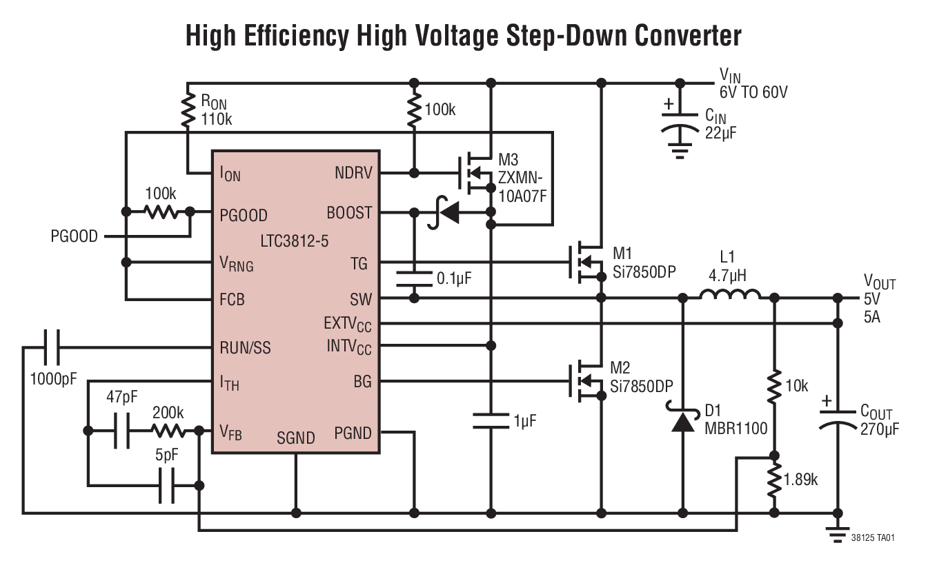
DC1035A
Analog Devices Inc.The LTC3812-5 is a synchronous step-down switching regulator controller that can directly step down voltages from up to 60V input, making it ideal for telecom and automotive applications. The LTC3812-5 uses a constant on-time valley current control architecture to deliver very low duty cycles with accurate cycle-by-cycle current limit without requiring a sense resistor.A precise internal reference provides 0.5% DC accuracy. A high bandwidth (25MHz) error amplifier provides very fast line and load transient response. Large 1? gate drivers allow the LTC3812-5 to drive large power MOSFETs for higher current applications. The operating frequency is selected by an external resistor and is compensated for variations in VIN. A shutdown pin allows the LTC3812-5 to be turned off reducing the supply current to

LT3470EDDB Demo Board | (DFN) 5.5V ≤ VIN ≤ 40V, VOUT = 5V @ 200mA, Integrated Boost and Catch Diodes
Analog Devices Inc.Demonstration circuit 1037 is a 40V micropower DFN buck regulator featuring the LT3470. The board is optimized for 5V output at up to 200mA load current for a steady state input voltage range of 5.5V to 40V. With its wide input voltage range, high efficiency internal power switch, low dropout operation, hysteretic current-mode, integrated boost and catch diodes and tiny SOT-23 package, the LT3470 is a very versatile and powerful IC for DC/DC converters that require extremely compact space, high efficiency and high input voltage.


