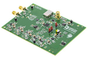
LTC6952 Demo Board | Ultralow Jitter, 4.5GHz PLL with 11 Outputs and JESD204B Support
Analog Devices Inc.The LTC6952 is a high performance, ultralow jitter,JESD204B/C clock generation and distribution IC. Itincludes a Phase Locked Loop (PLL) core, consisting ofa reference divider, phase-frequency detector (PFD) witha phase-lock indicator, ultralow noise charge pump andinteger feedback divider. The LTC6952?s eleven outputscan be configured as up to five JESD204B/C subclass1 device clock/SYSREF pairs plus one general purposeoutput, or simply eleven general purpose clock outputs fornon-JESD204B/C applications. Each output has its ownindividually programmable frequency divider and outputdriver. All outputs can also be synchronized and set toprecise phase alignment using individual coarse half-cycledigital delays and fine analog time delays.For applications requiring more than eleven total outputs,multiple LTC6952s can be connected together using theEZSync or ParallelSync synchronization protocols.Applications High Performance Data Converter Clocking Wireless Infrastructure Test and Measurement
LTC6955/LTC6955-1: Ultralow Jitter 11 Output Fanout Buffer
Analog Devices Inc.Demonstration Circuit 2611A features the LTC6955-1, Ultralow Jitter 11 Output Fanout Buffers.
By default, the DC2611A is powered from a single 3.3V supply. An option is provided to power to the DC2611A from dual supplies, allowing for the LTC6955-1’s output supply pins to connect to an LTC Silent Switcher® and the LTC6955-1 input supply pin to connect to a low noise LDO.
The differential inputs and six of the differential outputs are populated with 0.5" spaced SMA connectors. These outputs are AC-coupled with 50Ω transmission lines making them suitable to drive 50Ω impedance instruments. All registered trademarks and trademarks are the property of their respective owners.
The remaining four differential outputs are terminated with 100Ω.
A calibration path is provided to aid in accurate LTC6955-1 propagation delay measurements. The calibration path can be also reconfigured as a DC path, which allows for a convenient method of locking the LTC6955-1 outputs to an external PLL/VCO.
LTC2972 2-Channel PMBus Power System Manager with Eight Power Supply Rails
Analog Devices Inc.The DC2619A is a demonstration system for the LTC2972 power system manager that interfaces to various regulators. The board contains all the circuitry needed to demonstrate a power system that utilizes four 2-channel LTC2972 devices that manage eight power supplies. The eight power supplies include linear and switching regulators or the purpose of demonstrating a variety of methods to sense voltage and current. The demo board provides a sophisticated 8-channel programmable power supply system.
The LTC2972 is a 2-channel I2C/SMBus/PMBus power system manager that features accurate input current and energy measurement. The device monitors input current and input voltage, and calculates input power and energy. The DC2619A demonstrates the ability of the LTC2972 to sequence, trim, margin, supervise, monitor, and log faults for eight power supplies. The LTC2972 monitors each channel’s output voltage and output current and also monitors external temperature sensors and its own internal die temperature.
The DC2619A board contains eight independent power supply rails. The +5V/–5V rails are based on the switched capacitor LTC3260 regulator, the 1.0V/1.2V rails are powered by an LTC3633 switching regulator, the 1.5V/1.8V rails are powered by LTC3405A switching regulators, and the 2.5/3.3V rails are powered by LT3086/LT3055 linear regulators. The board is pre-configured with these voltages and may be re-configured with feedback resistors.
The LTpowerPlay® graphical user interface (GUI) supports this demonstration system and enables complete control of all the features of the LTC2972. Together, the LTpowerPlay software and DC2619A hardware system create a powerful development environment for designing and testing configuration settings of the LTC2972. LTpowerPlay stores these settings in the LTC2972’s internal EEPROM or in a project file. The software displays all of the configuration settings and real time measurements from the power system management IC. Telemetry allows easy access and decoding of the fault log created by the LTC2972. The board comes preprogrammed with the EEPROM values appropriate for the eight power supply rails on the DC2619A. Just plug and play!
Order pre-programmed devices from Linear Express® using LTpowerPlay.
The following items are required:
+12VDC Power Supply
USB-to-I2C/SMBus/PMBus Controller (DC1613)
LTpowerPlay Software
LTM4678 Demo Board | Dual 25A or Single 50A μModule Regulator with Digital Power System Management 4x LTM4678; 200A
Analog Devices Inc.Demonstration circuit 2638A-C is a high efficiency, high density, μModule regulator with 4.5V to 16V input range. The output voltage is adjustable from 0.5V to 3.3V, and it can supply 200A maximum load current. The demo board has four LTM4678 μModule® regulators, and the LTM4678 is a dual 25A or single 50A step-down regulator with PMBus power system management. Please see LTM4678 data sheet for more detailed information.
DC2638A-C powers up to default settings and produce power based on configuration resistors without the need for any serial bus communication. This allows easy evaluation of the DC/DC converter. To fully explore the extensive power system management features of the part, download the GUI software LTpowerPlay® onto your PC and use ADI’s I2C/SMBus/PMBus dongle DC1613A to connect to the board. LTpowerPlay allows the user to reconfigure the part on-the-fly and store the configuration in EEPROM, view telemetry of voltage, current, temperature and fault status.
GUI Download: The software can be downloaded from: LTpowerPlay.
For more details and instructions of LTpowerPlay, please refer to LTpowerPlay GUI for LTM4678 Quick Start Guide.
DC2642A-A
Analog Devices Inc.The LTC4041 is a complete supercapacitor backup system for 2.9V to 5.5V supply rails. It contains a high current step-down DC/DC converter to charge a single supercapacitor or two supercapacitors in series. When input power is unavailable, the step-down regulator operates in reverse as a step-up regulator to backup the systemoutput from the supercapacitor(s).The LTC4041?s adjustable input current limit function reduces charge current to protect the input supply from overload while an external disconnect switch isolates theinput supply during backup. When the input supply drops below the adjustable PFI threshold, the 2.5A boost regulator delivers power from the supercapacitor to the systemoutput.An optional input overvoltage protection (OVP) circuit protects the LTC4041 from high voltage damage at the VIN pin. An internal supercapacitor balancing circuit maintainsequal voltages across each supercapacitor and limits the maximum voltage of each supercapacitor to a pre-determined value. The LTC4041 is available in a low profile (0.75mm) 24-Lead 4mm ? 5mm QFN package.ApplicationsRide-Through ?Dying Gasp? SuppliesHigh Current Ride-Through 3V to 5V UPSPower Meters/Industrial AlarmsServers/Solid State Drives
DC2654A
Analog Devices Inc.The LTC4162-L is an advanced monolithic synchronous step-down switching battery charger and PowerPath? manager that seamlessly manages power distribution between input sources such as wall adapters, backplanes, solar panels, etc., and a rechargeable Lithium-Ion/Polymer battery.A high resolution measurement system provides extensive telemetry information for circuit voltages, currents, battery resistance and temperature which can all be read back over the I2C port. The I2C port can also be used to configure many charging parameters including charging voltages and currents, termination algorithms and numerous system status alerts.The LTC4162-L can charge Lithium-Ion cell stacks from 1 cell to 8 cells with as much as 3.2A of charge current.The power path topology decouples the output voltage from the battery allowing a portable product to start up instantly under very low battery voltage conditions.The LTC4162-L is available in a thermally enhanced 28-pin 4mm ? 5mm ? 0.75mm QFN surface mount package.
VCO Rider Board with Loop Filter
Analog Devices Inc.Demonstration circuit 2664A is a VCO Rider Board with Loop Filter that supports the popular 0.5" × 0.5" VCO package footprint.
The DC2664A expedites evaluation of Phase-Locked Loop (PLL) devices requiring an external Voltage Controlled Oscillator (VCO). Without the DC2664A, each
VCO and PLL combination requires a unique loop filter design, resulting in several PLL demo board modifications to evaluate each VCO. These board modifications
are time consuming and often result in damage to either the PLL or the VCO.
The DC2664A integrates the VCO and loop filter allowing these unique designs to reside on multiple DC2664As. The DC2664A RFOUT and VTUNE SMA connections allow the user to quickly evaluate a PLL with multiple VCOs without risk of damage from multiple board modifications.
VCOs are notoriously sensitive to power supply noise and spurs. The DC2664A resolves the concern of locating a low noise and low spurious lab supply by powering the VCO with an onboard ultralow noise and ultrahigh PSRR LDO, the LT3042. A second LT3042 LDO is available on the DC2664A to power an active loop filter. Both LDOs
are powered from a single supply, simplifying the number of lab supplies required to evaluate a VCO and PLL combination.
The DC2664A was designed to mate directly with the LTC6955 (DC2611A) and LTC6952 (DC2609A) demo boards.
LTC7862EUFD Demo Board | 8V ≤ VIN(Normal) ≤ 32V, Surge to 140V; 32.7V ≤ VOUT(Clamp) ≤ 35V @ 10A
Analog Devices Inc.Demonstration circuit 2674A is a 140V high efficiency
switching surge stopper featuring the LTC7862. The
board operates from an input voltage range of 8V to
140V, and provides a 8V to 34V output from 0A to 10A.
Its output voltage is programmed to be clamped at 34V
(typical) with a minimum ride-through duration of 500ms
to allow the load to operate through the input overvoltage
events. Its output current is limited to protect against
output short-circuit faults. A soft-start feature is utilized
to control its output voltage slew rate at start-up and input
voltage transients. This feature reduces current surge and
output voltage overshoot. The demonstration board is
able to achieve low insertion drop (210mV typical) by
utilizing the low RDS(ON) N-channel MOSFETs and low
DCR inductor. This board also includes optional reverse
polarity protection circuit which protects the downstream
loads up to −40V. The demonstration circuit is suitable
for a wide range of automotive, industrial, and telecom
applications.
The LTC7862 high efficiency switching surge stopper
protects loads from input high voltage transients. During
an input overvoltage event, the LTC7862 controls the
gate of two external N-channel MOSFETs and operate as
a switching DC/DC step-down regulator. The output voltage
is maintained at a safe level, allowing the loads to
continue to operate through the input overvoltage events.
During normal operation, the LTC7862 turns on the top
external N-channel MOSFET continuously, passing the
input voltage through to the output with minimal voltage
drop. The LTC7862 also limits the maximum output current
to protect against overcurrent and short-circuit faults.
A programmable timer limits the time that the LTC7862
can spend switching during an overvoltage, overcurrent,
or startup condition. When the timer expires, the external
MOSFETs are turned off for a cooldown period and
then the LTC7862 restarts. The timer limits how long the
LTC7862 can switch when the power loss is relatively
high, the components and thermal design can be optimized
for normal pass-through operation.
The LTC7862 data sheet gives a complete description
of the part, operation and application information. The
data sheet must be read in conjunction with this demo
manual for DC2674A. Proper board layout is essential
for maximum thermal and electrical performance. See the
data sheet sections for details. The LTC7862 is available
in 20-lead TSSOP and QFN packages and two operating
junction temperature grades: industrial (−40°C to 125°C)
and high temperature automotive (−40°C to 150°C).
LT3960 and LT3967 Demo Board | 1.3A 8-Switch Matrix LED Dimmer with I2C to CAN-Physical Layer Transceiver
Analog Devices Inc.Demonstration circuit 2686A is a 1.3A 8-switch matrix LED dimmer system with an I2C to CAN-physical transceiver featuring the LT3967 and LT3960. This demonstration circuit connects directly to a LED string and LED driver demonstration circuit to allow for independent dimming control of up to 8 channels of LEDs. A Linduino® One demonstration circuit is used to interface with the board and can connect in one of two different ways:
Connect directly to a Linduino One demonstration circuit with a QuikEval™ ribbon cable.
Connect using the LT3960 break-off board to connect to the I2C master device, but pass data over two twisted pair lines to the LT3960 on the main PCB.
The LT3967 matrix dimmer features 8 individually con-trolled 1.3A rated floating NMOS switch channels and can support up to 56V of LEDs per device. The channels of the LT3967 can be configured for series connections, or non-series connections. Additional DC2686A demo circuits can be connected in series for higher number of LEDs, or in parallel to allow for higher current operation. Resistors are used to configure both the I2C slave address as well as the default start-up state. The default configuration for DC2686A sets the I2C address as 0000 with all LEDs off. See the LT3967 data sheet for details.
The LT3960 I2C to CAN-Physical transceiver is used to send and receive I2C data through harsh or noisy environments at up to 400kb/s using the CAN-Physical layer for differential signaling over twisted pair connections. Both SDA and SCL data lines are converted to differential signals and are shared between devices connected to the bus. This allows for physical separation of the I2C source with the LT3960 transceiver board and the LT3967 main PCB along with the LED driver.
This demo circuit is designed to be easily configured and interfaced with a compatible low output capacitance LED driver and LED string. It can easily be directly attached to a buck LED driver or a floating buck-mode LED driver. More sophisticated setups with series matrix dimmers for higher number of LEDs such as 12 or 16 is possible. Please consult factory applications for details or look for more details on analog.com.
The LT3967 and LT3960 data sheets give complete description of the parts, their operation and applications information. The data sheets must be read in conjunction with the demo manual for demonstration circuit DC2686A. The LT3967EFE is assembled in a thermally enhanced 28-lead TSSOP package. The LT3960EMSE is assembled in a 10-lead MSOP package.
DC2705A
Analog Devices Inc.The LTC4376 is a 7A ideal diode that uses an internal 15m? N-channel MOSFET to replace a Schottky diode when used in diode-OR and high current diode applications. The LTC4376 reduces power consumption, heat dissipation and PC board area.The LTC4376 controls the forward voltage drop across the internal MOSFET to ensure smooth current delivery without oscillation even at light loads. If a power source fails or is shorted, a fast turn-off minimizes reverse current transients. The LTC4376 also easily ORs power sources to increase total system reliability.With its low operating voltage, small solution size and the ability to withstand reverse input voltage, the LTC4376 excels in portable battery applications. A shutdown mode is available to reduce the quiescent current to 9?A. The SHDN pin can also control the forward current path when an external MOSFET is used in series with the internal MOSFET in a back-to-back configuration.Applications Automotive Battery Protection Redundant Power Supplies Portable Battery Devices Computer Systems/Servers
DC2708A
Analog Devices Inc.The LTC7001 is a fast high side N-channel MOSFET gate driver that operates from input voltages up to 135V. It contains an internal charge pump that fully enhances an external N-channel MOSFET switch, allowing it to remain on indefinitely.Its powerful driver can easily drive large gate capacitances with very short transition times, making it well suited for both high frequency switching applications or static switch applications that require a fast turn-on and/or turn-off time.The LTC7001 is available in the thermally enhanced 10-lead MSOP package.APPLICATIONS Static Switch Driver Load and Supply Switch Driver Electronic Valve Driver High Frequency High Side Gate Driver
LTC1628CG | Dual Phase Multi-Output High Current Converter, 7V to 24V Input, VOUT1 = 5V @ 12A Max., VOUT2 = 3.3V @ 12A Max.
Analog Devices Inc.DC271A: Demo Board for the LTC1628 High Efficiency, 2-Phase Synchronous Step-Down Switching Regulator.
DC2737A
Analog Devices Inc.The LT8301 is a micropower isolated flyback converter. By sampling the isolated output voltage directly from the primary-side flyback waveform, the part requires no third winding or opto-isolator for regulation. The output voltage is programmed with a single external resistor. Internal compensation and soft-start further reduce external component count. Boundary mode operation provides a small magnetic solution with excellent load regulation. Low ripple Burst Mode operation maintains high efficiency at light load while minimizing the output voltage ripple. A 1.2A, 65V DMOS power switch is integrated along with all high voltage circuitry and control logic into a 5-lead ThinSOT? package.The LT8301 operates from an input voltage range of 2.7V to 42V and can deliver up to 6W of isolated output power. The high level of integration and the use of boundary and low ripple burst modes result in a simple to use, low component count, and high efficiency application solution for isolated power delivery.Applications Isolated Telecom, Automotive, Industrial, Medical Power Supplies Isolated Auxiliary/Housekeeping Power Supplies
DC2739A
Analog Devices Inc.The LTC2972 is a 2-channel Power System Manager used to sequence, trim (servo), margin, supervise, manage faults, provide telemetry and create fault logs. PMBus commands support power supply sequencing, precision point-of-load voltage adjustment and margining. DACs use a proprietary soft-connect algorithm to minimize supply disturbances. Supervisory functions include over and under voltage and temperature threshold limits for two power supply output channels as well as over and under voltage threshold limits for a single power supply input channel. Programmable fault responses can disable the power supplies with optional retry after a fault is detected. Faults that disable a power supply can automatically trigger black box EEPROM storage of fault status and associated telemetry. An internal 16-bit ADC monitors two output voltages, two output currents, two external temperatures, input voltage and current, and die temperature. Input power, energy, and output power are also calculated. A programmable watchdog timer monitors microprocessor activity for a stalled condition and resets the microprocessor if necessary. A single wire bus synchronizes power supplies across multiple ADI Power System Management (PSM) devices. Configuration EEPROM with ECC supports autonomous operation without additional software.APPLICATIONS Computers and Network Servers Industrial Test and Measurement High Reliability Systems Video and Medical Imaging
LTC3315A Demo Board | Dual 5V, 2A Synchronous Step-Down DC/DCs in 2mm × 2mm LQFN
Analog Devices Inc.Demonstration Circuit DC2747A features the LTC3315A dual 5V, 2A Synchronous Step-Down DC/DC regulators operating at 2.0MHz. One regulator provides a 1.2V output and the other provides 1.8V, both up to a 2A load. The LTC3315A supports adjustable output voltages from 0.5V to VIN, operating frequencies from 1MHz up to 3MHz. The LTC3315A is a compact, high efficiency, and high speed synchronous monolithic step-down switching regulator. Fast minimum on-time of 25ns enables high VIN to low VOUT conversion at high frequency.
The DC2747A operating mode may be selected as Burst Mode operation, Skip mode or Forced Continuous (FC) mode. Setting JP1 to the FC/SYNC position will allow the LTC3315A to sync to a clock frequency from 1MHz to 3MHz. The LTC3315A operates in Forced Continuous mode when syncing to an external clock.
The LTC3315A data sheet gives a complete description of the device, operation and application information. The data sheet must be read in conjunction with this demo. The LTC3315A is assembled in a 2mm × 2mm LQFN package with exposed pads for low thermal resistance. The PCB Considerations section in the data sheet.
The Efficiency vs Load graph shows the efficiency and the power loss of the circuit with a 3.3V input in Burst Mode operation.
DC2749A
Analog Devices Inc.The LTC7003 is a fast high side N-channel MOSFET gate driver that operates from input voltages up to 60V. It contains an internal charge pump that fully enhances an external N-channel MOSFET switch, allowing it to remain on indefinitely.Its powerful driver can easily drive large gate capacitances with very short transition times, making it well suited for both high frequency switching applications or static switch applications that require a fast turn-on and/or turn-off time.When an internal comparator senses that the switch current has exceeded a preset level, a fault flag is asserted and the switch is turned off after a period of time set by an external timing capacitor. After a cooldown period, the LTC7003 automatically retries.The LTC7003 is available in the thermally-enhanced 16-lead MSOP package.APPLICATIONS Static Switch Driver Load and Supply Switch Driver Electronic Valve Driver High Frequency High Side Gate Driver
LTC4331 Demo Board
Analog Devices Inc.Demonstration circuit 2754A extends an I2C based QuikEval™ interface to up to 450 feet and features the LTC4331. In order to realize the QuikEval interface, this demo circuit includes two complete I2C extenders and a remote side power supply formed from an LT3461 boost converter and two LT1761 LDOs.
The LTC4331 is a SMBus compatible I2C slave device extender designed for operation in high noise industrial environments. The I2C/SMBus is extended over a single twisted pair by a ±60V fault protected differential transceiver. The LTC4331’s extended 15V common mode voltage range allows it to bridge across different ground potentials.
When used as a QuikEval extender, the DC2754A requires the use of the DC2026 USB serial adapter. The DC2754A is NOT compatible with the DC590 USB serial adapter because the DC590 does not support clock stretching.
The DC2754A’s jumpers and turrets allow easy re-configuration for use in other applications and/or demonstrating other application circuits. The circuit board is fabricated with a score between the local and remote sides to allow physical separation. The link cable connections are made using either pluggable terminal blocks or an Ethernet cable.
Two complete I2C extenders are present. The first extender has a full set of diagnostic LEDs, jumpers, turrets and large (0805) resistors for simple user reconfiguration and connection for customer specific application(s). The second extender is configured specifically for the QuikEval EEPROM with no LEDs; however, it may be reconfigured and used for customer specific application(s) via 0603 jumpers and resistors and unpopulated test points on 0.1" centers.
The LTC4331 data sheet gives a complete description of the part, its operation and application information. The data sheet should be referred to when reading this demo manual. The LTC4331 is available in a 20-lead QFN package and three temperature grades (commercial 0°C to 70°C, industrial –40°C to 85°C, and high temperature –40°C to 125°C).
Demo Board for LTC6754 High Speed Comparator with LVDS
Analog Devices Inc.Demonstration circuit 2767A features the LTC6754 highspeed rail-to-rail comparator in a QFN package with LVDS
compatible outputs. The DC2767 input is AC-coupled for
single-ended signal greater than 5MHz and up to 445MHz.
The DC2767 outputs are AC-coupled 50Ω source impedance for driving directly the 50Ω inputs of a 1GHz or
higher oscilloscope. The DC2767 has a supply connection
for the LTC6754 rail-to-rail inputs and a separate supply
connection for the QFN LTC6754 LVDS outputs.
The LTC6754 includes 4.5mV of hysteresis to minimize
instability. For the QFN package, a separate pin is available to set the hysteresis from 0mV (off) up to 40mV. The
QFN version also features output latching to provide the
ability to capture the state of the comparator. The DC2767
provides a connection to set the hysteresis or for output
latching.
LTC6754 is ideally suited for high frequency line driver
and clock recovery circuits.
DC2769A-A-KIT
Analog Devices Inc.The LTC4124 is a simple high performance wireless Li-Ion charger with low battery disconnect. The pin-selectable charge current (up to 100mA) and charge voltage ensure versatility while minimizing the number of required external components.Wireless charging with the LTC4124 allows devices to be charged while sealed within enclosures and eliminates bulky connectors in space-constrained applications. Elimination of exposed conductive connectors also creates more robust devices while ensuring an effortless end-user experience.The LTC4124 includes an NTC input for safe temperature qualified charging and a battery disconnect feature that prevents damage to a battery due to over-discharging.The 2mm ? 2mm LQFN package and minimal number of external components make the LTC4124 well-suited for low power portable applications where small solution size is mandatory.Applications Medical Wireless Sensors Military Wearables High End Wireless Headsets Streaming Headsets with Bluetooth Connectivity Virtual Reality Headsets High End Remote Control IoT Devices
LTC7821 Demo Board | 40V ≥ VIN ≥ 60V, VOUT = 12V @ 100A
Analog Devices Inc.Demonstration circuit 2787A is a high efficiency, 4 phase, hybrid converter. It can deliver 12V/100A with the input voltage from 40V to 60V. The demo board features the LTC7821, which uses an architecture that merges a soft-switching switched-capacitor topology with a traditional step-down converter to provide superior efficiency compared to the traditional switching architectures. It offers a high efficiency/high density and cost effective solution for nonisolated intermediate bus applications in power distribution, datacom and telecom as well as emerging 48V automotive systems.
External MOSFETs switch at a 400kHz fixed frequency for this demo board and can be programmed from 200kHz to 1.5MHz. The LTC7821’s powerful 1Ω N-channel MOSFET gate drivers maximize efficiency and can drive multiple MOSFETs in parallel for higher power applications. Due to its current mode control architecture, multiple LTC7821 devices can be operated in a parallel, multiphase configuration with excellent current sharing and low output voltage ripple to enable much higher power applications. Other benefits include low EMI emissions due to a soft-switched front end and reduced MOSFET stress.
The LTC7821 design eliminates the inrush current typically associated with switched capacitor circuits by prebalancing the capacitors on start-up. The LTC7821 also monitors system voltage, current and temperature for faults, and uses a sense resistor for overcurrent protection. It stops switching and pulls the FAULT pin low when a fault condition occurs. An onboard timer can be set for appropriate restart/retry times. Additional features include ±1% output voltage accuracy over temperature, a clock output for multiphase operation, a power good output signal, short-circuit protection, monotonic output voltage start-up, optional external reference, undervoltage lockout and internal charge balance circuitry. The LTC7821 data sheet must be used in conjunction with this demo board manual.


