EV1HMC891ALP5
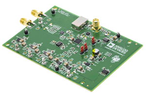
Analog Devices Inc.The HMC891ALP5E is a monolithic microwave integrated circuit (MMIC) band-pass filter that features a user-selectablepass band frequency. The 3 dB filter bandwidth is approximately 9% and the 20 dB filter bandwidth is approximately 23%. Thecenter frequency (fCENTER) can be varied between 1.95 GHz and 3.4 GHz by applying an analog tune voltage between 0 V and 14 V.This tunable filter can be used as a smaller alternative to physically large switched filter banks and cavity tuned filters.The HMC891ALP5E has excellent microphonics due to the monolithic design, and provides a dynamically adjustablesolution in advanced communications applications.ApplicationsTesting and measurement equipmentMilitary radar and electronic warfare/electronic counter measure (ECM)Satellite communication and spaceIndustrial and medical equipment
ADI LISTN™ EZ-Audio System
Analog Devices Inc.The ADI LISTN EZ-Audio System (EV-21562-AUTO) enables rapid tuning and deployment of a pre-configured 4-channel in/12-channel out audio flow from DSP Concepts running on the ADSP-2156x family (ADSP-21562/ADSP-21563/ADSP-21565) of SHARC audio processors. Using a custom tuning tool (AWE Tune), customers can quickly tailor the audio output for any automotive cabin. Reduce your time to audio using this turnkey hardware/software automotive audio solution jointly developed by Analog Devices and DSP Concepts.
ADI LISTN EZ-AUDIO System Customer Journey
EV2HMC618ALP3
Analog Devices Inc.The HMC618ALP3E is a GaAs pHEMT MMIC Low Noise Amplifier that is ideal for Cellular/3G and LTE/WiMAX/4G basestation front-end receivers operating between 1.2 - 2.2 GHz. The amplifier has been optimized to provide 0.75 dB noise figure, 19 dB gain and +36 dBm output IP3 from a single supply of +5V. Input and output return losses are excellent and the LNA requires minimal external matching and bias decoupling components. The HMC618ALP3E shares the same package and pinout with the HMC617LP3E 0.55 - 1.2 GHz LNA. The HMC618ALP3E can be biased with +3V to +5V and features an externally adjustable supply current which allows the designer to tailor the linearity performance of the LNA for each application. The HMC618ALP3E offers improved noise figure versus the previously released HMC375LP3(E) and the HMC382LP3(E).Applications Cellular/3G and LTE/WiMAX/4G BTS & Infrastructure Repeaters and Femto Cells Public Safety Radio
EV2HMC788ALP2
Analog Devices Inc.The HMC788A is a 0.01 GHz to 10 GHz, gain block, monolithic microwave integrated circuit (MMIC) amplifier using gallium arsenide (GaAs), pseudomorphic high electron mobility transistor (pHEMT) technology.This 2 mm ? 2 mm LFCSP amplifier can be used as either a cascadable 50 ? gain stage, or to drive the local oscillator (LO) port of many of the single and double balanced mixers from Analog Devices, Inc. with up to 20 dBm output power.The HMC788A offers 14 dB of gain and an output IP3 of 33 dBm while requiring only 76 mA from a 5 V supply.The Darlington feedback pair exhibits reduced sensitivity to normal process variations and yields excellent gain stability over temperature while requiring a minimal number of external bias components.Applications Cellular, 3G, LTE, WiMAX, and 4G LO driver applications Microwave radio Test and measurement equipment Ultra wideband (UWB) communications
EV-AD1018EBZ
Analog Devices Inc.The AD1018 is an analog front end (AFE) that has a high precision analog-to-digital converter (ADC), voltage output digital-to-analog converters (VDACs), and current output digital-to-analog converters (IDACs). The ADC signal chain contains four transimpedance amplifier inputs (TIAs), 17 external voltage inputs, nine VDAC monitor channels, 11 IDAC monitor channels, a precharge buffer, and a 1 MSPS successive approximation register (SAR) ADC. The TIAs convert an input current to voltage and use an internal 2.5 V ADC reference for the positive terminal. The input multiplexer selects and configures either one of the channels (TIAx_OUT, AINx, IDACx, or VDACx) or one of the internal power monitor signals (AVDDx ? 3/8, IOVDD ? 3/8, PVDD_IDACx, or AGNDx) as an output to the SAR ADC input. These inputs are single-ended. AGNDx is used as the reference signal. An ADC sequencer option is also available to program an automatic channel measurement sequence (see the AD1018 Hardware Reference Manual for more information). The AD1018 provides 11 channels of low noise, low drift IDAC outputs with a full-scale range (0 mA to 20 mA or 0 mA to 50 mA for IDAC0 to IDAC6, and 0 mA to 150 mA or 0 mA to 200 mA for IDAC7 to IDAC10). Each IDAC channel has 16-bit resolution. The AD1018 has nine VDAC channels with 16-bit resolution. Each channel has a voltage output buffer. A 2.5 V on-chip reference buffer can drive a 100 nF capacitive load and maximum load current of 10 mA. This buffer is designed to bias an external thermal resistor. Use the 4-wire serial port interface (SPI) at up to 40 MHz to configure each block and to gather ADC data.APPLICATIONS Optical communication modules
EV-AD12CSBZ
Analog Devices Inc.The ADRF8800/ADRF8850 are low power, integrated systems on chip (SoC) that include a 2.4 GHz (industrial scientific medical) ISM band radio and an embedded microcontroller unit (MCU) subsystem.The ADRF8800/ADRF8850 provide wireless communications between the battery cell monitoring chip and the battery management system (BMS) controller. In the wireless battery management system (wBMS), the ADRF8800 nodes reside at the battery cells and take sensor data from the battery cell monitors. The nodes send the data over the air to an ADRF8850 network manager, and the manager provides the data to the BMS controller. The ADRF8850 network manager configures the network of nodes and manages the communications protocol.The embedded MCUs integrate static random access memory (SRAM), embedded flash memory, one-time programmable (OTP) memory, and an analog subsystem that provides clocking and reset.The ADRF8800/ADRF8850 has a rich set of peripherals, including serial peripheral interface (SPI), general-purpose input and output (GPIOs) ports, universal asynchronous receiver/transmitter (UART), and Joint Test Action Group (JTAG) port, as well as an analog-to-digital converter (ADC) and temperature sensor.The ADRF8800/ADRF8850 provide secure boot using software stored in read only memory (ROM) that authenticates the next boot stage using a hardware accelerated 256-bit elliptic curve cryptography (ECC-256) engine. Other hardware accelerated cryptographic features include the 128-bit advanced encryption standard (AES-128), 256-bit advanced encryption standard (AES-256), and Secure Hash Algorithm 256 (SHA-256). The ADRF8800/ADRF8850 have protected key storage with a root encrypted key generated on-chip that is only accessible to the on-chip hardware. The devices incorporate a true random number generator (TRNG) that is used to seed a National Institute of Standards and Technology (NIST) certified deterministic random bit generator (DRBG). The ADRF8800/ADRF8850 also include support for secure firmware updates with rollback protection. The in-field OTP memory is included to enforce the access control of debug ports and memory access once a device is ready for deployment.The ADRF8800/ADRF8850 feature on-chip, low dropout (LDO) regulators that allow the devices to be powered by a single 3.3 V nominal supply, provided by an external power management IC (PMIC) either stepping down from a high voltage bus or a 12 V battery.Each ADRF8800/ADRF8850 uses a single 40 MHz crystal to provide precision timing for the system.The ADRF8800/ADRF8850 are available in a 7 mm ? 7 mm body size, 48-lead LQFP_EP package, measuring 9 mm ? 9 mm when leads are included.APPLICATIONS Wireless Battery Management Systems
EV-AD7284SSSDZ
Analog Devices Inc.The AD7284 contains all the functions required for the general-purpose monitoring of stacked Li-Ion batteries, as used in hybrid electric vehicles and battery backup applications.The AD7284 has multiplexed cell voltage and auxiliary, analog-to-digital converter (ADC) measurement channels supporting four to eight cells of battery management. The device provides a maximum total unadjusted error, TUE, (cell voltage accuracy) of ?3 mV that includes all the internal errors from input to output. The primary ADC resolution is 14 bits.The AD7284 also includes an integrated secondary measurement path that validates the data on the primary ADC. Other diagnostic features include the detection of open inputs, communication, and power supply related faults.The AD7284 cell balancing interface outputs control the external field effect transistors (FETs) to allow discharging of individual cells.There are two on-chip 2.5 V voltage references: one reference for the primary measurement path, and one for the secondary measurement path.The AD7284 operates from one VDD supply, ranging from 10 V to 40 V. The device provides eight differential analog input channels to accommodate large common-mode signals across the full VDD range. Each channel allows an input signal range, VPINx ? VPIN(x ? 1) and VSINx ? VSIN(x ? 1), of 0 V to 5 V, where x = 0 to 8. The input pins assume a series stack of eight cells. The AD7284 includes four auxiliary ADC input channels that can be used for temperature measurement or system diagnostics.The AD7284 has a differential daisy-chain interface that allows multiple devices to be stacked without the need for individual device isolation. By design, this interface allows both device to device communication within the same module and communication between devices on different modules.Applications Li-Ion battery monitoring Electric and hybrid electric vehicles Stationary power applications
EV-AD74413RSDZ
Analog Devices Inc.The AD74413R is a quad-channel software configurable input/output solution for building and process control applications. The AD74413R contains functionality for analog output, analog input, digital input, resistance temperature detector (RTD), and thermocouple measurements integrated into a single chip solution with a serial peripheral interface (SPI).The device features a 16-bit, ?-? analog-to-digital converter (ADC) and four configurable, 13-bit digital-to-analog converters (DACs) to provide four configurable input/output channels and a suite of diagnostic functions.?There are several modes related to the AD74413R. These modes are voltage output, current output, voltage input, externally powered current input, loop powered current input, external RTD measurement, digital input logic, and loop powered digital input.?The AD74413R contains a high accuracy 2.5 V internal reference to drive the DACs and the ADC.?Product Highlights Quad-Channel, Software Configurable Channels. Built In Diagnostics and Alert Features. Robust Architecture.?Applications? Process control Factory automation Motor drives Building control systems?
DC2965A
Analog Devices Inc.The LTC3336 is a compact high efficiency nanopower hysteretic buck DC/DC which can deliver up to 250mA of output current from a 2.5V to 15V input. Input quiescent current is typically 80nA with the output in regulation at no load for output voltages less than 2.4V; this number is reduced further for higher output voltages at which internal circuits can be boot-strapped from the output. Performance specifications are ideal for primary (i.e., non-rechargeable) battery powered applications: low IQ plus the ability to set the peak current to a level matched to the battery?s maximum capacity point.The peak input currents of 10mA, 30mA, 100mA, and 300mA are pin selectable as well as the output voltages of 1.2V, 1.5V, 1.6V, 1.8V, 2.0V, 2.4V, 2.5V, 2.8V, 3.0V, 3.2V, 3.3V, 3.6V, 3.7V, 4.1V, 4.2V, and 5.0V.The LTC3336 is offered in a compact 12-lead 2mm ? 2mm LQFN package.APPLICATIONS Low Power Primary Battery Powered Systems (e.g., 1? ? 3? Li-Ion Primary, 3? ? 8? AAA) Remote Industrial Sensors (e.g., Meters, Alarms) Asset Trackers Electronic Door Locks Keep-Alive Supplies/Battery Backup SmartMesh? Applications
LT1361CS8, LT1210CR | Mobile-CPU VRM Tester, 1 Input, 3 Output with 15A Load Pulser
Analog Devices Inc.DC296A Demo Board for:
LT1361 Dual and Quad 50MHz, 800V/µs Op Amps
LT1210 1.1A, 35MHz Current Feedback Amplifier (CFA)
LT1270CT | Ring Tone Power Supply with Shutdown, +5 VIN to Isolated +100V/-100 VOUT
Analog Devices Inc.DC297A: Demo Board for LT1270 8A and 10A High Efficiency Switching Regulators.
DC2987A
Analog Devices Inc.The LT3935 is a monolithic, synchronous, step-down DC/DC converter that utilizes fixed-frequency, peak current control and provides PWM dimming for a string of LEDs. The LED current is programmed by an analog voltage or the duty cycle of pulses at the CTRL pin. An output voltage limit can be set with a resistor divider to the FB pin.The switching frequency is programmable from 200kHz to 2MHz by an external resistor at the RT pin or by an external clock at the SYNC/SPRD pin. With the optional spread spectrum frequency modulation enabled, the frequency varies from 100% to 125% to reduce EMI.Additional features include an LED current monitor, an accurate EN/UVLO pin threshold, open-drain fault reporting for open-circuit and short-circuit load conditions, and thermal shutdown. The LT3935 utilizes proprietary Silent?Switcher technology for very low EMI.APPLICATIONSAutomotive LightingIndustrial and General Purpose Lighting
LTM4657 Demo Board | 20VIN, 8A Step-Down µModule® Regulator
Analog Devices Inc.Demonstration circuit 2989A features the LTM4657 µModule® regulator, a high performance, high efficiency step-down regulator. The LTM4657 is a complete DC/DC point-of-load regulator in a thermally enhanced 6.25mm x 6.25mm x 3.87mm BGA package. The LTM4657 has an operating input voltage range of 3.1V to 20V and provides an output current up to 8A. The output voltage is programmable from 0.6V to 5.5V and can be remotely sensed. The stacked inductor design improves thermal dissipation and significantly reduces the package area.
Output voltage tracking is available through the TRACK/SS pin for supply rail sequencing. External clock synchronization is available through the SYNC/MODE pin. For high efficiency at low load currents, select DCM mode operation using the MODE jumper (JP7) in less noise sensitive applications. The LTM4657 data sheet must be read in conjunction with this demo manual for working on or modifying DC2989A.
LTC3308A Demo Board | 5V Input to 1.2V Output at 4A Synchronous Step‑Down Silent Switcher Demo Circuit
Analog Devices Inc.Demonstration circuit 2991A features the LTC3308A 5V, 4A synchronous step-down Silent Switcher® operating as a 2.0MHz, 3.3V to 1.2V 4A buck regulator. The LTC3308A supports adjustable output voltages from 0.5V to VIN with operating frequencies from 1MHz up to 3MHz. The LTC3308A is a compact, ultralow emission, high efficiency, and high speed synchronous monolithic stepdown switching regulator. A minimum on-time switching of 22ns enables high VIN to low VOUT conversion ratios at high frequencies.
The DC2991A operating mode may be selected as BURST, SKIP or Forced Continuous (FC) mode. Setting JP1 to the FC/SYNC position will allow the LTC3308A to sync to a clock frequency from 1MHz to 3MHz. The LTC3308A operates in forced continuous mode when syncing to an external clock. The DC2991A is set to a fixed 2MHz frequency by connecting RT to VIN through a 0Ω resistor, R9. The frequency can be easily changed by removing R9 and setting an appropriate resistor in the R4 location to obtain the desired frequency. Refer to the LTC3308A data sheet for the proper RT value for a desired switching frequency.
The DC2991A also has an EMI filter to reduce conducted EMI. This EMI filter can be included by applying the input voltage at the VIN EMI terminal. The EMI performance of the board is shown in the EMI Test Results section. The red lines in the EMI performance graphs illustrate the CISPR25 Class 5 peak limits for the conducted and radiated emission tests.
The LTC3308A data sheet gives a complete description of the device, operation and application information. The data sheet must be read in conjunction with this demo manual. The LTC3308A is assembled in a 2mm × 2mm LQFN package with exposed pads for low thermal resistance. The layout recommendations for low EMI operation and maximum thermal performance are available in the data sheet section: Low EMI PCB Layout.
The Efficiency vs Load graph shows the efficiency and the power loss of the circuit with a 3.3V input in Burst Mode operation.
LTC7891 High Frequency Step-Down Supply with GaN FETs
Analog Devices Inc.Demonstration circuit 2995A is a buck regulator featuring the LTC7891. The DC2995A operates from a 36V to 72V input voltage range and generates a 12V, 20A output.
The LTC7891 has a precision voltage reference which can generate an output voltage with 2% tolerance over the full operating conditions. The 500kHz switching frequency operation results in a small and efficient circuit. The converter achieves over 96% efficiency with 20A load.
The demonstration circuit can be easily modified to regulate output voltages from 0.8V to 60V.
The DC2995A provides a high performance cost-effective solution for generating a 12V output. The LTC7891 data sheet gives a complete description of this part, its operation and application information and must be read in conjunction with the demo manual.
LT8640A | 42V, 5A (8A Peak) Synchronous Step-Down Silent Switcher with 2.5μA Quiescent Current
Analog Devices Inc.Demonstration circuit 3099A is a 42V, 5A synchronous step-down Silent Switcher® with spread spectrum frequency modulation featuring the LT8640A. The demo board is designed for 5V output from a 5.7V to 42V input. Meanwhile the LT8640A can operate down to 3.4V inputs. The wide input range allows a variety of input sources, such as automotive batteries and industrial supplies. The LT8640A is a compact, ultralow emission, high efficiency, and high speed synchronous monolithic stepdown switching regulator. The integrated power switches and inclusion of all necessary circuitry reduce the components count and solution size. Special Silent Switcher architecture minimizes EMI emissions. Selectable spread spectrum mode can further improve EMI performance. Ultralow 2.5μA quiescent current in Burst Mode® operation achieves high efficiency at very light loads. Fast minimum on-time of 30ns enables high VIN to low VOUT conversion at high frequency.
The LT8640A switching frequency can be programmed either via oscillator resistor or external clock over a 200kHz to 3MHz range. The default frequency of demo circuit 3099A is 2MHz. The LT8640A SYNC/MODE pin on the demo board is grounded (JP1 at BURST position) by default for low ripple Burst Mode operation. Spread spectrum mode and forced continuous mode can be selected respectively by moving JP1 shunt. To synchronize to an external clock, move JP1 to FCM/SYNC and apply the external clock to the SYNC terminal.
The LT8640A data sheet gives a complete description of the part, operation, and application information. The data sheet must be read in conjunction with this demo manual for demo circuit 3099A. The LT8640A is assembled in a 3mm × 4mm plastic QFN package with exposed pad for low thermal resistance. The layout recommendations for low EMI operation and maximum thermal performance are available in the data sheet section Low EMI PCB Layout and Thermal Considerations and Peak Output Current.
LT8722 | Monolithic Thermoelectric Cooler Driver
Analog Devices Inc.Demonstration circuit 3145A demonstrates a high efficiency thermoelectric cooler driver and features the LT8722 monolithic driver.
The input voltage range of the DC3145A is from 3.1V to 15V and the output is a SPI programmable differential voltage output. The maximum output current is 4A. The switching frequency SPI programmable from 500kHz to 3MHz.
The LT8722 is controlled through an SPI interface and therefore the demonstration circuit is also setup to interface through SPI. For demonstration purposes the manual provides instruction on how to connect the DC2026C Linduino board to monitor and control the DC3145A with a PC using a command line Arduino IDE interface.
LTC1546CG LTC1545CG | Software-Selectable Multiprotocol Transceiver with Termination and RL, RI, LL and TM
Analog Devices Inc.DC327A Demo Board for:
LTC1545 Software-Selectable Multiprotocol Transceiver
LTC1546 Software-Selectable Multiprotocol Transceiver with Termination
DC338B-A
Analog Devices Inc.The LTC1563-2/LTC1563-3 are a family of extremely easy-to-use, active RC lowpass filters with rail-to-rail inputs and outputs and low DC offset suitable for systems with a resolution of up to 16 bits. The LTC1563-2, with a single resistor value, gives a unity-gain Butterworth response. The LTC1563-3, with a single resistor value, gives a unity-gain Bessel response. The proprietary architecture of these parts allows for a simple resistor calculation:R = 10k (256kHz/fC); fC = Cutoff Frequencywhere fC is the desired cutoff frequency. For many applications,this formula is all that is needed to design a filter.By simply utilizing different valued resistors, gain andother responses are achieved.The LTC1563-X features a low power mode, for the lowerfrequency applications, where the supply current is reducedby an order of magnitude and a near zero powershutdown mode.The LTC1563-Xs are available in the narrow SSOP-16package (Same footprint as an SO-8 package).Applications Discrete RC Active Filters and Modules Antialiasing Filters Smoothing or Reconstruction Filters Linear Phase Filtering for Data Communication Phase Locked Loops


