DC2588A-B
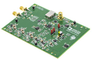
Analog Devices Inc.The LTC2387-16 is a low noise, high speed, 16-bit 15Msps successive approximation register (SAR) ADC ideally suited for a wide range of applications. The combination of excellent linearity and wide dynamic range makes the LTC2387-16 ideal for high speed imaging and instrumentation applications. No-latency operation provides a unique solution for high speed control loop applications. The very low distortion at high input frequencies enables communications applications requiring wide dynamic range and significant signal bandwidth.To support high speed operation while minimizing the number of data lines, the LTC2387-16 features a serial LVDS digital interface. The LVDS interface has one-lane and two-lane output modes, allowing the user to optimize the interface data rate for each application.Applications High Speed Data Acquisition Imaging Communications Control Loops Instrumentation ATE
DC2603A-A
Analog Devices Inc.The LTM4650A is a dual 25A or single 50A output switching mode step-down DC/DC ?Module? (micromodule) regulator with ?1% total DC output error. Included in the package are the switching controllers, power FETs, inductors and all supporting components. Operating from an input voltage range of 4.5V to 16V, the LTM4650A supports two outputs with an output voltage range of 0.6V to 5.5V, each set by a single external resistor. Its high efficiency design delivers up to 25A continuous current for each output. Only a few input and output capacitors are needed. Fast internal control loop compensation allows for fast transient response to minimize output capacitance when powering FPGAs, ASICs, and processors.Fault protection features include overvoltage and overcurrent protection. The LTM4650A is offered in 16mm ? 16mm ? 5.01mm BGA package. LTM4650 Product Family Selection Table VIN Range VOUT Range Compensation DC VOUT Accuracy LTM4650 4.5V to 15V 0.6V to 1.8V Internal 1.5% LTM4650-1B 4.5V to 15V 0.6V to 1.8V External 1.5% LTM4650-1A 4.5V to 15V 0.6V to 1.8V External 0.8% LTM4650A 4.5V to 16V 0.6V to 5.5V Internal 1% LTM4650A-1 4.5V to 16V 0.6V to 5.5V External 1% Applications Telecom and Networking Equipment Storage and ATCA Cards Industrial Equipment
DC2603A-B
Analog Devices Inc.The LTM4650A-1 is a dual 25A or single 50A output switching mode step-down DC/DC ?Module? (micromodule) regulator with ?1% total DC output error. Included in the package are the switching controllers, power FETs, inductors and all supporting components. Operating from an input voltage range of 4.5V to 16V, the LTM4650A-1 supports two outputs with an output voltage range of 0.6V to 5.5V, each set by a single external resistor. Its high efficiency design delivers up to 25A continuous current for each output. Only a few input and output capacitors are needed. Adjustable control loop compensation allows for fast transient response to minimize output capacitance when powering FPGAs, ASICs, and processors.Fault protection features include overvoltage and overcurrent protection. The LTM4650A-1 is offered in 16mm ? 16mm ? 5.01mm BGA package. Vin Range Vout Range Comp DC Vout Accy LTM4650 4.5V to 15V 0.6V to 1.8V Internal 1.5% LTM4650-1B 4.5V to 15V 0.6V to 1.8V External 1.5% LTM4650-1A 4.5V to 15V 0.6V to 1.8V External 0.8% LTM4650A 4.5V to 16V 0.6V to 5.5V Internal 1% LTM4650A-1 4.5V to 16V 0.6V to 5.5V External 1% Applications Telecom and Networking Equipment Storage and ATCA Cards Industrial Equipment
LTC6955/LTC6955-1: Ultralow Jitter 11 Output Fanout Buffer
Analog Devices Inc.Demonstration Circuit 2611A features the LTC6955, Ultralow Jitter 11 Output Fanout Buffers.
By default, the DC2611A is powered from a single 3.3V supply. An option is provided to power to the DC2611A from dual supplies, allowing for the LTC6955’s output supply pins to connect to an LTC Silent Switcher® and the LTC6955 input supply pin to connect to a low noise LDO.
The differential inputs and six of the differential outputs are populated with 0.5" spaced SMA connectors. These outputs are AC-coupled with 50Ω transmission lines making them suitable to drive 50Ω impedance instruments. All registered trademarks and trademarks are the property of their respective owners.
The remaining four differential outputs are terminated with 100Ω.
A calibration path is provided to aid in accurate LTC6955 propagation delay measurements. The calibration path can be also reconfigured as a DC path, which allows for a convenient method of locking the LTC6955 outputs to an external PLL/VCO.
LTM4647 High Efficiency, PolyPhase 120A Step-Down Power μModule Regulator
Analog Devices Inc.Demonstration circuit 2616A-D features a polyphase
design using the LTM4647EY, a 30A high efficiency,
switch mode step-down power µModule regulator. The
input voltage range is from 6V to 15V. To use DC2616A-D
for input voltage range from 4.7V to 6V, connect INTVCC
to SVIN (change R22, R42, R55, R68 from OPT to 0Ω),
DRVCC to VIN (change R21, R38, R52, R65 from 0Ω to
OPT, R2, R39, R53, R66 from OPT to 0Ω). The output voltage range is 0.6V to 1.8V. The DC2616A-D can deliver a
nominal 120A output current with four LTM4647 modules
in parallel. As explained in the data sheet, output current
derating is necessary for certain VIN, VOUT, and thermal
conditions. The board operates in continuous conduction mode in heavy load conditions. For high efficiency at low
load currents, the MODE_PLLIN jumper selects pulseskipping mode for noise sensitive applications or burst
mode operation in less noise sensitive applications. The
MODE_PLLIN pin also allows the LTM4647 to synchronize to an external clock signal. The phase shift between
two adjacent phases is 90 degrees. DC2616A-D has the
option of choosing both internal and external compensation circuit for LTM4647. The LTM4647 data sheet must
be read in conjunction with this demo manual prior to
working on or modifying demo circuit DC2616A-D.
DC2617A
Analog Devices Inc.The LTC6820 provides bidirectional SPI communications between two isolated devices through a single twisted-pair connection. Each LTC6820 encodes logic states into signals that are transmitted across an isolation barrier to another LTC6820. The receiving LTC6820 decodes the transmission and drives the slave bus to the appropriate logic states. The isolation barrier can be bridged by a simple pulse transformer to achieve hundreds of volts of isolation.The LTC6820 drives differential signals using matched source and sink currents, eliminating the requirement for a transformer center tap and reducing EMI. Precision window comparators in the receiver detect the differential signals. The drive currents and the comparator thresholds are set by a simple external resistor divider, allowing the system to be optimized for required cable lengths and desired signal-to-noise performance.Applications Industrial Networking Battery Monitoring Systems Remote Sensors
I2C Programmable Quad Monolithic Boost LED Driver
Analog Devices Inc.The LT3966 is an I2C programmable monolithic boost LED driver with four independent channels. Each channel provides a 60V current mode boost converter with an internal 1.6A DMOS power switch, as well as internal and external analog and PWM dimming features. I2C programmable features include a 13-bit (8192:1) digital PWM generator, 8-bit analog dimming DAC, and flexible fault reporting and handling.An onboard 8-bit ADC allows measurement of each channel?s output voltage and output current, as well as chip input voltage and two external measurements. In addition, independent shutdown and standby control of each channel provides flexible solutions for multitopology applications.The LT3966 is available in a thermally enhanced 6mm ? 6mm 40-Lead QFN package.ApplicationsBacklightingHeads Up Displays
LTM4678 Demo Board | Dual 25A or Single 50A μModule Regulator with Digital Power System Management 2x LTM4678; 100A
Analog Devices Inc.Demonstration circuit 2638A-A is a high efficiency, high density, μModule regulator with 4.5V to 16V input range. The output voltage is adjustable from 0.5V to 3.3V, and it can supply 100A maximum load current. The demo board has two LTM4678 μModule® regulators, and the LTM4678 is a dual 25A or single 50A step-down regulator with PMBus power system management. Please see LTM4678 data sheet for more detailed information.
DC2638A-A powers up to default settings and produce power based on configuration resistors without the need for any serial bus communication. This allows easy evaluation of the DC/DC converter. To fully explore the extensive power system management features of the part, download the GUI software LTpowerPlay® onto your PC and use ADI’s I2C/SMBus/PMBus dongle DC1613A to connect to the board. LTpowerPlay allows the user to reconfigure the part on-the-fly and store the configuration in EEPROM, view telemetry of voltage, current, temperature and fault status.
GUI Download: The software can be downloaded from: LTpowerPlay.
For more details and instructions of LTpowerPlay, please refer to LTpowerPlay GUI for LTM4678 Quick Start Guide.
LTM4678 Demo Board | Dual 25A or Single 50A μModule Regulator with Digital Power System Management 5x LTM4678; 250A
Analog Devices Inc.Demonstration circuit 2638A-D is a high efficiency, high density, μModule regulator with 4.5V to 16V input range. The output voltage is adjustable from 0.5V to 3.3V, and it can supply 250A maximum load current. The demo board has five LTM4678 μModule® regulators, and the LTM4678 is a dual 25A or single 50A step-down regulator with PMBus power system management. Please see LTM4678 data sheet for more detailed information.
DC2638A-D powers up to default settings and produce power based on configuration resistors without the need for any serial bus communication. This allows easy evaluation of the DC/DC converter. To fully explore the extensive power system management features of the part, download the GUI software LTpowerPlay® onto your PC and use ADI’s I2C/SMBus/PMBus dongle DC1613A to connect to the board. LTpowerPlay allows the user to reconfigure the part on-the-fly and store the configuration in EEPROM, view telemetry of voltage, current, temperature and fault status.
GUI Download: The software can be downloaded from: LTpowerPlay.
For more details and instructions of LTpowerPlay, please refer to LTpowerPlay GUI for LTM4678 Quick Start Guide.
LTC1628CG | Multi-Phase, 3 Output Regulator, 7-28VIN; 5V @ 3A, 3.3V @ 4A and a Linear 12V @ 150mA
Analog Devices Inc.DC264A: Demo Board for the LTC1628 High Efficiency, 2-Phase Synchronous Step-Down Switching Regulator.
DC2655A-A
Analog Devices Inc.The LTC6363 family consists of four fully differential, low power, low noise amplifiers with rail-to-rail outputs optimized to drive SAR ADCs. The LTC6363 is a standalone differential amplifier, where the gain is typically set using four external resistors. The LTC6363-0.5, LTC6363-1, and LTC6363-2 each have internal matched resistors to create fixed gain blocks with gains of 0.5V/V, 1V/V, and 2V/V respectively. Each of the fixed-gain amplifiers features precision laser trimmed on-chip resistors for accurate, ultrastable gain and excellent CMRR.Applications 20-Bit, 18-Bit and 16-Bit SAR ADC Drivers Single-Ended-to-Differential Conversion Low Power ADC Drivers Level Shifter Differential Line Drivers Battery-Powered Instrumentation
LTC1628CG | Multi-Phase, 3 Output Regulator, 7-28VIN; 5V @ 3A, 3.3V @ 4A and a Synchronous 12V @ 200mA
Analog Devices Inc.DC265A: Demo Board for the LTC1628 High Efficiency, 2-Phase Synchronous Step-Down Switching Regulator.
DC2665A-B
Analog Devices Inc.The LTM4638 is a complete 15A step-down switching mode ?Module (power module) regulator in a tiny 6.25mm ? 6.25mm ? 5.02mm BGA package. Included in the package are the switching controller, power FETs, inductor and support components. Operating over an input voltage range of 3.1V to 20V, the LTM4638 supports an output voltage range of 0.6V to 5.5V, set by a single external resistor. Its high efficiency design delivers up to 15A continuous output current. Only bulk input and output capacitors are needed.The LTM4638 supports selectable discontinuous mode operation and output voltage tracking for supply rail sequencing. Its high switching frequency and current mode control enable a very fast transient response to line and load changes without sacrificing stability.Fault protection features include overvoltage, overcurrent and overtemperature protection.The LTM4638 is available with SnPb or RoHS compliant terminal finish.APPLICATIONS Telecom, Datacom, Networking and Industrial Equipment Medical Diagnostic Equipment Data Storage Rack Units and Cards Test and Debug Systems
DC2666A-B
Analog Devices Inc.The LTC7132 is a dual output PolyPhase DC/DC synchronous step-down monolithic regulator with an I2C-based PMBus compliant serial interface. The regulator employs a constant-frequency current mode architecture, together with a unique scheme to provide excellent performance in sub-milliohm DCR applications. The LTC7132 is supported by the LTpowerPlay? software development tool with graphical user interface (GUI).Programmable loop compensation allows the regulator to be compensated digitally. The switching frequency, channel phasing and device address can be programmed both by the digital interface as well as the external configuration resistors. Additionally, parameters can be set via the digital interface and stored in EEPROM. Both outputs have independent power good indicators and FAULT function.The LTC7132 can be configured to operate in discontinuous (pulse-skipping) mode or forced continuous conduction mode. Each channel can deliver up to 25A of loadcurrent; the total current capability will depend on the APPLICATIONS total power dissipations on both channels.POWER CONVERSION Wide VIN Range: 4.5V to 20V VOUT Range: 0.5V to 3.5V (with Ultralow DCR Setting); 0.5V to 5.5V (Typical DCR Setting) Accurate PolyPhase? Current Sharing for Up to 6 Phases Available in a 140-Lead (9mm ? 11.25mm ? 2.22mm) BGA PackageAPPLICATIONS Telecom, Datacom and Storage Systems Industrial and Point-of-Load Applications
LTC1562CG-2 | Very-Low-Noise, Low Distortion Quad Universal Filter
Analog Devices Inc.Demonstration circuit DC266B-A is for the evaluation of 8th order filter circuits using an LTC1562 (no dash) and DC266B-B for an LTC1562-2. LTC1562 and LTC1562-2 are quad 2nd order active-RC filter building blocks. Each 2nd order section has an integrator trimmed with internal capacitors and resistors to 100kHz and 200 kHz for the LTC1562 and LTC1562-2 respectively. The trimmed frequency error is ±0.6% for the LTC1562A and ±1.5% for the LTC1562-2. The LTC1562 or LTC1562-2 2nd order sections can be configured with external resistors to implement lowpass, bandpass or highpass filters.
LTM4664 Demo Board | 48VIN, Dual 25A μModule Regulator With Digital Power System Management
Analog Devices Inc.Demonstration circuit 2672A-A is a complete non-isolated 48V input, dual-output, high efficiency, high density µModule regulator with 30V to 58V input range. Each output can supply 25A maximum load current. The demo board has a LTM4664 µModule regulator, which is a dual 25A or single 50A step-down regulator with digital power system management. Please see the LTM4664 datasheet for more detailed information.
DC2672A-A powers up to default settings and produces power based on configuration resistors without the need for any serial bus communication. This allows easy evaluation of the DC/DC converter. To fully explore the extensive power system management features of the part, download the GUI software LTpowerPlay™ onto your PC and use ADI’s I2C/SMBus/PMBus dongle DC1613A to connect to the board. LTpowerPlay allows the user to reconfigure the part on the fly and store the configuration in EEPROM, view telemetry of voltage, current, temperature and fault status.
LTC4418 Dual Channel Prioritized PowerPath Controller
Analog Devices Inc.Demonstration circuit 2707B uses the LTC®4418 to arbitrate between two input supply rails, selecting the highest priority, valid supply to power the load. The V1 rail is defined to have higher priority and the V2 rail has lower priority. Both rails have individual overvoltage and undervoltage comparators for setting valid window thresholds with external resistive dividers. If the highest priority rail voltage V1 falls out of the defined window (overvoltage or undervoltage), the V2 rail, if it is valid, is enabled and powers
the load. Two or more LTC4418s can be cascaded to provide switchover between more than two rails.
DC270A
Analog Devices Inc.The LTC1772 is a constant frequency current mode step-down DC/DC controller providing excellent AC and DC load and line regulation. The device incorporates an accurate undervoltage lockout feature that shuts down the LTC1772 when the input voltage falls below 2.0V.The LTC1772 provides a ?2.5% output voltage accuracy and consumes only 270?A of quiescent current. For applications where efficiency is a prime consideration, the LTC1772 is configured for Burst Mode operation, which enhances efficiency at low output current. To further maximize the life of a battery source, the external P-channel MOSFET is turned on continuously in dropout (100% duty cycle).In shutdown, the device draws a mere 8?A. High constant operating frequency of 550kHz allows the use of a small external inductor.The LTC1772 is available in a small footprint 6-lead SOT-23. Burst Mode LTC1772 Yes LTC1772B No Applications One or Two Lithium-Ion-Powered Applications Cellular Telephones Wireless Modems Portable Computers Distributed 3.3V, 2.5V or 1.8V Power Systems Scanners
LT8316 Demo Board | Isolated Flyback Converter: 100V to 600VIN, VOUT = 12V @ Up to 3A
Analog Devices Inc.Demonstration circuit 2718A is a no-opto flyback converter featuring the LT8316. The demo board outputs 12V and maintains tight regulation with a load current from 30mA to 3A. It is optimized to operate over a wide 100V to 600V DC input voltage range. Output voltage accuracy stays within ±5% over the entire input voltage and load range.
The LT8316 is a high voltage flyback controller. No optoisolator is needed for regulation. The part samples the output voltage from the isolated flyback waveform appearing across a third winding on the transformer. Quasi-resonant boundary mode operation improves load regulation. The LT8316 is available in a thermally enhanced 20-pin TSSOP package with four pins removed for high-voltage spacing.
The LT8316 data sheet gives a complete description of the part, operation and application information. The data sheet must be read in conjunction with this quick start guide for demo circuit 2718A.
3.3V VIN, Dual 2A, 6MHz Synchronous Step-Down Regulators at 1.8V and 2.0V Outputs, in a 0.71cm2 Solution
Analog Devices Inc.Demonstration Circuit DC2748A features the LTC3315B dual 5V, 2A Synchronous Step-Down DC/DC regulators operating at 6MHz. One regulator provides a 1.8V output
and the other provides 2.0V, both up to a 2A load. The LTC3315B supports adjustable output voltages from 0.5V to VIN, operating frequencies from 3MHz up to 10MHz. The LTC3315B is a compact, high efficiency, and high speed synchronous monolithic step-down switching regulator. Fast minimum on-time of 25ns enables high
VIN to low VOUT conversion at high frequency.
The DC2748A operating mode may be selected as Burst Mode operation, Skip mode or Forced Continuous (FC) mode. Setting JP1 to the FC/SYNC position will allow the
LTC3315B to sync to a clock frequency from 3MHz to 10MHz. The LTC3315B operates in Forced Continuous mode when syncing to an external clock.
The LTC3315B data sheet gives a complete description of the device, operation and application information. The data sheet must be read in conjunction with the demo manual. The LTC3315B is assembled in a 2mm × 2mm LQFN package with exposed pads for low thermal resistance. The PCB Considerations section in the data sheet.
The Efficiency vs Load graph on the demo manual shows the efficiency and the power loss of the circuit with a 3.3V input in Burst Mode operation.


