
EVAL-ADF7025DBZ1
Analog Devices Inc.The ADF7025 is a low power, highly integrated FSK transceiver. It is designed for operation in the license?free ISM bands of 433 MHz, 862 MHz to 870 MHz, and 902 MHz to 928 MHz. The ADF7025 can be used for applications operating under the European ETSI EN300-220 or the North American FCC (Part 15) regulatory standards. The ADF7025 is intended for wideband, high data rate applications with deviation frequencies from 100 kHz to 750 kHz and data rates from 9.6 kbps to 384 kbps. A complete transceiver can be built using a small number of external discrete components, making the ADF7025 very suitable for price-sensitive and area-sensitive applications.The ADF7025 transceiver is suitable for operation under FCC 15.247 Digital Modulation Specification characterized by large deviation frequencies. This allows up to 1Watt transmit power without the need to frequency hop, thereby significantly reducing protocol overhead.APPLICATIONS Wireless audio/video Remote control/security systems Wireless metering Keyless entry Home automation

EVAL-ADF7030DB7Z
Analog Devices Inc.The ADF7030 is a low power, high performance, integrated radio transceiver supporting narrowband operation in the 169.4MHz to 169.6MHz ISM bands. The ADF7030 supports transmit and receive operation at 2.4kbps and 4.8kbps using 2GFSK modulation and transmit operation at 6.4kbps using 4GFSK modulation.The ADF7030 features an on-chip ARM? Cortex?-M0 processor that performs radio control and packet management.Applications Wireless M-Bus Mode N (EN 13757-4) Smart metering Social alarms Active tag asset tracking

EVAL-ADF7242DB1Z
Analog Devices Inc.The ADF7242 is a highly integrated, low power, and high performance transceiver for operation in the global 2.4 GHz ISM band. It is designed with emphasis on flexibility, robustness, ease of use, and low current consumption. The IC supports the IEEE 802.15.4-2006 2.4 GHz PHY requirements as well as proprietary GFSK/ FSK/GMSK/MSK modulation schemes in both packet and data streaming modes. With a minimum number of external components, it achieves compliance with the FCC CFR47 Part 15, ETSI EN 300 440 (Equipment Class 2), ETSI EN 300 328 (FHSS, DR > 250 kbps), and ARIB STD T-66 standards.The ADF7242 complies with the IEEE 802.15.4-2006 2.4 GHz PHY requirements with a fixed data rate of 250 kbps and DSSS-OQPSK modulation. With its support of GFSK/FSK/GMSK/MSK modulation schemes, the IC can operate over a wide range of data rates from 50 kbps to 2 Mbps and is, therefore, equally suitable for proprietary applications in the areas of smart metering, industrial control, home and building automation, and consumer electronics. In addition, the agile frequency synthesizer of the ADF7242, together with short turnaround times, facilitates the implementation of FHSS systems.The transmitter path of the ADF7242 is based on a direct closed-loop VCO modulation scheme using a low noise fractional-N RF frequency synthesizer. The automatically calibrated VCO operates at twice the fundamental frequency to reduce spurious emissions and avoid PA pulling effects. The bandwidth of the RF frequency synthesizer is automatically optimized for transmit and receive operations to achieve optimum phase noise, modulation quality, and synthesizer settling time performance. The transmitter output power is programmable from ?20 dBm to +4 dBm with automatic PA ramping to meet transient spurious specifications. An integrated biasing and control circuit is available in the IC to significantly simplify the interface to external PAs.The receive path is based on a zero-IF architecture enabling very high blocking resilience and selectivity performance, which are critical performance metrics in interference dominated environments such as the 2.4 GHz band. In addition, the architecture does not suffer from any degradation of blocker rejection in the image channel, which is typically found in low IF receivers. In GFSK/FSK modes, the receiver features a high speed automatic frequency control (AFC) loop, which allows the frequency synthesizer to find and correct any frequency errors in the received packet.The IC can operate with a supply voltage between 1.8 V and 3.6 V with very low power consumption in receive and transmit modes while maintaining its excellent RF performance, making it especially suitable for battery-powered systems.The ADF7242 features a flexible dual-port RF interface that can be used with an external LNA and/or PA in addition to supporting switched antenna diversity.The ADF7242 incorporates a very low power custom 8-bit processor that supports a number of transceiver management functions. These functions are handled by the two main modules of the processor; the radio controller and the packet manager.See data sheet for additional information.APPLICATIONS Wireless sensor networks Automatic meter reading/Smart metering Industrial wireless control Healthcare Wireless audio/video Consumer electronics Zigbee
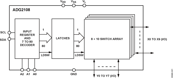
EVAL-ADG2108EBZ
Analog Devices Inc.The ADG2108?is an analog cross point switch with anarray size of 8 ? 10. The switch array is arranged so that there are eight columns by 10 rows, for a total of 80 switchchannels. The array is bidirectional, and the rows and columns can be configured as either inputs or outputs. Each of the 80switches can be addressed and configured through the I2C compatible interface. Standard, full speed, and high speed (3.4 MHz) I2C interfaces are supported. Any simultaneous switch combination is allowed. An additional feature of the ADG2108 is that switches can be updated simultaneously,using the LDSW command. In addition, a RESET option allows all of the switch channels to be reset/off. At power on, all switches are in the off condition. The device is packaged in a 32-lead, 5 mm ? 5 mm LFCSP_VQ.APPLICATIONS AV Switching in TV Automotive Infotainment AV Receivers CCTV Ultrasound Applications KVM Switching Telecom Applications Test Equipment/Instrumentation PBX Systems

EVAL-ADG5421FEBZ
Analog Devices Inc.The ADG5421F is a dual SPST, low on resistance switch that features overvoltage protection, power-off protection, and overvoltage detection on the source pins. When no power supplies are present, the switch remains in the off condition, and the switch inputs are high impedance. When powered, if the analog input signal levels on either of the Sx pins exceed VDD or VSS by the threshold voltage, VT, both switches turn off together, and the open-drain fault flag (FF) pin pulls to a logic low. Input signal levels up to +60 V or ?60 V relative to ground are blocked in both the powered and unpowered condition. The switches turn on with a Logic 1 input and conduct equally well in both directions. The digital input is compatible with 1.8 V logic inputs over the full operating supply range. APPLICATIONS Analog input and output modulesProcess control and distributed control systemsData acquisitionInstrumentationAvionicsAutomatic test equipmentCommunication systemsRelay replacement
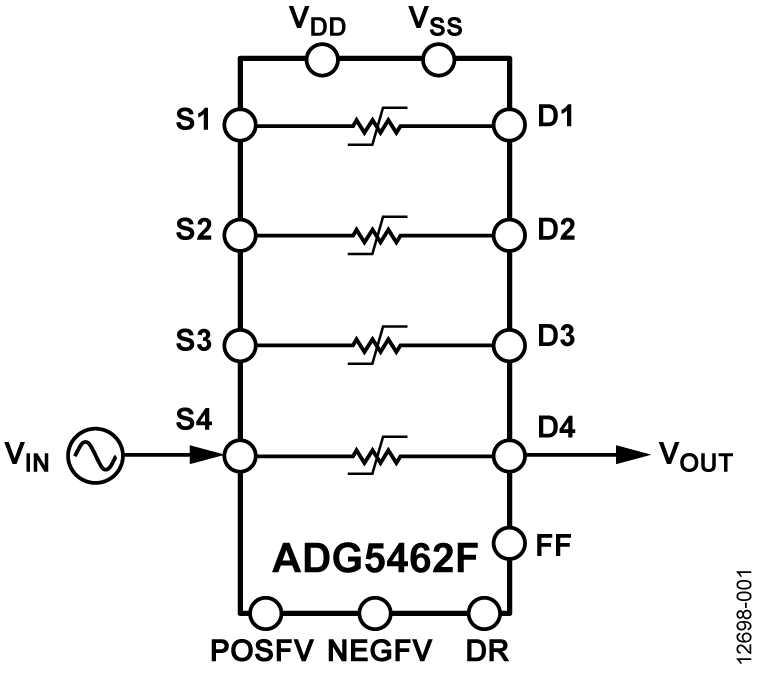
EVAL-ADG5462FEBZ
Analog Devices Inc.The ADG5462F contains four channels that are overvoltage protected. The channel protector is placed in series with the signal path and protects sensitive components from overvoltage faults in that path. The channel protector prevents overvoltages when powered and unpowered, and it is ideal for use in applications where correct power supply sequencing cannot always be guaranteed. The primary supply voltages define the on-resistance profile, while the secondary supply voltages define the voltage level at which the overvoltage protection engages.When no power supplies are present, the channel remains in the off condition, and the channel inputs are high impedance. Under normal operating conditions, if the analog input signal levels on any Sx pin exceed positive fault voltage (POSFV) or negative fault voltage (NEGFV) by a threshold voltage (VT), the channel turns off and that Sx pin becomes high impedance. If the DR pin is driven low, the drain pin (Dx) is pulled to the secondary supply voltage that was exceeded. The output profile for each DR voltage level is shown in Figure 1. Input signal levels up to ?55 V or +55 V relative to ground are blocked in both the powered and unpowered conditions.The low on-resistance of these switches, combined with the on-resistance flatness over a significant portion of the signal range make them an ideal solution for data acquisition and instrumentation applications where excellent linearity and low distortion are critical.Product Highlights Source pins are protected against voltages greater than the secondary supply rails (POSFV and NEGFV), up to ?55 V and +55 V. In an unpowered state, source pins (Sx) are protected against voltages from ?55 V to +55 V. Overvoltage detection with digital output indicates operating state of channel. Trench isolation guards against latch-up. Optimized for low on-resistance and on-resistance flatness. The ADG5462F operates from a dual power supply range of ?5 V to ?22 V or a single power supply range of 8 V to 44 V.Applications Analog input/output modules Process control/distributed control systems Data acquisition Instrumentation Avionics Automatic test equipment Communication systems

EVAL-ADG7421FEBZ
Analog Devices Inc.The ADG7421F is a low voltage, dual single-pole/single-throw (SPST), low on-resistance switch that features overvoltage protection, power-off protection, and overvoltage detection on the source pins.When no power supplies are present, the switch remains in the off condition, and the switch inputs are high impedance. When powered, if the analog input signal levels on the Sx pins exceed VDD or VSS by a threshold voltage, VT, the switch automatically turns off and the digital FF (fault flag) pin drops to a logic low to indicate a fault.Input signal levels up to +60 V or ?60 V relative to ground are blocked, in both the powered and unpowered condition. The switches turn on with a Logic 1 input and conducts equally well in both directions with an analog signal range of VSS + 0.1 V to VDD ? 0.55 V for a 5 V single supply. The digital input is compatible with 1.8 V logic inputs over the full operating supply range.The ADG7421F is ideal for providing overvoltage protection for small signals such as resistance temperature device (RTD) inputs (see Figure 56 in the data sheet) and thermocouple inputs (see Figure 55). The ability to protect against high voltages up to ?60 V coupled with a low voltage supply can enable complete low voltage input stages for industrial applications.APPLICATIONS Analog input/output modules Process control/distributed control systems? Data acquisition? Instrumentation? Avionics? Automatic test equipment? Communication systems Relay replacement

EVAL-ADG884EBZ
Analog Devices Inc.The ADG884 is a low voltage CMOS device containing two independently selectable single-pole, double-throw (SPDT) switches. This device offers ultralow on resistance of 0.41 ? over the full temperature range, making the part an ideal solution for applications that require minimal distortion through the switch. The ADG884 also has the capability of carrying large amounts of current, typically 600 mA at 5 V operation.The ADG884 is available in a 10-ball, 2 mm ? 1.5 mm WLCSP package, a 10-lead LFCSP_WD package, and a 10-lead MSOP package. These tiny packages make the ADG884 the ideal solution for space-constrained applications.When on, each switch conducts equally well in both directions and has an input signal range that extends to the supplies. The ADG884 exhibits break-before-make switching action.Product Highlights Single 1.8 V to 5.5 V operation. High current handling capability (400 mA continuous current). 1.8 V logic compatible. Low THD + N (0.01% typical). Tiny 2 mm ? 1.5 mm WLCSP, 3 mm ? 3 mm 10-lead LFCSP_WD, and 10-lead MSOP packages. ApplicationsCellular phonesPDAsMP3 playersPower routingBattery-powered systemsPCMCIA cardsModemsAudio and video signal routingCommunications systemsData Sheet, Rev. C, 6/08

EVAL-ADG888EBZ
Analog Devices Inc.The ADG888 is a low voltage, dual DPDT (double-pole,double-throw) CMOS device optimized for high performanceaudio switching. With its low power and small physical size, it isideal for portable devices.This device offers ultralow on resistance of less than 0.8 ? overthe full temperature range, making it an ideal solution forapplications requiring minimal distortion through the switch.The ADG888 also has the capability of carrying large amountsof current, typically 400 mA at 5 V operation.When on, each switch conducts equally well in both directionsand has an input signal range that extends to the supplies. TheADG888 exhibits break-before-make switching action.The ADG888 is available in a 16-ball WLCSP, 16-lead LFCSP,and a 16-lead TSSOP. These packages make the ADG888 the ideal solution for space-constrained applications.Product Highlights

EVAL-ADG936REBZ
Analog Devices Inc.The ADG936 / ADG936-R are wideband analog switches that comprise two independently selectable SPDT switches using a CMOS process to provide high isolation and low insertion loss to 1 GHz. The ADG936 is an absorptive/matched dual SPDT with 50 ? terminated shunt legs; the ADG936-R is a reflective dual SPDT. These devices are designed such that the isolation is high over the dc to 1 GHz frequency range. They have on-board CMOS control logic, eliminating the need for external controlling circuitry. The control inputs are both CMOS and LVTTL compatible. The low power consumption of these CMOS devices makes them ideally suited for wireless applications and general-purpose high frequency switching.

EVAL-ADHV4702-1CPZ
Analog Devices Inc.The ADHV4702-1 is a high voltage (220 V), unity-gain stable precision operational amplifier. The ADHV4702-1 offers high input impedance with low input bias current, low input offset voltage, low drift, and low noise for precision demanding applications. The next generation of proprietary semiconductor processes and innovative architecture from Analog Devices, Inc., enable this precision operational amplifier to operate from symmetrical dual supplies of ?110 V, asymmetrical dual supplies, or a single supply of 220 V. The ADHV4702-1?requires a minimum supply voltage of ?12 V from the?reference voltage for normal operation.For precision performance, the ADHV4702-1 has a 170 dB typical open-loop gain (AOL) and a 160 dB typical common-mode rejection ratio (CMRR). The ADHV4702-1 also has a 2 ?V/?C maximum input offset voltage (VOS) drift and an 8 nV/?Hz input voltage noise.The exceptional dc precision of the ADHV4702-1 is complemented by excellent dynamic performance with a small signal bandwidth of 10 MHz and a slew rate of 74 V/?s. The ADHV4702-1 has an output current of 20 mA typical.The ADHV4702-1 offers high voltage input common-mode swing as well as high voltage output swing, enabling precision high voltage use cases such as high-side current sensing. The ADHV4702-1 is also ideally suited for forcing a voltage in precision bias and control applications.The ADHV4702-1 is available in a 12-lead, 7 mm ? 7 mm lead frame chip scale package (LFCSP) with an exposed pad (EPAD) compliant to international electrotechnical commission (IEC) 61010-1 creepage and clearance standards. The copper EPAD provides a low thermal resistance path to improve heat dissipation and features high voltage isolation, allowing it to be safely connected to a 0 V ground plane regardless of VCC or VEE voltages. The ADHV4702-1 operates over the ?40?C to +85?C industrial temperature range.Applications High-side current sensing Automated test equipment High voltage drivers Piezotransducers Digital-to-analog converter (DAC) output buffers Light detecting and ranging (LiDAR), avalanche photodiode (APD), single photon avalanche diode (SPAD) biasing

EVAL-ADM1060EBZ
Analog Devices Inc.The ADM1060?is a programmable supervisory/sequencing device that offers a single chip solution for multiple power supply fault detection and sequencing in communications systems.In central offices, servers, and other infrastructure systems, a common backplane dc supply is reduced to multiple board supplies using dc-to-dc converters. These multiple supplies are used to power different sections of the board, such as 3.3 V logic circuits, 5 V logic circuits, DSP core, and DSP I/O circuits. There is usually a requirement that certain sections power up before others; for example, a DSP core may need to power up before the DSP I/O, or vice versa, to avoid damage, miscommunication, or latch-up. The ADM1060 facilitates this, providing supply fault detection and sequencing/combinatorial logic for up to seven independent supplies. The seven supply fault detectors consist of one high voltage detector (up to +14.4 V), two bipolar voltage detectors (up to +6 V or down to ?6 V), and four positive low voltage detectors (up to +6 V). All of the detectors can be programmed to detect undervoltage, overvoltage, or out-ofwindow (undervoltage or overvoltage) conditions. The inputs to these supply fault detectors are via the VH (high voltage) pin, VBn (positive or negative) pins, and VPn (positive only) pins. Either the VH supply or one of the VPn supplies is used to power the ADM1060 (whichever is highest). This ensures that in the event of a supply failure, the ADM1060 is kept alive for as long as possible, thus enabling a reliable fault flag to be asserted and the system to be powered down in an ordered fashion.Other inputs to the ADM1060 include a watchdog detector (WDI) and four general-purpose inputs (GPIn). The watchdog detector can be used to monitor a processor clock. If the clock does not toggle (transition from low to high or from high to low) within a programmable timeout period (up to 18 sec.), a fail flag will assert. The four general-purpose inputs can be configured as logic buffers or to detect positive/negative edges and to generate a logic pulse or level from those edges. Thus, the user can input control signals from other parts of the system (e.g., RESET or POWER_GOOD) to gate the sequencing of the supplies supervised by the ADM1060.The ADM1060 features nine programmable driver outputs (PDOs). All nine outputs can be configured to be logic outputs, which can provide multiple functions for the end user such as RESET generation, POWER_GOOD status, enabling of LDOs, and watchdog timeout assertion. PDOs 1 to 4 have the added feature of being able to provide an internally charge-pumped high voltage for use as the gate drive of an external N-channel FET that could be placed in the path of one of the supplies being supervised.APPLICATIONS Central office systems Servers Infrastructure network boards High density, multivoltage system cards

EVAL-ADM1069LQEBZ
Analog Devices Inc.The ADM1069 Super Sequencer? is a configurable supervisory/sequencing device that offers a single-chip solution for supplymonitoring and sequencing in multiple supply systems. In additionto these functions, the ADM1069 integrates a 12-bit analog-todigitalconverter (ADC) and four 8-bit voltage output digital-toanalogconverters (DACs). These circuits can implement a closedloopmargining system that enables supply adjustment by alteringeither the feedback node or reference of a dc-to-dc converterusing the DAC outputs.For more information about the ADM1069 register map, referto the AN-721 Application Note.Applications Central office systems Servers/routers Multivoltage system line cards DSP/FPGA supply sequencing In-circuit testing of margined supplies

EVAL-ADM1073MEBZ
Analog Devices Inc.The ADM1073 is a full-feature, negative voltage, hot swap controller that allows boards to be safely inserted and removed from a live ?48 V backplane. The part provides precise and robust current limiting, and protection against both transient and nontransient short circuits in overvoltage and undervoltage conditions. The ADM1073 can operate from a negative voltage of ?18 V to ?80 V and can tolerate transient voltages of up to ?200 V.Inrush current is limited to a programmable value by control-ling the gate drive of an external N-channel FET. The maximum current limit is set by the choice of the sense resistor, RSENSE.A built-in soft start function allows control of the inrush current profile by an external capacitor on the soft start (SS) pin.An external capacitor on the TIMER pin determines the time for which the FET gate is controlled to be high when maximum inrush current flows. The ADM1073 employs a limited consecutive retry scheme, whereby, if the load capacitance is not fully charged within one attempt, the FET gate is pulled low and retries after a cooling period.APPLICATIONS Central office switching Telecommunication and data communication equipment ?48 V distributed power systems Negative power supply control High availability servers ?48 V power supply modules Disk arrays

EVAL-ADM1175EBZ
Analog Devices Inc.The ADM1175 is an integrated hot swap controller and current sense amplifier that offers digital current and voltage monitoring via an on-chip, 12-bit analog-to-digital converter (ADC), communicated through an I2C interface.An internal current sense amplifier senses voltage across the sense resistor in the power path via the VCC pin and the SENSE pin.The ADM1175 limits the current through this resistor by controlling the gate voltage of an external N-channel FET in the power path, via the GATE pin. The sense voltage (and, therefore, the inrush current) is kept below a preset maximum.The ADM1175 protects the external FET by limiting the time that it spends with maximum current running through it. This current limit period is set by the choice of capacitor attached to the TIMER pin. Additionally, the device provides protection from overcurrent events that may occur once the hot swap event is complete. In the case of a short-circuit event, the current in the sense resistor exceeds an overcurrent trip threshold, and the FET is switched off immediately by pulling down the GATE pin.A 12-bit ADC can measure the current seen in the sense resistor, as well as the supply voltage on the VCC pin. An industry-standard I2C interface allows a controller to read current and voltage data from the ADC. Measurements can be initiated by an I2C command or via the convert (CONV) pin. The CONV pin is especially useful for synchronizing reads on multiple ADM1175 devices. Alternatively, the ADC can run continuously, and the user can read the latest conversion data whenever it is required. Up to four unique I2C addresses can be created, depending on the way the ADR pin is connected.The ADM1175 is packaged in a 10-lead MSOP.Applications Power monitoring/power budgeting Central office equipment Telecommunication and data communication equipment PCs/servers

EVAL-ADM1185EBZ
Analog Devices Inc.The ADM1185 is an integrated, 4-channel, voltage monitoring and sequencing device. A 2.7 V to 5.5 V power supply is required on the VCC pin to power the device.Four precision comparators monitor four voltage rails. All comparators have a 0.6 V reference with a worst-case accuracy of 0.8%. Resistor networks that are external to the VIN1, VIN2, VIN3, and VIN4 pins set the trip points for the monitored supply rails.A digital core interprets the status of the comparator outputs.Internal time delays can be used for sequencing the startup of subsequent power supplies enabled by the outputs. Supplies falling out of range are also detected and, as a result, appropriate outputs are disabled.The ADM1185 has four open-drain outputs. In a typical configuration, OUT1 to OUT3 are used to enable power supplies, while PWRGD is a common power-good output, indicating the status of all monitored supplies.The ADM1185 is available in a 10-lead mini small outline package (MSOP).APPLICATIONS Monitor and alarm functions Power supply sequencing Telecommunication and data communication equipment PCs/servers

EVAL-ADM1186-1EBZ
Analog Devices Inc.The ADM1186-1 and ADM1186-2 are integrated, four-channel, voltage monitoring and sequencing devices. A 2.7 V to 5.5 V power supply is required on the VCC pin for power.Four precision comparators monitor four voltage rails, with all comparators sharing a 0.6 V reference and a worst-case accuracy of 0.8%. Resistor networks that are external to the VIN1, VIN2, VIN3, and VIN4 pins set the Under Voltage (UV) trip points for the monitored supply rails.The ADM1186-1 and ADM1186-2 have four open drain enable outputs, OUTx, that are used to enable power supplies. An open drain power good output, PWRGD, is provided that indicatesthe four VINx inputs are above their UV thresholds.A state machine monitors the state of the UP and?DOWN pins on the ADM1186-1 or the UP/overbar: DOWN pin on the ADM1186-2 to control the supply sequencing direction. In the ?Wait Start?state, a rising edge transition on the UP or UP/DOWN pin triggers a power-up sequence. A falling edge transition on the DOWN or UP/DOWN pin in the ?Power Up Done? statetriggers a power down sequence.During a power up sequence, the state machine enables each power supply in turn. The supply output voltage is monitored to determine if it rises above the UV threshold level within a userdefined duration called the blanking time. If a supply rises above the UV threshold then the next enable output in the sequence is turned on. In addition to the blanking time a user may also define sequencing time delays between each enable output turning on. When all four enable outputs are on, and the four VINx pins are above their UV trip points the power up sequence is complete. The ADM1186-1 provides an open drain pin, SEQ_DONE, that is asserted high to provide an indication that an up sequence is complete. The SEQ_DONE pins is allows multiple cascadedADM1186-1 devices to be perform controlled power up and down sequences. During a power down sequence the enable outputs turn off inreverse order. The sequence time delays between successive supplies the same as during the power up sequence, and no blanking time is used during a power down sequence. At the end of a down sequence the SEQ_DONE pin is brought low. During sequencing and when powered up, the state machine continuously monitors for any fault conditions. Faults include a UV condition on any of the inputs, or an unexpected controlinput. Any fault that occurs causes the state machine to enter a fault handler. This immediately turns off all enable outputs, and ensures that the device is ready to start a new up sequence. The ADM1186-1 has a bi-directional open drain pin, FAULT, that facilitates fault handling when using multiple devices. An ADM1186-1 experiencing a fault condition drives the FAULT pin low, causing other connected ADM1186-1devices to enter their own fault handling state.The ADM1186-1 is available in a 20-lead QSOP package andthe ADM1186-2 is available in a 16-lead QSOP package.
EVAL-ADM1186-2EBZ
Analog Devices Inc.The ADM1186-1 and ADM1186-2 are integrated, four-channel, voltage monitoring and sequencing devices. A 2.7 V to 5.5 V power supply is required on the VCC pin for power.Four precision comparators monitor four voltage rails, with all comparators sharing a 0.6 V reference and a worst-case accuracy of 0.8%. Resistor networks that are external to the VIN1, VIN2, VIN3, and VIN4 pins set the Under Voltage (UV) trip points for the monitored supply rails.The ADM1186-1 and ADM1186-2 have four open drain enable outputs, OUTx, that are used to enable power supplies. An open drain power good output, PWRGD, is provided that indicatesthe four VINx inputs are above their UV thresholds.A state machine monitors the state of the UP and?DOWN pins on the ADM1186-1 or the UP/overbar: DOWN pin on the ADM1186-2 to control the supply sequencing direction. In the ?Wait Start?state, a rising edge transition on the UP or UP/DOWN pin triggers a power-up sequence. A falling edge transition on the DOWN or UP/DOWN pin in the ?Power Up Done? statetriggers a power down sequence.During a power up sequence, the state machine enables each power supply in turn. The supply output voltage is monitored to determine if it rises above the UV threshold level within a userdefined duration called the blanking time. If a supply rises above the UV threshold then the next enable output in the sequence is turned on. In addition to the blanking time a user may also define sequencing time delays between each enable output turning on. When all four enable outputs are on, and the four VINx pins are above their UV trip points the power up sequence is complete. The ADM1186-1 provides an open drain pin, SEQ_DONE, that is asserted high to provide an indication that an up sequence is complete. The SEQ_DONE pins is allows multiple cascadedADM1186-1 devices to be perform controlled power up and down sequences. During a power down sequence the enable outputs turn off inreverse order. The sequence time delays between successive supplies the same as during the power up sequence, and no blanking time is used during a power down sequence. At the end of a down sequence the SEQ_DONE pin is brought low. During sequencing and when powered up, the state machine continuously monitors for any fault conditions. Faults include a UV condition on any of the inputs, or an unexpected controlinput. Any fault that occurs causes the state machine to enter a fault handler. This immediately turns off all enable outputs, and ensures that the device is ready to start a new up sequence. The ADM1186-1 has a bi-directional open drain pin, FAULT, that facilitates fault handling when using multiple devices. An ADM1186-1 experiencing a fault condition drives the FAULT pin low, causing other connected ADM1186-1devices to enter their own fault handling state.The ADM1186-1 is available in a 20-lead QSOP package andthe ADM1186-2 is available in a 16-lead QSOP package.

EVAL-ADM1260EBZ
Analog Devices Inc.The ADM1260 Super Sequencer? is a configurable supervisory/sequencing device that offers a single-chip solution for supply monitoring and sequencing in multiple supply systems.A high speed interchip bus (ICB) allows multiple devices to be easily linked together. It is possible to create a system capable of sequencing up to 40 supplies and monitoring up to 37 supplies. Using the ADI Power Studio? software, the operation of the ICB is transparent to the user, making multiple devices appear to operate as a single virtual sequencer.In addition to these functions, the ADM1260 integrates a 12-bit analog-to-digital converter (ADC) and six 8-bit voltage output digital-to-analog converters (DACs). Use the ADC and the DACs to implement a closed-loop margining system that enables supply adjustment by altering either the feedback node or the reference of a dc-to-dc converter using the DAC outputs.Supply margining can be performed with a minimum of external components. The margining loop can be used for in-circuit testing of a board during production (for example, to verify board functionality at ?5% of nominal supplies), or it can be used dynamically to accurately control the output voltage of a dc-to-dc converter.The device also provides up to 10 programmable inputs for monitoring undervoltage faults, overvoltage faults, or out of window faults on up to 10 supplies. In addition, 10 programmable outputs can be used as logic enables. Six of these programmable outputs can also provide an output of up to 12 V for driving the gate of an N-FET that can be placed in the path of a supply.The logical core of the device is a sequencing engine (SE). This state machine-based construction provides up to 61 different states. This design enables very flexible sequencing of the outputs, based on the condition of the inputs.A block of nonvolatile EEPROM is available that can be used to store user defined information and can also be used to hold a number of fault records that are written by the sequencing engine, as defined by the user when a particular fault or sequence occurs.The device is controlled via configuration data that can be programmed into an EEPROM. The entire configuration can be programmed using an intuitive graphical user interface (GUI)-based software package provided by Analog Devices, Inc., the ADI Power Studio software.Applications Central office systems Servers/routers Multivoltage system line cards Digital signal processor (DSP)/field programmable gate array (FPGA) supply sequencing In-circuit testing of margined supplies

EVAL-ADM1275EBZ
Analog Devices Inc.The ADM1275 is a hot-swap controller that allows a circuit board to be removed from or inserted into a live backplane. It also features current and voltage readback via an integrated 12-bit analog-to-digital converter (ADC), accessed using a PMBus? interface. The load current is measured using an internal current sense amplifier that measures the voltage across a sense resistor in the power path via the SENSE+ and SENSE? pins. A default limit of 20 mV is set, but this limit can be adjusted, if required, using a resistor divider network from the internal reference voltage to the ISET pin.The ADM1275 limits the current through the sense resistor by controlling the gate voltage of an external N-channel FET in the power path, via the GATE pin. The sense voltage?and, therefore, the load current?is maintained below the preset maximum. The ADM1275 protects the external FET by limiting the time that the FET remains on while the current is at its maximum value. This current limit time is set by the choice of capacitor connected to the TIMER pin. In addition, a foldback resistor network can be used to actively lower the current limit as the voltage across the FET is increased. This helps to maintain constant power in the FET and allows the safe operating area (SOA) to be adhered to in an effective manner.In case of a short-circuit event, a fast internal overcurrent detector responds within 370 ns and signals the gate to shut down. A 1500 mA pull-down device ensures a fast FET response. The ADM1275 features overvoltage and undervoltage protection, programmed using external resistor dividers on the UV and OV pins. A PWRGD signal can be used to detect when the output supply is valid, using the FLB pin to monitor the output. GPO pins can be configured as various output signals that can be asserted when a programmed current or voltage level is reached.The 12-bit ADC can measure the current in the sense resistor, as well as the supply voltage on the SENSE+ pin or the output voltage. A PMBus interface allows a controller to read current and voltage data from the ADC. Measurements can be initiated by a PMBus command. Alternatively, the ADC can run continuously, and the user can read the latest conversion data whenever required. Up to four unique PMBus addresses can be selected, depending on the way that the ADR pin is connected. The ADM1275-1 and ADM1275-3 are available in a 20-lead QSOP and 20-lead LFCSP and have a LATCH pin that can be configured for automatic retry or latch-off when an overcurrent fault occurs. The ADM1275-2 is available in a 16-lead QSOP with latch-off mode only.Applications Power monitoring and control/power budgeting Central office equipment Telecommunication and data communication equipment PCs/servers


