EVAL-AD8403SDZ
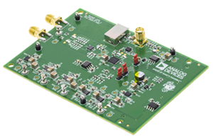
Analog Devices Inc.The?AD8400?/?AD8402?/ AD8403 provide a single, dual or quad channel, 256 position digitally controlled variable resistor (VR) device. These devices perform the same electronic adjustment function as a potentiometer or variable resistor. The AD8400 contains a single variable resistor in the compact SO-8 package. The AD8402 contains two independent variable resistors in saving SO-14 surface mount package. The AD8403 contains four independent variable resistors in 24-lead PDIP, SOIC and TSSOP packages. Each part contains a fixed resistor with a wiper contact that taps the fixed resistor value at a point determined by a digital code loaded into the controlling serial input register. The resistance between the wiper and either endpoint of the fixed resistor varies linearly with respect to the digital code transferred into the VR latch. Each variable resistor offers a completely programmable value of resistance, between the A terminal and the wiper or the B terminal and the wiper. The fixed A to B terminal resistance of 1 k?, 10 k?, 50 k? or 100 k? has a ?1% channel-to-channel matching tolerance with a nominal temperature coefficient of 500 ppm/?C. A unique switching circuit minimizes the high glitch inherent in traditional switched resistor designs avoiding any make-before-break or break-before-make operation.Each VR has its own VR latch that holds its programmed resistance value. These VR latches are updated from an SPI compatible serial-to-parallel shift register that is loaded from a standard 3-wire serial-input digital interface. Ten data bits make up the data word clocked into the serial input register. The data word is decoded where the first two bits determine the address of the VR latch to be loaded, the last eight bits are data. A serial data output pin at the opposite end of the serial register allows simple daisy-chaining in multiple VR applications without additional external decoding logic.
EVAL-AD8422ACPZ
Analog Devices Inc.The AD8422 is a high precision, low power, low noise, rail-to-rail instrumentation amplifier that delivers the best performance per unit microampere in the industry. The AD8422 processes signals with ultralow distortion performance that is load independent over its full output range.The AD8422 is the third generation development of the industry standard?AD620. The AD8422 employs new process technologies and design techniques to achieve higher dynamic range and lower errors than its predecessors, while consuming less than one-third of the power. The AD8422 uses the high performance pinout introduced by the AD8221.Very low bias current makes the AD8422 error-free with high source impedance, allowing multiple sensors to be multiplexed to the inputs. Low voltage noise and low current noise make the AD8422 an ideal choice for measuring a Wheatstone bridge.The wide input range and rail-to-rail output of the AD8422 bring all of the benefits of a high performance in-amp to single-supply applications. Whether using high or low supply voltages, the power savings make the AD8422 an excellent choice for high channel count or power sensitive applications.The AD8422 uses robust input protection that ensures reliability without sacrificing noise performance. The AD8422 has high ESD immunity, and the inputs are protected from continuous voltages up to 40 V from the opposite supply rail.A single resistor sets the gain from 1 to 1000. The reference pin can be used to apply a precise offset to the output voltage.The AD8422 is specified from ?40?C to +85?C for the 8-lead MSOP and the 8-lead SOIC_N and from ?40?C to +125?C for the 8-lead LFCSP.APPLICATIONS Medical instrumentation Industrial process controls Strain gages Transducer interfaces Precision data acquisition systems Channel-isolated systems Portable instrumentation
EVAL-AD9832SDZ
Analog Devices Inc.The AD9832 is a numerically controlled oscillator employing a phase accumulator, a sine look-up table, and a 10-bit digital-to-analog converter (DAC) integrated on a single CMOS chip. Modulation capabilities are provided for phase modulation and frequency modulation.Clock rates up to 25 MHz are supported. Frequency accuracy can be controlled to one part in 4 billion. Modulation is effected by loading registers through the serial interface.A power-down bit allows the user to power down the AD9832 when it is not in use, the power consumption being reduced to 5 mW (5 V) or 3 mW (3 V). The part is available in a 16-lead TSSOP package.Applications Frequency stimulus/waveform generation Frequency phase tuning and modulation Low power RF/communications systems Liquid and gas flow measurement Sensory applications: proximity, motion, and defect detection Test and medical equipment
EVAL-ADA4570SDZ
Analog Devices Inc.The ADA4570 is an anisotropic magnetoresistive (AMR) sensor with integrated signal conditioning amplifiers and analog-to-digital converter (ADC) drivers. The ADA4570 produces two differential analog outputs that indicate the angular position of the surrounding magnetic field. The ADA4570 consists of two die within one package, an AMR sensor, and a fixed gain instrumentation amplifier. The ADA4570 delivers amplified differential cosine and sine output signals, with respect to the angle, when the magnetic field is rotating in the x-axis and the y-axis (x-y) plane. The output voltage range is ratiometric to the supply voltage.The sensor contains two Wheatstone bridges, at a relative angle of 45? to one another. A complete rotation of a dipole magnet produces two periods on the sinusoidal outputs. Therefore, the magnetic angle (?) calculated from the SIN and COS differential outputs represents the physical orientation of the magnet with respect to the ADA4570 in the 0? to 180? measurement range. Within a homogeneous field in the x-y plane, the output signals of the ADA4570 are independent of the physical placement in the z direction (air gap).The ADA4570 is available in an 8-lead SOIC package.APPLICATIONS Absolute position measurement (linear and angle) Brushless dc motor control and positioning Actuator control and positioning Contactless angular measurement and detection Magnetic angular position sensing
EVAL-ADA4571-2EBZ
Analog Devices Inc.The ADA4571-2 is a 2-channel anisotropic magneto resistive (AMR) sensor with integrated signal conditioning amplifiersand ADC drivers. The device produces analog outputs that indicate the angular position of the surrounding magnetic field.Each channel consists of two die within one package: an AMR sensor and a variable gain instrumentation amplifier. The ADA4571-2 delivers clean and amplified cosine and sine output signals per channel related to the angle of a rotating magnetic field. The output voltage range is ratiometric to the supply voltage.Each sensing channel contains two separated wheatstone bridges at a relative angle of 45? to one another. A rotating magnetic field parallel to the plane of the IC package delivers two sinusoidal output signals, with the double frequency of the angle, ?, between the sensor and the magnetic field direction. Within a homogeneous field parallel to the plane of the IC package, the output signals are independent of airgap between the sensor and the magnet.The ADA4571-2 is available in a 16-lead SOIC package.Product Highlights Contactless angular measurement. Measures magnetic field direction rather than field intensity. Minimum sensitivity to air gap variations. Large working distance. Excellent accuracy, even for weak saturation fields. Minimal thermal and lifetime drift. Negligible hysteresis.Single-chip solution.Applications Permanent magnet synchronous motor (PMSM) control and positioning Contactless angular measurement and detection? Magnetic angular position sensing
EVAL-ADAU1467Z
Analog Devices Inc.The ADAU1463/ADAU1467 are automotive qualified audio processors that far exceed the digital signal processing capabilities of earlier SigmaDSP? devices. They are pin and register compatible with each other, as well as with theADAU1450/ADAU1451/ADAU1452 SigmaDSP? processors. The restructured hardware architecture is optimized for efficient audio processing. The audio processing algorithms support a seamless combination of stream processing (sample-by-sample), multirate processing, and block processing paradigms. The SigmaStudio? graphical programming tool enables the creation of signal processing flows that are interactive, intuitive, and powerful. The enhanced digital signal processor (DSP) core architecture enables some types of audio processing algorithms to be executed using significantly fewer instructions than were required on previous SigmaDSP generations, leading to vastly improved code efficiency.The 1.2 V, 32-bit DSP core can run at frequencies of up to 294.912 MHz and execute up to 6144 single instruction, multiple data (SIMD) instructions per sample at the standard sample rate of 48 kHz. Powerful clock generator hardware, including a flexible phase-locked loop (PLL) with multiple fractional integer outputs, supports all industry standard audio sample rates. Nonstandard rates over a wide range can generate up to 15 sample rates simultaneously. These clock generators, along with the on-board asynchronous sample rate converters (ASRCs) and a flexible hardware audio routing matrix, make the ADAU1463/ADAU1467 ideal audio hubs that greatly simplify the design of complex multirate audio systems.The ADAU1463/ADAU1467 have four input serial ports and four output serial ports. Each device has an asynchronous clock domain capable of operating as either a bit clock and frame sync master or slave. Each of the serial ports supports multiple data lines. The eight SDATAIOx pins each can be associated with any of the four input or four output serial ports. The use of assignable data pins allows a serial port to transmit or receive additional channels of audio data using a single bit clock and frame clock. Each of the supplemental data pins can carry from two to eight channels of serial audio. This flexible configuration provides more channels of audio input/output (I/O) without the need to run serial ports at high speed, and enables systems with additional serial audio peripherals. These expanded serial audio ports, along with the clock generators, the on-board asynchronous sample rate converters (ASRCs), and a flexible hardware audio routing matrix make the ADAU1463/ ADAU1467 ideal audio hubs that greatly simplify the design of complex, multirate audio systems.The ADAU1463/ADAU1467 interface with a wide range of analog-to-digital converters (ADCs), digital-to-analog converters (DACs), digital audio devices, amplifiers, and control circuitry with highly configurable serial ports, I2C, serial peripheral interface (SPI), Sony/Philips Digital Interconnect Format (S/PDIF) interfaces, and multipurpose I/O pins. Dedicated decimation filters can decode the pulse density modulation (PDM) output of up to four MEMS microphones.Independent slave and master I2C/SPI control ports allow the ADAU1463/ADAU1467 to be programmed and controlled by an external master device such as a microcontroller, and to program and control slave peripherals directly. Self boot functionality and the master control port enable complex standalone systems.Note that throughout this data sheet, multifunction pins, such as SDATAIO4/MP20, are referred to either by the entire pin name or by a single function of the pin, for example, MP20, when only that function is relevant.Applications Automotive audio processing Head units Distributed amplifiers Rear seat entertainment systems Trunk amplifiers Commercial and professional audio processing
EVAL-ADAU1772Z
Analog Devices Inc.The ADAU1772 is a codec with four inputs and two outputs that incorporates a digital processing engine to perform filtering, level control, signal level monitoring, and mixing. The path from the analog input to the DSP core to the analog output is optimized for low latency and is ideal for noise cancelling headsets. With the addition of just a few passive components, a crystal, and an EEPROM for booting, the ADAU1772 provides a complete headset solution.APPLICATIONS Noise cancelling headsets, headsets, and headphones BlueTooth ANC headsets, headsets, and headphones Personal navigation devices Digital still and video cameras
EVAL-ADAU1966AZ
Analog Devices Inc.The ADAU1966A is a high performance, single-chip digital-to-analog converter (DAC) that provides 16 DACs with differential or single-ended outputs using the Analog Devices, Inc., patented multibit sigma-delta (?-?) architecture. A serial peripheral interface (SPI)/I2C port is included, allowing a microcontroller to adjust volume and many other parameters. The ADAU1966A operates from 2.5 V digital and 3.3 V analog supplies. A linear regulator is included to generate the digital supply voltage from the analog supply voltage. The ADAU1966A is available in an 80-lead LQFP.The ADAU1966A is designed for low EMI. This consideration is apparent in both the system and circuit design architectures. By using the on-board PLL to derive the internal master clock from an external left-right frame clock (LRCLK), the ADAU1966A can eliminate the need for a separate high frequency master clock and can be used with or without a bit clock. The DACs are designed using the latest Analog Devices continuous time architectures to further minimize EMI. By using 2.5 V digital supplies, power consumption is minimized, and the digital waveforms are a smaller amplitude, further reducing emissions.Note that throughout this data sheet, multifunction pins, such as SCLK/SCL, are referred to by the entire pin name or by a single function of the pin, for example, SCLK, when only that function is relevant.APPLICATIONS Automotive audio systems Home theater systems Digital audio effects processors
EVAL-ADAU7118Z
Analog Devices Inc.The ADAU7118 converts four stereo pulse density modulation (PDM) bitstreams into one pulse code modulation (PCM) output stream. The source for the PDM data can be eight microphones or other PDM sources. The PCM audio data is output on a serial audio interface port in either inter-IC serial (I2S) or time domain multiplexed (TDM) format.The ADAU7118 is specified over the commercial temperature range (?40?C to +85?C). The ADAU7118 is available in a 16-lead, 3 mm ? 3 mm, 0.40 mm pitch, lead frame chip scale package (LFCSP).Note that throughout this data sheet, multifunction pins, such as ADDR/CONFIG, are referred to either by the entire pin name or by a single function of the pin, for example, ADDR, when only that function is relevant.Applications Microphone arrays Mobile computing Portable electronics Consumer electronics Professional electronics
EVAL-ADCM
Analog Devices Inc.The ADcmXL3021 is a complete vibration sensing system that combines high performance vibration sensing (using micro-electromechanical systems (MEMS) accelerometers) with a variety of signal processing functions to simplify the development of smart sensor nodes in condition-based monitoring (CBM) systems. The typical ultralow noise density (26 ?g/?Hz) in the MEMS accelerometers supports excellent resolution. The wide bandwidth (dc to 10 kHz within 3 dB flatness) enables tracking of key vibration signatures on many machine platforms.The signal processing includes high speed data sampling (220 kSPS), 4096 time sample record lengths, filtering, windowing, fast Fourier transform (FFT), user configurable spectral or time statistic alarms, and error flags. The serial peripheral interface (SPI) provides access to a register structure that contains the vibration data and a wide range of user configurable functions.The ADcmXL3021 is available in a 23.7 mm ? 27.0 mm ? 12.4 mm aluminum package with four mounting flanges to support installation with standard machine screws. This package provides consistent mechanical coupling to the core sensors over a broad frequency range. The electrical interface is through a 14-pin connector on a 36 mm flexible cable, which enables a wide range of location and orientation options for system mating connectors.The ADcmXL3021 requires only a single, 3.3 V power supply and supports an operating temperature range of ?40?C to +105?C.Applications Vibration analysis CBM systems Machine health Instrumentation and diagnostics Safety shutoff sensing
EVAL-ADCMP396EBZ
Analog Devices Inc.The ADCMP396 is a quad, rail-to-rail input, low power comparator ideal for use in general-purpose applications. The device operates from a supply voltage of 2.3 V to 5.5 V and draws a minimal amount of current. The quad ADCMP396 consumes only 41.6 ?A of supply current. The low voltage and low current operation of the ADCMP396 makes it ideal for battery-powered systems.The ADCMP396 features a common-mode input voltage range of 200 mV beyond rails, an offset voltage of 1 mV typical across the full common-mode range, and a UVLO monitor. In addition, the design of the comparator allows a defined output state upon power-up. The comparator generates a logic low output while the supply voltage is less than the UVLO threshold.The ADCMP396 incorporates a 1 V ? 0.9% buffered reference voltage. The reference voltage output can directly connect to the comparator input to serve as the trip value for precise monitoring and detection of positive voltage. It can also act as an offset when monitoring the negative voltage.The ADCMP396 is available in a 16-lead narrow-body SOIC package, and it is specified to operate over the ?40?C to +125?C extended temperature range.APPLICATIONS Battery management/monitoring Power supply detection Window comparator Threshold detectors/discriminators Microprocessor systems
EVAL-ADCMP581BCPZ
Analog Devices Inc.The ADCMP580/ADCMP581/ADCMP582 are ultrafast voltagecomparators fabricated on the Analog Devices, Inc. proprietaryXFCB3 Silicon Germanium (SiGe) bipolar process. TheADCMP580 features CML output drivers, the ADCMP581features reduced swing ECL (negative ECL) output drivers, andthe ADCMP582 features reduced swing PECL (positive ECL)output drivers.All three comparators offer 180 ps propagation delay and 100 psminimum pulse width for 10 Gbps operation with 200 fs randomjitter (RJ). Overdrive and slew rate dispersion are typically lessthan 15 ps.The ?5 V power supplies enable a wide ?2 V to +3 V inputrange with logic levels referenced to the CML/NECL/PECLoutputs. The inputs have 50 ? on-chip termination resistorswith the optional capability to be left open (on an individualpin basis) for applications requiring high impedance input. The CML output stage is designed to directly drive 400 mV into50 ? transmission lines terminated to ground. The NECL outputstages are designed to directly drive 400 mV into 50 ? terminatedto ?2 V. The PECL output stages are designed to directly drive400 mV into 50 ? terminated to VCCO ? 2 V. High speed latchand programmable hysteresis are also provided. The differentiallatch input controls are also 50 ? terminated to an independentVTT pin to interface to either CML or ECL or to PECL logic.The ADCMP580/ADCMP581/ADCMP582 are available in a16-lead LFCSP.Applications Automatic test equipment (ATE) High speed instrumentation Pulse spectroscopy Medical imaging and diagnostics High speed line receivers Threshold detection Peak and zero-crossing detectors High speed trigger circuitry Clock and data signal restoration
EVAL-ADCMP600BRJZ
Analog Devices Inc.The ADCMP600, ADCMP601, and ADCMP602 are very fast comparators fabricated on Analog Devices? proprietary XFCB2 process. These comparators are exceptionally versatile and easy to use. Features include an input range from ? 0.5 V to VCC + 0.2 V, low noise TTL-/CMOS-compatible output drivers, and latch inputs with adjustable hysteresis and/or shutdown inputs.The devices offer 5 ns propagation delay with 10 mV overdrive on 3 mA typical supply current.A flexible power supply scheme allows the devices to operate with a single +2.5 V positive supply and a ?0.5 V to +2.8 V input signal range up to a +5.5 V positive supply with a ?0.5 V to +5.8 V input signal range. Split input/output supplies with no sequencing restrictions on the ADCMP602 support a wide input signal range while still allowing independent output swing control and power savings.The TTL-/CMOS-compatible output stage is designed to drive up to 5 pF with full timing specs and to degrade in a graceful and linear fashion as additional capacitance is added. The comparator input stage offers robust protection against large input overdrive, and the outputs do not phase reverse when the valid input signal range is exceeded. High speed latch and programmable hysteresis features are also provided with a unique single-pin control option.The ADCMP600 is available in both 5-lead SC70 and SOT-23 packages, the ADCMP601 is available in a 6-lead SC70 package, and the ADCMP602 is available in 8-lead MSOP and LSCFP packages.Applications High Speed Instrumentation Clock and Data Signal Restoration Logic Level Shifting or Translation Pulse Spectroscopy High Speed Line Receivers Threshold Detection Peak and Zero-crossing Detectors High Speed Trigger Circuitry Pulse-width Modulators Current-/voltage-controlled Oscillators Automatic Test Equipment (ATE)
EVAL-ADCMP609BRMZ
Analog Devices Inc.The ADCMP609 is a fast comparator fabricated on XFCB2, an Analog Devices, Inc., proprietary process. These comparators are exceptionally versatile and easy to use. Features include an input range from VEE ? 0.2 V to VCC + 0.2 V, low noise, TTL-/CMOS-compatible output drivers, and adjustable hysteresis and/or shutdown inputs.The device offers 40 ns propagation delay driving a 15 pF load with 10 mV overdrive on 500 ?A typical supply current.A flexible power supply scheme allows the devices to operate with a single +2.5 V positive supply and a ?0.2 V to +3.0 V input signal range up to a +5.5 V positive supply with a ?0.2 V to +5.7 V input signal range.The TTL-/CMOS-compatible output stage is designed to drive up to 15 pF with full rated timing specifications and to degrade in a graceful and linear fashion as additional capacitance is added. The input stage of the comparator offers robust protection against large input overdrive, and the outputs do not phase reverse when the valid input signal range is exceeded. A programmable hysteresis feature is also provided.The ADCMP609, available in an 8-lead MSOP package, features a shutdown pin and hysteresis control.ApplicationsHigh speed instrumentation Clock and data signal restoration Logic level shifting or translation High speed line receivers Threshold detection Peak and zero-crossing detectors High speed trigger circuitry Pulse-width modulators Current-/voltage-controlled oscillators Data Sheet, Rev. A, 8/07
EVAL-ADE7878AEBZ
Analog Devices Inc.The ADE7854A?/?ADE7858A?/?ADE7868A?/?ADE7878A are high accuracy, 3-phase electrical energy measurement ICs with serial interfaces and three flexible pulse outputs. The devices incorporate second-order ?-? analog-to-digital converters (ADCs), a digital integrator, reference circuitry, and all signal processing required to perform total (fundamental and harmonic) active, reactive (ADE7858A, ADE7868A, and ADE7878A), and apparent energy measurement and rms calculations.The ADE7878A can also perform fundamental-only active and reactive energy measurement and rms calculations. A fixed function digital signal processor (DSP) executes the signal processing. The DSP program is stored in the internal ROM memory.The ADE7854A / ADE7858A / ADE7868A / ADE7878A can measure active, reactive, and apparent energy in various 3-phase configurations, such as wye or delta services, with both three and four wires. Aside from regular rms measurements, which are updated every 8 kHz, these devices measure low ripple rms values, which are averaged internally and updated every 1.024 sec. The devices provide system calibration features for each phase, that is, rms offset correction, phase calibration, and gain calibration.The CF1, CF2, and CF3 logic outputs provide a wide selection of power information. All four devices provide total active and apparent powers, as well as the sum of the current rms values; the ADE7858A, ADE7868A, and ADE7878A also provide total reactive powers; the ADE7878A also provides fundamental active and reactive powers.The ADE7854A / ADE7858A / ADE7868A / ADE7878A contain waveform sampling registers that allow access to all ADC outputs. The devices also incorporate power quality measurements, such as short duration low or high voltage detection, short duration high current variation, line voltage period measurement, and angles between phase voltages and currents.Two serial interfaces, serial peripheral interface (SPI) and I2C, can communicate with the devices. A dedicated high speed interface, the high speed data capture (HSDC) port, can be used in conjunction with I2C to provide access to the ADC outputs and real-time power information.The devices have two interrupt request pins, IRQ0 and IRQ1, to indicate that an enabled interrupt event has occurred. For the ADE7868A / ADE7878A, three specially designed low power modes ensure the continuity of energy accumulation when the ADE7868A / ADE7878A are in a tampering situation.
EVAL-ADE7880EBZ
Analog Devices Inc.The ADE7880 is high accuracy, 3-phase electrical energy measurement IC with serial interfaces and three flexible pulse outputs. The ADE7880 device incorporates second-order sigma-delta (?-?) analog-to-digital converters (ADCs), a digital integrator, reference circuitry, and all of the signal processing required to perform the total (fundamental and harmonic) active, and apparent energy measurements, rms calculations, as well as fundamental-only active and reactive energy measurements. In addition, the ADE7880 computes the rms of harmonics on the phase and neutral currents and on the phase voltages, together with the active, reactive, and apparent power, and the power factor and harmonic distortion on each harmonic for all phases. Total harmonic distortion plus noise (THD + N) is computed for all currents and voltages. A fixed function digital signal processor (DSP) executes this signal processing. The DSP program is stored in the internal ROM memory.The ADE7880 is suitable for measuring active, reactive, and apparent energy in various 3-phase configurations, such as wye or delta services with both three and four wires. The ADE7880 provides system calibration features for each phase, that is, rms offset correction, phase calibration, and gain calibration. The CF1, CF2, and CF3 logic outputs provide a wide choice of power information: total active powers, apparent powers, or the sum of the current rms values, and fundamental active and reactive powers.The ADE7880 contains waveform sample registers that allow access to all ADC outputs. The devices also incorporate power quality measurements, such as short duration low or high voltage detections, short duration high current variations, line voltage period measurement, and angles between phase voltages and currents. Two serial interfaces, SPI and I2C, can be used to communicate with the ADE7880. A dedicated high speed interface, the high speed data capture (HSDC) port, can be used in conjunction with I2C to provide access to the ADC outputs and real-time power information. The ADE7880 also has two interrupt request pins, IRQ0 and IRQ1, to indicate that an enabled interrupt event has occurred. Three specially designed low power modes ensure the continuity of energy accumulation when the ADE7880 is in a tampering situation. The ADE7880 is available in the 40-lead LFCSP, Pb-free package, pin-for-pin compatible with ADE7854, ADE7858, ADE7868, and ADE7878?devices.APPLICATIONS Energy metering systems Power quality monitoring Solar inverters Process monitoring Protective devices
EVAL-ADE7953EBZ
Analog Devices Inc.The ADE7953 is a high accuracy electrical energy measurementIC intended for single phase applications. It measures line voltageand current and calculates active, reactive, and apparent energy,as well as instantaneous rms voltage and current.The device incorporates three ?-? ADCs with a high accuracyenergy measurement core. The second input channel simultaneouslymeasures neutral current and enables tamper detectionand neutral current billing. The additional channel incorporatesa complete signal path that allows a full range of measurements.Each input channel supports independent and flexible gain stages,making the device suitable for use with a variety of current sensorssuch as current transformers (CTs) and low value shunt resistors.Two on-chip integrators facilitate the use of Rogowski coil sensors.The ADE7953 provides access to on-chip meter registers via avariety of communication interfaces including SPI, I2C, and UART.Two configurable low jitter pulse output pins provide outputs thatare proportional to active, reactive, or apparent energy, as well ascurrent and voltage rms. A full range of power quality informationsuch as overcurrent, overvoltage, peak, and sag detection areaccessible via the external IRQ pin. Independent active, reactive,and apparent no-load detections are included to prevent ?metercreep.? Dedicated reverse power (REVP), zero-crossing voltage(ZX), and zero-crossing current (ZX_I) pins are also provided. TheADE7953 energy metering IC operates from a 3.3 V supply voltageand is available in a 28-lead LFCSP package.
EVAL-ADF4150HVEB1Z
Analog Devices Inc.The ADF4150HV is a 3.0 GHz, fractional-N or integer-N frequency synthesizer with an integrated high voltage charge pump. The synthesizer can be used to drive external wideband VCOs directly, eliminating the need for operational amplifiers to achieve higher tuning voltages. This simplifies design and reduces cost while improving phase noise, in contrast to active filter topologies, which tend to degrade phase noise compared to passive filter topologies.The VCO frequency can be divided by 1, 2, 4, 8, or 16 to allow the user to generate RF output frequencies as low as 31.25 MHz. For applications that require isolation, the RF output stage can be muted. The mute function is both pin- and software-controllable.A simple 3-wire interface controls all on-chip registers. The charge pump operates from a power supply ranging from 6 V to 30 V, whereas the rest of the device operates from 3.0 V to 3.6 V. The ADF4150HV can be powered down when not in use.Applications Wireless infrastructure Microwave point-to-point/point-to-multipoint radios VSAT radios Test equipment Private/land mobile radio
EVAL-ADF4151EB1Z
Analog Devices Inc.The ADF4151 allows implementation of fractional-N or integer-N phase-locked loop (PLL) frequency synthesizers if used with an external voltage controlled oscillator (VCO), loop filter, and external reference frequency.The ADF4151 is used with external VCO parts and is footprint and software compatible with the ADF4350. The part consists of a low noise digital phase frequency detector (PFD), a precision charge pump, and a programmable reference divider. There is a ?-? based fractional interpolator to allow programmable fractional-N division. The INT, FRAC, and MOD registers define an overall N divider [N = (INT + (FRAC/MOD))]. The RF output phase is programmable for applications that require a particular phase relationship between the output and the reference. The ADF4151 also features cycle slip reduction circuitry, leading to faster lock times without the need for modifications to the loop filter.Control of all the on-chip registers is through a simple 3-wire interface. The device operates with a power supply ranging from 3.0 V to 3.6 V that can be powered down when not in use.The ADF4151 is available in a 5 mm ? 5 mm package.Applications Wireless infrastructure (W-CDMA, TD-SCDMA, WiMax, GSM, PCS, DCS, DECT) Test equipment Wireless LANs, CATV equipment Clock generation
EVAL-ADF4154EBZ1
Analog Devices Inc.The ADF4154 is a fractional-N frequency synthesizer that implements local oscillators in the up conversion and down conversion sections of wireless receivers and transmitters. It consists of a low noise digital phase frequency detector (PFD), a precision charge pump, and a programmable reference divider. There is a ?-? based fractional interpolator to allow programmable fractional-N division. The INT, FRAC, and MOD registersdefine an overall N divider (N = (INT + (FRAC/MOD))). In addition, the 4-bit reference counter (R counter) allows selectable REFIN frequencies at the PFD input. A complete phase-locked loop (PLL) can be implemented if the synthesizer is used with an external loop filter and a voltage controlled oscillator (VCO).A key feature of the ADF4154 is the fast-lock mode with a builtintimer. The user can program a predetermined count-down time value so that the PLL will remain in wide bandwidth mode, instead of having to control this time externally.Control of all on-chip registers is via a simple 3-wire interface. The device operates with a power supply ranging from 2.7 V to 3.3 V, and can be powered down when not in use.


