
LTM4605EV Demo Board | 4.5V to 20VIN, 12VOUT @ 5A
Analog Devices Inc.Demonstration circuit DC1198B-A features the LTM4605EV, the high efficiency, high density switch mode buck-boost μModule® regulator. The LTM4605EV can regulate its output voltage from an input voltage above, below, or equal to the output. The input voltage range of DC1198B-A is from 4.5V to 20V with a preset output voltage of 12V. The rated load current is 5A, although derating is necessary for certain VIN, VOUT, and thermal conditions. The switching frequency may be synchronized to an external clock from 200kHz to 400kHz. This PLL can be used not only to reduce undesirable frequency harmonics but also to parallel LTM4605 to provide high output current.

LTM4607EV Demob Board | 6-36VIN to 12V, 5A High Efficiency Buck-Boost DC/DC µModule Regulator
Analog Devices Inc.Demonstration circuit DC1198B-B features the LTM4607EV, a high efficiency, high density switch mode buck-boost power module. The LTM4607EV can regulate its output voltage from input voltage both above and below the output. The board accepts an input voltage from 6V to 36V and is set for an output voltage of 12V. The rated load current is 5A in boost mode and 12A in step-down operation. Derating is necessary for certain VIN, VOUT and thermal conditions. The switching frequency can be synchronized to external clock operating from 200kHz to 400kHz. This clock input can be used to reduce undesirable frequency harmonics and reduce input and output ripple when paralleling LTM4607 modules for even higher output current.

LT3592EDDB Demo Board | 500mA Wide Input Voltage Range Step-Down LED Driver with 10:1 Dimming
Analog Devices Inc.DC1205A: Demo Board for LT3592 500mA Wide Input Voltage Range Step-Down LED Driver with 10:1 Dimming.

LT3504 Demo Board | Quad Buck, 5.4V ≤ VIN ≤ 40V, VOUT1 - VOUT4 = 5V/3.3V/2.5V/1.8V at 1A Each
Analog Devices Inc.The demo circuit 1207A is a quad current mode PWM stepdown DC/DC converter featuring the LT3504. The demo circuit is designed for 5V, 3.3V, 2.5V and 1.8V outputs from a 5.4V to 40V input. The current capability of each channel is up to 1A. Individual soft-start and current limit for each output as well as synchronous function simplify the complex design of quad-output power converters.
Each converter is synchronized to either a common external clock input or a resistor programmable 250kHz to 2.2MHz internal oscillator. Programmable frequency allows optimization between efficiency and external component size. Each output can be independently disabled using its own RUN/SS pin.

LTC3605EUF Demo Board | 4V ≤ VIN ≤ 15V, VOUT = 2.5V/3.3V/5V @ 5A
Analog Devices Inc.Demonstration circuit 1215 is a step-down converter, using the LTC3605 monolithic synchronous buck regulator. The DC1215A has a maximum input voltage 15V, and is capable of delivering up to 5A of output current at a minimum input voltage of 4V. The output voltage of the DC1215A can be set as low as 0.6V, the reference voltage of the LTC3605.

DC1217A
Analog Devices Inc.The LTC3230 is a low noise charge pump DC/DC converter designed to drive 4 Main LEDs and 1 Sub LED, plus two 200mA linear regulators to provide additional system power. The LTC3230 charge pump requires only four small ceramic capacitors and one current set resistor to form a complete LED power supply and current controller.Built-in soft-start circuitry prevents excessive inrush cur- rent during start-up and mode changes. High switching frequency enables the use of small external capacitors. Main and Sub full-scale current settings are programmed by a single external resistor. Charge pump efficiency is optimized based on the voltage across the LED current sources. The part powers up in 1x mode and automatically switches to the next higher mode, 1.5x and subsequently 2x, whenever any LED current source approaches dropout.Two 200mA linear regulators have independent enable and output voltage select pins. Each regulator can be set to one of three pre-selected output voltages with tri-level input pins. The regulators may be enabled independently of the charge pump.The LTC3230 is available in a low profile (0.75mm) 3mm x 3mm 20-lead QFN package.Applications Multi-LED Driver and Dual LDO Supplies for Cell Phone, PDA, Digital Camera and PND Applications?

LTC3537EUD | 600mA (I sw) Synchronous Boost Converter and 100mA LDO in 3mmmm x 3mm QFN
Analog Devices Inc.DC1242A: Demo Board for the LTC3537 - 2.2 MHz, 600mA Synchronous Step-Up DC/DC Converter and 100mA LDO

LTC3890EGN-1 Demo Board | 4.5V ≤ VIN ≤ 60V, VOUT1 = 3.3V @ 5A, VOUT2 = 8.5V @ 3A
Analog Devices Inc.Demonstration circuit 1244 is a Low Quiescent Current, Dual Output Synchronous Buck Converter featuring the LTC3890EGN-1. DC1244 converts a 4.5V to 60V voltage source to 3.3V at 5.0A and 8.5V at 3.0A. When the input voltage is close to or below 9V, the 8.5V output enters dropout mode.The "-1" version has a fixed current limit and current foldback. See data sheet for other differences.

LT3582EUD Demo Board | 2.7V-5.5VIN, Programmable Vout Boost and Inverting DC/DC Converters with OTP (Requires DC590)
Analog Devices Inc.Demonstration circuit 1247A features the LT3582 an I2C Programmable Boost and Single Inductor Inverting DC/DC Converters with OTP. It converts a 2.7V-5.5V source to two outputs, a positive and a negative. The positive output can be programmed from 3.2V to 12.775V at 25mV intervals and the negative from -1.2V to -13.95V at 50mV intervals, all via the QuickEval™ System. A DC590B is needed for evaluation of this demo board. Table 1 below shows the maximum expected load currents for some output/input combinations. Check Maximum Load Current section on datasheet for other combinations. The LT3582 features all integrated switches and feedback resistors, a low noise control scheme, positive output disconnect function, low quiescent current, built in softstart.

LTC4012CUF-2 Demo Board | Multi-Chemistry, 3A Sync Buck Battery Charger with PowerPath Control
Analog Devices Inc.Demonstration circuit DC1256A is a single-battery standalone battery charger that can support any version ofthe LTC4012 family of parts. The LTC4012 family of charge controller IC’s do not support charge termination for any specific battery chemistry. Any charger termination, if necessary, is accomplished outside the LTC4012 with the most common method using a microcontroller. The DC1256A is shipped with the LTC4012-2 installed,which is optimized for Li-ion charge applications using a 4.2V/cell float voltage.The charger output voltage is programmed by jumpers to support 1, 2, 3 and 4 series stack Li-ion batteries. The input voltage is can be between 6V and 20V with the maximum voltage of the Demo Board design limited by the input capacitor voltage ratings. To reach full charge,the minimum input voltage must be greater than the float voltage setting.

LTC6410-6 4-Port Demo Board
Analog Devices Inc.DC1264A: Demo Board for the LTC6410-6 Low Distortion, Low Noise Differential IF Amplifier with Configurable Input Impedance

LTC3862EGN-1 Demo Board | 8V to 36VIN, 48VOUT @ 5A, Multiphase Boost Controller
Analog Devices Inc.Demonstration circuit 1286A is DC/DC boost converter featuring the LTC3862EGN/-1 constant frequency current mode boost controllers. The DC1286A-A (LTC3862) operates over 5V to 36V input and provides 2A-5A of output current at 48V output. The DC1286A-B (LTC3862-1, higher VIN min and higher gate drive) operates over 8V to 36V input and provides 3A-5A of output current at 48V output. The 200kHz constant frequency operation results in small and efficient circuit. The converter provides high output voltage accuracy (typically ±3%) over wide load range with no minimum load requirement. The demonstration circuit can be easily modified to generate different output voltages.

LTC3775EUD Demo Board | 5V ≤ VIN ≤ 26V, VOUT = 1.2V @ 15A
Analog Devices Inc.Demonstration circuit 1290A is a high frequency synchronous step-down converter featuring the LTC3775EUD. The package style for the LTC3775EUD is a 16-pin 3mm x 3mm QFN. Two versions of the demonstration board are available. DC-1290A-A has been optimized for 5V to 26V input and typically provides 1.2V/15A, while the DC1290A-B is optimized for 5V to 36VIN range and typically provides 1.2V/10A.

LTC3556EUFD Demo Board | High Efficiency USB Power Manager with Dual Buck-Buck Boost DC/DC
Analog Devices Inc.DC1296A: Demo Board for the LTC3556 High Efficiency USB Power Manager with Dual Buck and Buck-Boost DC/DCs

LTC3725EMSE/LTC3726EGN 1/4 Brick | 9V < VIN < 36V, VOUT: 12V/8.4A
Analog Devices Inc.DC1300A-B: Demo Board for:
LTC3725 - Single-Switch Forward Controller and Gate Driver
LTC3726 - Secondary-Side Synchronous Forward Controller

LT1952EGN-1/LTC3900 Demo Board | Active Reset, VIN=9V-36V VOUT=12V @ 5A
Analog Devices Inc.Demonstration circuit 1317A-G is an isolated input to high current output 1/8th brick footprint synchronous forward converter featuring the LT1952 switching controller with Active Reset circuit. The Active Reset circuit can improve the efficiency in wide input voltage applications. Also, the Active Reset allows the implementation of self-driven synchronous secondary rectifiers in some applications. The DC1317A-G converts an isolated 9V to 36V input to 12V at 5A of output current.

DC1323A
Analog Devices Inc.The LT3686 is a current mode PWM step-down DC/DC converter with an internal 1.2A power switch, packaged in 10-lead 3mm ? 3mm DFN. The wide input range of 3.6V to 37V makes the LT3686 suitable for regulating power from a wide variety of sources, including 24V industrial supplies and automotive batteries. Its high maximum frequency allows the use of tiny inductors and capacitors, resulting in a very small solution. Operating frequency above the AM band avoids interfering with radio reception, making the LT3686 particularly suitable for automotive applications.Cycle-by-cycle current limit and DA current sense provide protection against fault conditions. Soft-start and frequency foldback eliminate input current surge during start-up. An optional internal regulated active load at the output via the BD pin keeps the LT3686 at full switching frequency at light loads, resulting in low, predictable output ripple above the audio and AM bands. Internal compensation and an internal boost diode reduce external component count. Overvoltage Protections Features LT3686 55V - LT3686A 60V External Synchronization Applications Automotive Systems Battery-Powered Equipment Wall Transformer Regulation Distributed Supply Regulation

LT3599EFE Demo Board | 4-Channel Boost LED Driver, 8V ≤ PVIN ≤ 16V, VLED up to 44V @ 80mA
Analog Devices Inc.Demonstration circuit 1327B is a 4-Channel 80mA LED Driver with +/-1.5% Current Matching featuring the LT3599. The LT3599 is a step-up DC/DC converter designed to drive up to 4-strings of LEDs at up to 120mA per string, and with an output voltage up to 44V. The LED strings are connected to internal current sources where the current level is set with an external resistor. Each string can have up to 10 white LEDs. Paralleling of strings is allowed.
The LT3599 runs from a 3.1V to 5.5V power supply, and the step-up converter is powered from an 8V to 16 voltage supply, though higher voltages up to 40V may be acceptable depending on the circuit requirements.
DC1329A
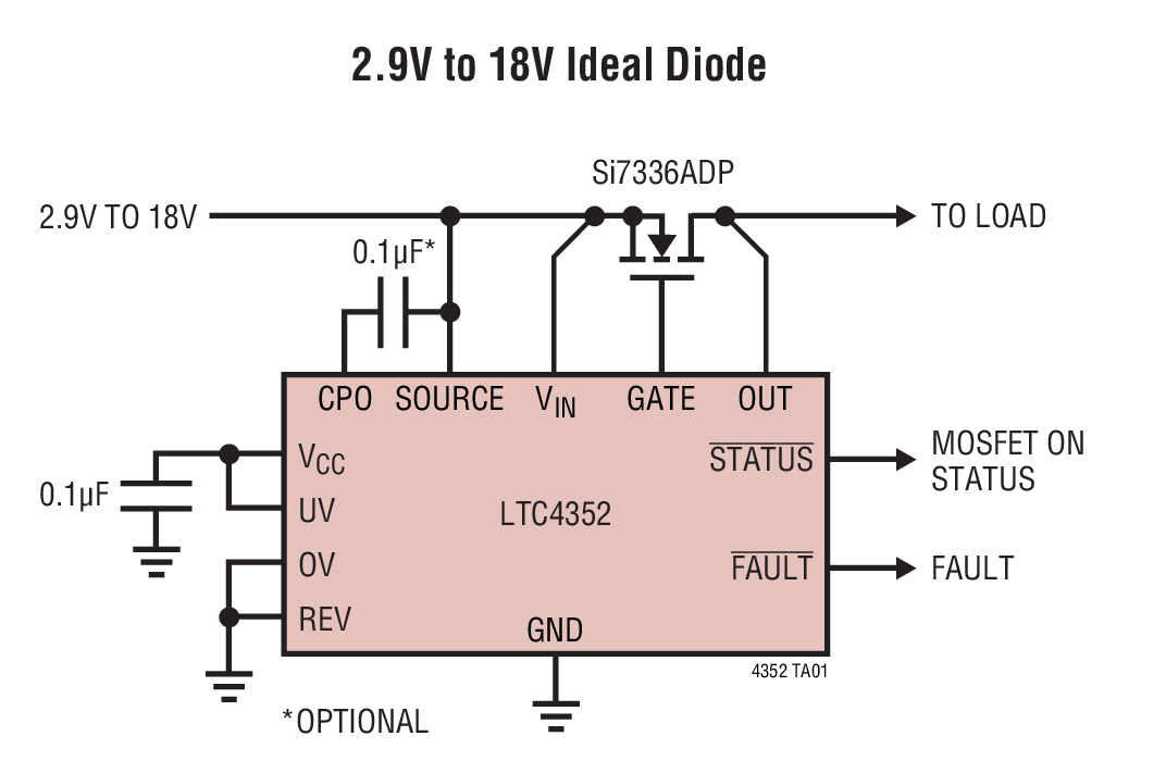
Analog Devices Inc.The LTC4352 creates a near-ideal diode using an external N-channel MOSFET. It replaces a high power Schottky diode and the associated heat sink, saving power and board area. The ideal diode function permits low loss power ORing and supply holdup applications. The LTC4352 regulates the forward voltage drop across the MOSFET to ensure smooth current transfer in diode-OR applications. A fast turn-on reduces the load voltage droop during supply switch-over. If the input supply fails or is shorted, a fast turn-off minimizes reverse currents. The controller operates with supplies from 2.9V to 18V. For lower voltages, an external supply is needed at the VCC pin. Power passage is disabled during undervoltage or overvoltage conditions. The controller also features an open MOSFET detect circuit that ?ags excessive voltage drop across the pass transistor in the on state. A REV pin enables reverse current, overriding the diode behavior when desired.Applications Redundant Power Supplies Supply Holdup Telecom Infrastructure Computer Systems and Servers

DC1332B-A
Analog Devices Inc.The LTC2631 is a family of 12-, 10-, and 8-bit voltage-output DACs with an integrated, high accuracy, low-drift reference in an 8-lead TSOT-23 package. It has a rail-to-rail output buffer that is guaranteed monotonic.The LTC2631-L has a full-scale output of 2.5V, and operates from a single 2.7V to 5.5V supply. The LTC2631-H has a full-scale output of 4.096V, and operates from a 4.5V to 5.5V supply. A 10ppm/?C reference output is available at the REF pin.Each DAC can also operate in External Reference mode, in which a voltage supplied to the REF pin sets the fullscale output.The LTC2631 DACs use a 2-wire, I2C-compatible serial interface. The LTC2631 operates in both the standard mode (clock rate of 100kHz) and the fast mode (clock rate of 400kHz).The LTC2631 incorporates a power-on reset circuit. Options are available for reset to zero-scale or reset to mid-scale after power-up.Applications Mobile Communications Process Control and Industrial Automation Automatic Test Equipment Portable Equipment Automotive Optical Networking


