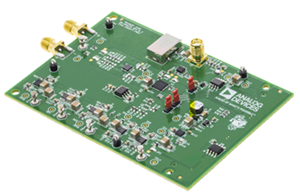
AD9762-EBZ
Analog Devices Inc.The AD9762 is the 12-bit resolution member of the TxDAC series of high performance, low power CMOS digital-to-analog converters (DACs). The TxDAC family which consists of pin compatible 8-, 10-, 12-, and 14-bit DACs is specifically optimized for the transmit signal path of communication systems. All of the devices share the same interface options, small outline package and pinout, thus providing an upward or downward component selection path based on performance, resolution and cost. The AD9762 offers exceptional ac and dc performance while supporting update rates up to 125 MSPS.The AD9762's flexible single-supply operating range of 2.7 V to 5.5 V and low power dissipation are well suited for portable and low power applications. Its power dissipation can be further reduced to a mere 45 mW without a significant degradation in performance by lowering the full-scale current output. Also, a powerdown mode reduces the standby power dissipation to approximately 25 mW.The AD9762 is manufactured on an advanced CMOS process. A segmented current source architecture is combined with a proprietary switching technique to reduce spurious components and enhance dynamic performance. Edge-triggered input latches and a 1.2 V temperature compensated bandgap reference have been integrated to provide a complete monolithic DAC solution. Flexible supply options support +3 V and +5 V CMOS logic families.The AD9762 is a current-output DAC with a nominal full-scale output current of 20 mA and > 100 k(ohm) output impedance.Differential current outputs are provided to support single-ended or differential applications. Matching between the two current outputs ensures enhanced dynamic performance in a differential output configuration. The current outputs may tied directly to an output resistor to provide two complementary, single-ended voltage outputs or fed directly into a transformer. The output voltage compliance range is 1.25 V.The on-chip reference and control amplifier are configured for maximum accuracy and flexibility. The AD9762 can be driven by the on-chip reference or by a variety of external reference voltages. The internal control amplifier which provides a wide (>10:1) adjustment span allows the AD9762 full-scale current to be adjusted over a 2 mA to 20 mA range while maintaining excellent dynamic performance. Thus, the AD9762 may operate at reduced power levels or be adjusted over a 20 dB range to provide additional gain ranging capabilities.The AD9762 is available in a 28-pin SOIC package. It is specified for operation over the industrial temperature range.
AD9789-EBZ
Analog Devices Inc.The AD9789 is a flexible QAM encoder/interpolator/upconverter combined with a high performance, 2400 MSPS, 14-bit RF digital-to-analog converter (DAC). The flexible digital interface can accept up to four channels of complex data. The QAM encoder supports constellation sizes of 16, 32, 64, 128, and 256 with SRRC filter coefficients for all standards.The on-chip rate converter supports a wide range of baud rates with a fixed DAC clock. The digital upconverter can place the channels from 0 to 0.5 ? fDAC. This permits four contiguous channels to be synthesized and placed anywhere from dc to fDAC.The AD9789 includes a serial peripheral interface (SPI) for device configuration and status register readback. The flexible digital interface can be configured for data bus widths of 4, 8, 16, and 32 bits. It can accept real or complex data.The AD9789 operates from 1.5 V, 1.8 V, and 3.3 V supplies for a total power consumption of 1.6 W. It is supplied in a 164-ball chip scale package ball grid array for lower thermal impedance and reduced package parasitics. No special power sequencing is required. The clock receiver powers up muted to prevent start-up noise.Product Highlights Highly integrated and configurable QAM mappers, interpolators, and upconverters for direct synthesis of one to four DOCSIS- or DVB-C-compatible channels in a block. Low noise and intermodulation distortion (IMD) performance enable high quality synthesis of signals up to 1 GHz. Flexible data interface supports LVDS for improved SFDR or CMOS input data for less demanding applications. Interface is configurable from 4-bit nibbles to 32-bit words and can run at up to 150 MHz CMOS or 150 MHz LVDS double data rate (DDR). Manufactured on a CMOS process, the AD9789 uses a proprietary switching technique that enhances dynamic performance.Applications Broadband communications systems CMTS/DVB Cellular infrastructure Point-to-point wireless
AD9910/PCBZ
Analog Devices Inc.The AD9910 is a direct digital synthesizer (DDS) featuringan integrated 14-bit DAC and supporting sample rates up to1 GSPS. The AD9910 employs an advanced, proprietary DDStechnology that provides a significant reduction in power consumptionwithout sacrificing performance. The DDS/DACcombination forms a digitally programmable, high frequency,analog output synthesizer capable of generating a frequencyagile sinusoidal waveform at frequencies up to 400 MHz.The user has access to the three signal control parameters thatcontrol the DDS: frequency, phase, and amplitude. The DDSprovides fast frequency hopping and frequency tuning resolutionwith its 32-bit accumulator. With a 1 GSPS sample rate, thetuning resolution is ~0.23 Hz. The DDS also enables fast phaseand amplitude switching capability.The AD9910 is controlled by programming its internal controlregisters via a serial I/O port. The AD9910 includes an integratedstatic RAM to support various combinations of frequency, phase,and/or amplitude modulation. The AD9910 also supports a userdefined, digitally controlled, digital ramp mode of operation. Inthis mode, the frequency, phase, or amplitude can be variedlinearly over time. For more advanced modulation functions, ahigh speed parallel data input port is included to enable directfrequency, phase, amplitude, or polar modulation.The AD9910 is specified to operate over the extended industrialtemperature range.Applications Agile local oscillator (LO) frequency synthesis Programmable clock generators FM chirp source for radar and scanning systems Test and measurement equipment Acousto-optic device drivers Polar modulators Fast frequency hopping
AD9912A/PCBZ
Analog Devices Inc.The AD9912 is a direct digital synthesizer (DDS) that features an integrated 14-bit digital-to-analog converter (DAC). The AD9912 features a 48-bit frequency tuning word (FTW) that can synthesize frequencies in step sizes no larger than 4 ?Hz. Absolute frequency accuracy can be achieved by adjusting the DAC system clock.The AD9912 also features an integrated system clock phase-locked loop (PLL) that allows for system clock inputs as low as 25 MHz.The AD9912 operates over an industrial temperature range, spanning ?40?C to +85?C.APPLICATIONS Agile LO frequency synthesis Low jitter, fine tune clock generation Test and measurement equipment Wireless base stations and controllers Secure communications Fast frequency hopping
AD9988-FMCB-EBZ
Analog Devices Inc.The AD9988 is a highly integrated device with four 16-bit, 12 GSPS maximum sample rate, RF digital-to-analog converter (DAC) cores, and four 12-bit, 4 GSPS rate, RF analog-to-digital converter (ADC) cores. The device supports four transmitter channels and four receiver channels with a 4T4R configuration. This product is well suited for four-antenna TDD transmitter applications, where the receiver path can be shared between receiver and observation modes. The GPIO pins can be configured and toggled to support different user modes, while phase coherency is maintained. The maximum radio channel bandwidth supported is 1.2 GHz in a 4T4R configuration and a sample resolution of 16 bits. The AD9988 features a 16-lane 24.75 Gbps JESD204C or 15.5 Gbps JESD204B serial data port that allows up to eight lanes per transmit/receive link, an on-chip clock multiplier, and digital signal processing capability targeted at multiband direct to RF radio applications.APPLICATIONSWireless communications infrastructureW-CDMA, LTE, LTE-A, massive multiple input multiple output (MIMO)Point to point microwave, E-band, and 5G mmWaveBroadband communications systemsDOCSIS 3.0+ cable modem termination system (CMTS)Communication test and measurement systems
ADA4807-4ARUZ-EBZ
Analog Devices Inc.The ADA4807-1 (single), ADA4807-2 (dual), and ADA4807-4 (quad) are low noise, rail-to-rail input and output, voltage feedback amplifiers. These amplifiers combine low power, low noise, high speed, and dc precision to provide an attractive solution for a wide range of applications from high resolution data acquisition instrumentation to high performance battery-powered and high component density systems where power consumption is of key importance.With only 1.0 mA of supply current per amplifier, the ADA4807-1/ADA4807-2/ADA4807-4 feature the lowest input voltage noise?among high speed, rail-to-rail input/output amplifiers in the industry and offer a wide bandwidth, high slew rate, fast settling time, and excellent distortion performance. Additionally, these amplifiers offer very low input offset voltage and drift performance, making them ideal for driving multiplexed and high throughput?precision 16-/18-bit successive approximation registers (SARs) and 24-bit ?-? ADCs.These amplifiers are fully specified at +3 V, +5 V, and ?5 V supplies and can operate over the industrial ?40?C to +125?C?temperature range.The ADA4807-1 is available in 6-lead SOT-23 and space-saving 6-lead SC70 packages. The ADA4807-2 is available in an 8-lead?MSOP and a compact, 3 mm ? 3 mm, 10-lead LFCSP. The ADA4807-4 is available in a 14-lead TSSOP package.Applications High resolution analog-to-digital converter (ADC) drivers Portable and battery-powered instruments and systems? High component density data acquisition systems Audio signal conditioning Active filters
ADA4850-2YCP-EBZ
Analog Devices Inc.The ADA4850-1/ADA4850-2 are low price, high speed, voltagefeedbacks rail-to-rail output op amps with ultralow power-down.Despite their low price, the ADA4850-1/ADA4850-2 provideexcellent overall performance and versatility. The 175 MHz,?3 dB bandwidth and 220 V/?s slew rate make these amplifierswell-suited for many general-purpose, high speed applications.The ADA4850-1/ADA4850-2 are designed to operate at supplyvoltages as low as 2.7 V and up to 6 V at 2.4 mA of supplycurrent per amplifier. In power-down mode, the supply currentis less than 150 nA, ideal for battery-powered applications.The ADA4850-1/ADA4850-2 family provides users with a truesingle-supply capability, allowing input signals to extend200 mV below the negative rail and to within 2.2 V of thepositive rail. The output of the amplifier can swing within80 mV of either supply rail.With its combination of low price, excellent differential gain(0.12%), differential phase (0.09?), and 0.1 dB flatness out to14 MHz, these amplifiers are ideal for video applications. The ADA4850-1/ADA4850-2 are designed to work in theextended temperature range of ?40?C to +125?C. Applications Portable multimedia players Video cameras Digital still cameras Consumer video Clock buffers
ADA4853-3YCP-EBZ
Analog Devices Inc.The ADA4853-1/ADA4853-2/ADA4853-3 are low power, low cost, high speed, rail-to-rail output op amps with ultralow power disables that are ideal for portable consumer electronics. Despite their low price, the ADA4853-1/ADA4853-2/ADA4853-3 provide excellent overall performance and versatility. The 100 MHz, ?3 dB bandwidth, and 120 V/?s slew rate make these amplifiers well-suited for many general-purpose, high speed applications.The ADA4853-1/ADA4853-2/ADA4853-3 voltage feedback op amps are designed to operate at supply voltages as low as 2.65 V and up to 5 V using only 1.4 mA of supply current per amplifier. To further reduce power consumption, the amplifiers are equipped with a power-down mode that lowers the supply current to less than 1.5 ?A maximum, making them ideal in battery-powered applications.The ADA4853-1/ADA4853-2/ADA4853-3 provide users with a true single-supply capability, allowing input signals to extend 200 mV below the negative rail and to within 1.2 V of the positive rail. On the output, the amplifiers can swing within 200 mV of either supply rail.With their combination of low price, excellent differential gain (0.2%), differential phase (0.10?), and 0.5 dB flatness out to 22 MHz, these amplifiers are ideal for video applications.The ADA4853-1 is available in a 6-lead SC70, the ADA4853-2 is available in a 16-lead LFCSP_WQ, and the ADA4853-3 is available in both a 16-lead LFCSP_WQ and a 14-lead TSSOP. The ADA4853-1 temperature range is ?40?C to +85?C while the ADA4853-2/ADA4853-3 temperature range is ?40?C to +105?C.Applications Automotive infotainment systems Automotive safety systems Portable multimedia players Video cameras Digital still cameras Consumer video Clock buffer
ADA4853-3YRU-EBZ
Analog Devices Inc.The ADA4853-1/ADA4853-2/ADA4853-3 are low power, low cost, high speed, rail-to-rail output op amps with ultralow power disables that are ideal for portable consumer electronics. Despite their low price, the ADA4853-1/ADA4853-2/ADA4853-3 provide excellent overall performance and versatility. The 100 MHz, ?3 dB bandwidth, and 120 V/?s slew rate make these amplifiers well-suited for many general-purpose, high speed applications.The ADA4853-1/ADA4853-2/ADA4853-3 voltage feedback op amps are designed to operate at supply voltages as low as 2.65 V and up to 5 V using only 1.4 mA of supply current per amplifier. To further reduce power consumption, the amplifiers are equipped with a power-down mode that lowers the supply current to less than 1.5 ?A maximum, making them ideal in battery-powered applications.The ADA4853-1/ADA4853-2/ADA4853-3 provide users with a true single-supply capability, allowing input signals to extend 200 mV below the negative rail and to within 1.2 V of the positive rail. On the output, the amplifiers can swing within 200 mV of either supply rail.With their combination of low price, excellent differential gain (0.2%), differential phase (0.10?), and 0.5 dB flatness out to 22 MHz, these amplifiers are ideal for video applications.The ADA4853-1 is available in a 6-lead SC70, the ADA4853-2 is available in a 16-lead LFCSP_WQ, and the ADA4853-3 is available in both a 16-lead LFCSP_WQ and a 14-lead TSSOP. The ADA4853-1 temperature range is ?40?C to +85?C while the ADA4853-2/ADA4853-3 temperature range is ?40?C to +105?C.Applications Automotive infotainment systems Automotive safety systems Portable multimedia players Video cameras Digital still cameras Consumer video Clock buffer
ADA4855-3YCP-EBZ
Analog Devices Inc.The ADA4855-3 (triple) is a single-supply, rail-to-rail output operational amplifier. It provides excellent high speed performance with 410 MHz, ?3 dB bandwidth and a slew rate of 870 V/?s. It has a wide input common-mode voltage range that extends from 0.2 V below ground to 1 V below the positive rail.In addition, the output voltage swings within 100 mV of either supply rail, making this rail-to-rail operational amplifier easy to use on single-supply voltages as low as 3.3 V. The ADA4855-3 offers a typical low power of 7.8 mA per amplifier and is capable of delivering up to 57 mA of load current. It also features a power-down function for power sensitive applications that reduces the supply current down to 1 mA. The ADA4855-3 is available in a 16-lead LFCSP and is designed to work over the extended industrial temperature range of ?40?C to +105?C.ApplicationsProfessional videoConsumer videoImagingInstrumentationBase stationsActive filters Data Sheet, Rev. 0, 11/2008
ADA4891-4ARU-EBZ
Analog Devices Inc.The ADA4891-1 (single), ADA4891-2 (dual), ADA4891-3 (triple), and ADA4891-4 (quad) are CMOS, high speed amplifiers that offer high performance at a low cost. The amplifiers feature true single-supply capability, with an input voltage range that extends 300 mV below the negative rail. In spite of their low cost, the ADA4891 family provides high performance and versatility. The rail-to-rail output stage enables the output to swing within 50 mV of each rail, enabling maximum dynamic range. The ADA4891 family of amplifiers is ideal for imaging applications, such as consumer video, CCD buffers, and contact image sensor buffers. Low distortion and fast settling time also make them ideal for active filter applications. The ADA4891-1/ADA4891-2/ADA4891-3/ADA4891-4 are available in a wide variety of packages. The ADA4891-1 is available in 8-lead SOIC and 5-lead SOT-23 packages. The ADA4891-2 is available in 8-lead SOIC and 8-lead MSOP packages. The ADA4891-3 and ADA4891-4 are available in 14-lead SOIC and 14-lead TSSOP packages. The amplifiers are specified to operate over the extended temperature range of ?40?C to +125?C.Applications Imaging Consumer video Active filters Coaxial cable drivers Clock buffers Photodiode preamp Contact image sensor and buffers
ADA4922-1ACP-EBZ
Analog Devices Inc.The ADA4922-1 is a differential driver for 16-bit to 18-bitanalog-to-digital converters (ADCs) that have differential inputranges up to ?20 V. Configured as an easy-to-use, single-ended-to-differentialamplifier, the ADA4922-1 requires no externalcomponents to drive ADCs. The ADA4922-1 provides essentialbenefits such as low distortion and high SNR that are requiredfor driving ADCs with resolutions up to 18 bits.With a wide supply voltage range (5 V to 26 V), high inputimpedance, and fixed differential gain of 2, the ADA4922-1 isdesigned to drive ADCs found to in a variety of applications,including industrial instrumentation. The ADA4922-1 is manufactured on Analog Devices, Inc.,proprietary, second-generation XFCB process that enables theamplifier to achieve excellent noise and distortion performanceon high supply voltages.The ADA4922-1 is available in an 8-lead 3 mm ? 3 mm LFCSPas well as an 8-lead SOIC package. Both packages are equippedwith an exposed paddle for more efficient heat transfer. TheADA4922-1 is rated to work over the extended industrialtemperature range, ?40?C to +85?C. Applications High voltage data acquisition systems Industrial instrumentation Spectrum analysis ATE Medical instruments
ADA4945-1CP-EBZ
Analog Devices Inc.The ADA4945-1 is a low noise, low distortion, fully differential amplifier with two selectable power modes. The device operates over a broad power supply range of 3 V to 10 V. The low dc offset, dc offset drift, and excellent dynamic performance of the ADA4945-1 makes it well suited for a variety of data acquisition and signal processing applications. The device is an ideal choice for driving high resolution, high performance successive approximation register (SAR) and ?-? analog-to-digital converters (ADCs) on 4 mA of quiescent current (full power mode). The device can also be selected to operate on 1.4 mA of quiescent current (low power mode) to scale the power consumption to the desired performance necessary for an ADC drive application. The adjustable common-mode voltage allows the ADA4945-1 to match the input common-mode voltage of multiple ADCs. The internal common-mode feedback loop provides exceptional output balance, as well as suppression of even order harmonic distortion products.With the ADA4945-1, differential gain configurations are achieved with a simple external feedback network of four resistors determining the closed-loop gain of the amplifier. The ADA4945-1 is fabricated using Analog Devices, Inc., proprietary, silicon germanium (SiGe), complementary bipolar process, enabling the device to achieve low levels of distortion with an input voltage noise of only 1.8 nV/?Hz (full power mode).The ADA4945-1 is available in a RoHS-complaint, 3 mm ? 3 mm, 16-lead LFCSP. The ADA4945-1 is specified to operate from ?40?C to +125?C.Applications Low power ?-?, PulSAR?, and SAR ADC drivers Single-ended to differential converters Differential buffers Medical imaging Process control Portable electronics
ADCA5190-EVALZ
Analog Devices Inc.The ADCA5190 is a medium power gain block amplifier that provides excellent linearity across a flexible bias range allowing power efficient design implementation for various applications. The device provides 19.1 dB of flat gain up to 1800 MHz, making this ideal for Data Over Cable Service Interface Specification (DOCSIS?) 4.0 downstream applications. The device is also well suited for upstream applications to 700 MHz as the output stage. The device is conveniently packaged in an industry-standard, 32-lead, 5 mm ? 5 mm lead frame chip-scale package (LFCSP) with an exposed pad on the bottom of the package for improved thermal performance.APPLICATIONS 45 MHz to 1800 MHz CATV infrastructure amplifier systems 5 MHz to 700 MHz upstream Remote physical layer (PHY) DOCSIS 3.1 and DOCSIS 4.0 compliant
ADCA5191-EVALZ
Analog Devices Inc.The ADCA5191 is a medium power gain block amplifier that provides excellent linearity across a flexible bias range allowing power efficient design implementation for various applications.The device provides 25.8 dB of flat gain up to 1800 MHz, making this ideal for Data Over Cable Service Interface Specification (DOCSIS) 4.0 downstream applications. The device is also well suited for upstream applications to 700 MHz as the output stage. It is conveniently packaged in an industry-standard, 5 mm ? 5 mm, 32-lead, lead frame chip-scale package (LFCSP) with an exposed pad on the bottom of the package for improved thermal performance.APPLICATIONS45 MHz to 1800 MHz CATV infrastructure amplifier systems5 MHz to 700 MHz upstreamRemote physical layer (PHY)DOCSIS? 3.1 and DOCSIS 4.0 compliant
ADCLK905/PCBZ
Analog Devices Inc.The ADCLK905 (one input, one output), ADCLK907 (dual oneinput, one output), and ADCLK925 (one input, two outputs) areultrafast clock/data buffers fabricated on the Analog Devices, Inc.,proprietary XFCB3 silicon germanium (SiGe) bipolar process.The ADCLK905/ADCLK907/ADCLK925 feature full-swing emitter coupled logic (ECL) output drivers. For PECL (positive ECL) operation, bias VCC to the positive supply and VEE to ground. For NECL (negative ECL) operation, bias VCC to ground and VEE to the negative supply.The buffers offer 95 ps propagation delay, 7.5 GHz toggle rate, 10 Gbps data rate, and 60 fs random jitter (RJ).The inputs have center tapped, 100 ?, on-chip termination resistors. A VREF pin is available for biasing ac-coupled inputs.The ECL output stages are designed to directly drive 800 mV each side into 50 ? terminated to VCC ? 2 V for a total differential output swing of 1.6 V.The ADCLK905/ADCLK907/ADCLK925 are available in 16-lead LFCSP packages.Applications Clock and data signal restoration and level shifting Automated test equipment (ATE) High speed instrumentation High speed line receivers Threshold detection Converter clocking
ADD5211CP-EVALZ
Analog Devices Inc.The ADD5211 is a four-string, white LED driver for backlight applications based on high efficiency, current mode, step-up converter technology. The boost controller drives an external MOSFET switch for step-up regulation from an input voltage of 4.5 V to 40 V and a pin adjustable operating frequency from 200 kHz to 1.2 MHz. An adjustable UVLO function is implemented to reduce input current during power-off.The ADD5211 provides four regulated current sinks for uniform brightness intensity. Each current sink can be driven from 40 mA to 200 mA; the LED driving current is pin adjustable using an external resistor. With an input PWM interface, the ADD5211 drives up to four parallel strings of multiple series connected LEDs.Additional features include LED short protection, LED open protection, boost output short protection, overvoltage protection, cycle-by-cycle current limit, and thermal shutdown for both the IC and the LED array. An open-drain fault output is also included. A programmable soft start is implemented to reduce inrush current during startup. Applications LCD monitor and TV LED backlights Industrial lighting
ADF70301-169EZKIT
Analog Devices Inc.The ADF7030-1 is a fully integrated, radio transceiver achieving high performance at very low power. The ADF7030-1 is ideally suited for applications that require long range, network robustness, and long battery life. It is suitable for applications that operate in the ISM, SRD, and licensed frequency bands at 169.4 MHz to 169.6 MHz, 426 MHz to 470 MHz, and 863 MHz to 960 MHz. It provides extensive support for standards-based protocols like IEEE802.15.4g while also providing flexibility to support a wide range of proprietary protocols.The highly configurable low intermediate frequency (IF) receiver supports a large range of receiver channel bandwidths from 2.6 kHz to 406 kHz. This range of receiver channel bandwidths allows the ADF7030-1 to support ultranarrow-band, narrow-band, and wideband channel spacing.The ADF7030-1 features two independent PAs supporting output power ranges of ?20 dBm to +13 dBm and ?20 dBm to +17 dBm. The PAs support ultrafine adjustment of the power with a step resolution of 0.1 dB. The PA output power is exceptionally robust over temperature and voltage. The PAs have an automatic power ramp control to limit spectral splatter to meet regulatory standards.The ADF7030-1 features an on-chip ARM??Cortex?-M0 processor that performs radio control, radio calibration, and packet management. Cortex-M0 eases the processing burden of the host processor because the ADF7030-1 integrates the lower layers of a typical communication protocol stack. This internal processor also permits the download and execution of Analog Devices, Inc., provided firmware modules that can extend the functionality of the ADF7030-1.The ADF7030-1 has two packet modes: generic packet mode and IEEE802.15.4g mode. In generic packet mode, the packet format is highly flexible and fully programmable, thereby ensuring its compatibility with proprietary packet formats. In IEEE802.15.4g packet mode, the packet format conforms to the?IEEE802.15.4g standard. FEC, as per the IEEE802.15.4g standard, is also supported.The ADF7030-1 operates with a power supply range of 2.2 V to 3.6 V and has very low power consumption in both Tx and Rx modes, enabling long lifetimes in battery-operated systems. An ultralow power deep sleep mode achieves a typical current of 10 nA with the configuration memory retained.A complete wireless solution can be built using a small number of external discrete components and a host processor (typically a microcontroller). The host processor can configure the ADF7030-1 using a simple command-based protocol over a standard 4-wire SPI interface. A single-byte command transitions the radio between states or performs a radio function.The ADF7030-1 is available in two package types: a 6 mm ? 6 mm, 40-lead LFCSP and a 7 mm ? 7 mm, 48-lead LQFP. Both package types use NiPdAu plating to mitigate against silver migration in high humidity applications. The ADF7030-1 operating temperature range is ?40?C to +85?C.For Figure 13 to Figure 19, Figure 30, Figure 42, Figure 60, Figure 61, and Figure 75 in the Typical Performance Characteristics section, PA_COARSE is a programmable value that provides a coarse adjustment of the PA output power. This value can be programmed in the range of 1 to 6 for PA1, and from 1 to 10 for PA2. PA_FINE is a programmable value that provides a fine adjustment of the PA output power. This value can be programmed in the range of 3 to 127 for both PA1 and PA2. PA_MICRO is a programmable value that provides a microadjustment (typically
ADIS16507-1/PCBZ
Analog Devices Inc.The ADIS16507 is a precision, miniature microelectromechanical?system (MEMS) inertial measurement unit (IMU) that includes?a triaxial gyroscope and a triaxial accelerometer. Each inertial?sensor in the ADIS16507 combines with signal conditioning?that optimizes dynamic performance. The factory calibration?characterizes each sensor for sensitivity, bias, alignment,?linear acceleration (gyroscope bias), and point of percussion?(accelerometer location). As a result, each sensor has dynamic?compensation formulas that provide accurate sensor?measurements over a broad set of conditions.The ADIS16507 provides a simplified, cost effective method for?integrating accurate, multiaxis inertial sensing into industrial?systems, especially when compared with the complexity and?investment associated with discrete designs. All necessary motion?testing and calibration are part of the production process at the?factory, greatly reducing system integration time. Tight orthogonal?alignment simplifies inertial frame alignment in navigation?systems. The serial peripheral interface (SPI) and register?structure provide a simple interface for data collection and?configuration control.The ADIS16507 is available in a 100-ball, ball grid array (BGA)?package that is approximately 15 mm ? 15 mm ? 5 mm.Applications Navigation, stabilization, and instrumentation Unmanned and autonomous vehicles Smart agriculture and construction machinery Factory/industrial automation, robotics Virtual/augmented reality Internet of Moving Things


