
117201-HMC631LP3
Analog Devices Inc.The HMC631LP3 & HMC631LP3E are high dynamic range Vector Modulator RFICs which are targeted for RF predistortion and feed-forward cancellation circuits, as well as RF cancellation, beam forming and amplitude/phase correction circuits. The I & Q ports of the HMC631LP3(E) can be used to continuously vary the phase and amplitude of RF signals by up to 360 degrees and 40 dB respectively, while supporting a 3 dB modulation bandwidth of 200 MHz. With an output IP3 of +26 dBm and output noise floor of -160 dBm/Hz (at maximum gain setting), the IP3/noise floor ratio is 186 dB.APPLICATIONS Cellular/3G & WiMAX Systems Wireless Infrastructure HPA & MCPA Error Correction Pre-Distortion or Feed-Forward Linearization Beam Forming & Nulling Circuits

117212-HMC624ALP4
Analog Devices Inc.The HMC624A is a 6-bit digital attenuator with a 31.5 dB attenuation control range in 0.5 dB steps.The HMC624A offers excellent attenuation accuracy and high input linearity over the specified frequency range from 100 MHz to 6.0 GHz. However, this digital attenuator features external ac grounding capacitors to extend the operation below 100 MHz.The HMC624A is integrated with two dies: a CMOS driver and a gallium arsenide (GaAs) RF attenuator. The CMOS driver provides both serial and parallel control of the RF attenuator. The device also features a user-selectable power-up state and a serial output port for cascading other serial controlled components.The HMC624A operates with a single positive supply voltage from 3 V to 5 V, and provides a CMOS-/TTL-compatible control interface.The HMC624A comes in a RoHS compliant, compact, 4 mm ? 4 mm LFCSP package, and is pin compatible to the HMC1122 except for the ACGx pins.Applications Cellular infrastructure Microwave radios and very small aperture terminals (VSATs) Test equipment and sensors Intermediate frequency (IF) and radio frequency (RF) designs?

118100-HMC646LP2
Analog Devices Inc.The HMC646LP2(E) is an SPDT switch in a leadless DFN surface mount plastic package for use in transmit / receive and LNA protection applications which require very low distortion and high power handling of up to 40 watts with less than 10% duty cycle. This robust switch can control signals from 100 - 2100 MHz* and is ideal for TD-SCDMA / 3G repeaters, PMR, automotive telematics, and satellite subscriber terminal applications. The design provides exceptional P0.1 dB of +46 dBm and +74 dBm IIP3 on the Transmit (Tx) port. The failsafe topology provides a low loss path from Tx to RFC, when no DC power is available.APPLICATIONS LNA Protection & T/R Switching TD-SCDMA / 3G Infrastructure Satellite Subscriber Terminals Private Mobile Radio & Public Safety Handsets Automotive Telematics

121493-HMC611LP4
Analog Devices Inc.The HMC611LP4(E) Logarithmic Detector/Controller converts RF signals at its input, to a proportional DC voltage at its output. The HMC611LP4(E) employs a successive compression topology which delivers extremely high dynamic range and conversion accuracy over a wide input frequency range. As the input power is increased, successive amplifiers move into saturation one by one creating an accurate approximation of the logarithm function.The output of a series of square law detectors is summed, converted into voltage domain and buffered to drive the LOGOUT output. For detection mode, the LOGOUT pin is shorted to the VSET input, and will provide a nominal logarithmic slope of -25mV/dB and an intercept of 18 dBm (22 dBm for ? ? 5.8 GHz). The HMC611LP4(E) can also be used in the controller mode where an external voltage is applied to the VSET pin, to create an AGC or APC feedback loop.Applications Cellular/PCS/3G WiMAX, WiBro, WLAN, Fixed Wireless & Radar Power Monitoring & Control Circuitry Receiver Signal Strength Indication (RSSI) Automatic Gain & Power Control
121561-HMC700LP4
Analog Devices Inc.The HMC700LP4(E) is a SiGe BiCMOS fractional-N frequency synthesizer. The synthesizer includes a very low noise digital phase frequency detector (PFD), and a precision controlled charge pump.The fractional synthesizer features an advanced deltasigma modulator design that allows both ultra-fine step sizes and very low spurious products. Spurious outputs are low enough to eliminate the need for costly Direct Digital Synthesis (DDS) references in many applications.The HMC700LP4(E) phase-frequency detector (PFD) features cycle slip prevention (CSP) technology that allows faster frequency hopping times.Ultra low in-close phase noise and low spurious also permit architectures with wider loop bandwidths for faster frequency hopping and low micro-phonics. FSK mode allows the synthesizer to be used as a simple low cost direct FM transmitter source.Applications Base Stations for Mobile Radio WiMAX Test & Measurement CATV Equipment Phased Array Applications Simple FSK Links DDS Replacement

122410-HMC686LP4E
Analog Devices Inc.The HMC686LP4(E) is a high dynamic range passive MMIC mixer with integrated LO amplifier in a 4x4 SMT QFN package covering 0.7 to 1.1 GHz. Excellent input IP3 performance of +34 dBm for down conversion is provided for 3G & 4G GSM/CDMA applications at an LO drive of 0 dBm. With an input 1 dB compression of +25 dBm, the RF port will accept a wide range of input signal levels. Conversion loss is 7.5 dB typical. The DC to 500 MHz IF frequency response will satisfy GSM/CDMA transmit or receive frequency plans.The HMC686LP4(E) is optimized to high side LO frequency plans for 0.7 - 1.1 GHz RF Band and is pin for pin compatible with the?HMC684LP4(E)?which is a 0.7 - 1.0 GHz converter optimized for low side LO. The HMC686LP4(E) is optimized to low side LO frequency plans for 1.4 - 1.5 GHz RF LTE band applications.APPLICATIONS Cellular/3G & LTE/WiMAX/4G Basestations & Repeaters GSM, CDMA & OFDM Transmitters and Receivers

122789-HMC504LC4B
Analog Devices Inc.The HMC504LC4B is a GaAs MMIC Low NoiseWideband Amplifier housed in a leadless 4?4 mm ceramicsurface mount package. The amplifier operatesbetween 14 and 27 GHz, providing up to 19 dB ofsmall signal gain, 2.2 dB noise figure, and output IP3of +26 dBm, while requiring only 90 mA from a +4Vsupply. The P1dB output power of up to +17 dBmenables the LNA to function as a LO driver for balanced,I/Q or image reject mixers. The HMC504LC4Balso features I/Os that are DC blocked and internallymatched to 50 ?, making it ideal for high capacitymicrowave radios or VSAT applications. This versatileLNA is also available in die form as the HMC-ALH476.APPLICATIONSThis HMC504LC4B is ideal for: Point-to-Point Radios Point-to-Multi-Point Radios Military & Space Test Instrumentation

122826-HMC753LP4E
Analog Devices Inc.The HMC753 is a GaAs MMIC Low Noise Wideband Amplifier housed in a leadless 4x4 mm plastic surface mount package. The amplifier operates between 1 and 11 GHz, providing up to 16.5 dB of small signal gain, 1.5 dB noise figure, and output IP3 of +30 dBm, while requiring only 55 mA from a +5V supply. The P1dB output power of up to +18 dBm enables the LNA to function as a LO driver for balanced, I/Q or image reject mixers. The HMC753 also features I/Os that are DC blocked and internally matched to 50 Ohms, making it ideal for high capacity microwave radios or VSAT applications. This versatile LNA is also available in die form as the?HMC-ALH444.Applications Point-to-Point Radios Point-to-Multi-Point Radios Military & Space Test Instrumentation.

123585-HMC859LC3
Analog Devices Inc.The HMC859LC3 is a Divide-by-8 with Reset designed to support clock frequencies as high as 26 GHz. During normal operation, with the reset pin not asserted, the output toggles from its prior state on the positive edge of the clock. Asserting the reset pin forces the Q output low regardless of the clock edge state (asynchronous reset assertion). Reversing the clock inputs allows for negative-edge triggered applications. The HMC859LC3 also features an output level control pin, VR, which allows for loss compensation or for signal level optimization.All input signals to the HMC859LC3 are terminated with 50 ? to ground on-chip, and may be either AC or DC coupled. Outputs can be connected directly to a 50 ? terminated system, while DC blocking capacitors may be used if the terminating system is 50 ? to a non-ground DC voltage. The HMC859LC3 operates from a single -3.3 V DC supply and is available in a ceramic RoHS compliant 3x3 mm SMT package.APPLICATIONS High Speed Frequency Divider?(up to 26 GHz) Clock Synthesis Phase Locked Loops Broadband Test & Measurement

124022-HMC799LP3E
Analog Devices Inc.The HMC799LP3E is DC to 700 MHz Transimpedance amplifier designed for opto-electronic laser sensor applications, FDDI receivers and receiver systems employing optical to electrical conversion. This amplifier provides a single-ended output voltage that is proportional to an applied current at its input port. This current is typically provided by a photodiode. Operating from a single +5V supply, HMC799LP3E features very low input referred noise, and very large electrical input dynamic range exceeding 65 dB. 10 kOhm or 80 dB-Ohms transimpedance gain provides very good sensitivity at higher data rates.The output of HMC799LP3E is internally matched to 50 ohms. External matching is not necessary. The HMC799LP3E exhibits excellent gain and output power stability over temperature, while requiring a minimal number of external bias components.Applications Laser Sensor FDDI Receiver CATV FM Analog Receiver Wideband Gain Block Low Noise RF Applications
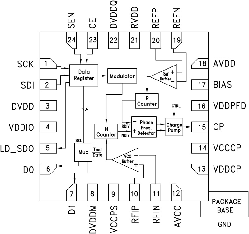
124111-HMC700LP4
Analog Devices Inc.The HMC700LP4(E) is a SiGe BiCMOS fractional-N frequency synthesizer. The synthesizer includes a very low noise digital phase frequency detector (PFD), and a precision controlled charge pump.The fractional synthesizer features an advanced deltasigma modulator design that allows both ultra-fine step sizes and very low spurious products. Spurious outputs are low enough to eliminate the need for costly Direct Digital Synthesis (DDS) references in many applications.The HMC700LP4(E) phase-frequency detector (PFD) features cycle slip prevention (CSP) technology that allows faster frequency hopping times.Ultra low in-close phase noise and low spurious also permit architectures with wider loop bandwidths for faster frequency hopping and low micro-phonics. FSK mode allows the synthesizer to be used as a simple low cost direct FM transmitter source.Applications Base Stations for Mobile Radio WiMAX Test & Measurement CATV Equipment Phased Array Applications Simple FSK Links DDS Replacement

124390-HMC741ST89E
Analog Devices Inc.The HMC741 is an InGaP Heterojunction Bipolar Transistor (HBT) Gain Block MMIC SMT amplifier covering 0.05 to 3 GHz. Packaged in an industry standard SOT89, the amplifier can be used as a cascadable 50 Ohm RF or IF gain stage as well as a PA or LO driver with up to +18.5 dBm output power. The HMC741 offers 20 dB of gain with a +42 dBm output IP3 at 200 MHz, and can operate directly from a +5V supply. The HMC741 exhibits excellent gain and output power stability over temperature, while requiring a minimal number of external bias components.Applications Cellular/3G & WiMAX/4G Fixed Wireless & WLAN CATV, Cable Modem & DBS Microwave Radio & Test Equipment IF & RF Applications

124842-HMC794LP3E
Analog Devices Inc.The HMC794LP3E is a SiGe BiCMOS low noise programmable frequency divider in a 3 ? 3mm leadless surface mount package. The circuit can be programmed to divide from N = 1 to N = 4 in the 200 MHz to 2 GHz input frequency range. The high level output power (up to 10 dBm) with a very low SSB phase noise and 50% duty cycle makes this device ideal for low noise clock generation, LO generation and LO drive applications. Configurable bias controls allow power minimization of up to 20%.APPLICATIONS LO Generation with Low Noise Floor Clock Generators Mixer LO Drive Military Applications Test Equipment Sensors

125604-HMC701LP6CE
Analog Devices Inc.The HMC701LP6CE is a SiGe BiCMOS fractional-N frequency synthesizer. The synthesizer includes a 8GHz 16-bit RF N-Divider, a 24-bit delta-sigma modulator, a very low noise digital phase frequency detector (PFD), and a precision controlled charge pump. In addition the synthesizer supports an external step tuned VCO.The fractional synthesizer features an advanced delta-sigma modulator design that allows ultra-fine frequency step sizes. The synthesizer features the ability to alter both the phase-frequency detector (PFD) gain and the cycle slipping characteristics of the PFD. This feature can reduce the time to arrive at the new frequency by 50% vs. conventional PFDs. Ultra low in-close phase noise also allows wider loop bandwidths for faster frequency hopping.The synthesizer contains a built-in linear sweeper function, which allows it to perform frequency chirps with a wide variety of sweep times, polarities and dwells, all with an external or automatic sweep trigger.A General Purpose Output (GPO) bus supports the use of multiple VCOs. In addition the synthesizer has a number of auxiliary clock generation modes that can be accessed via the GPO.Applications Base Stations for Mobile Radio (GSM, PCS, DCS, CDMA, WCDMA) Wireless LANs, WiMax Communications Test Equipment CATV Equipment FMCW Sensors Automotive Radar Phased-Array Systems

125614-HMC851LC3C
Analog Devices Inc.The HMC851LC3C is a XOR/XNOR gate function designed to support data transmission rates of up to 28 Gbps, and clock frequencies as high as 28 GHz. The HMC851LC3C also features an output level control pin, VR, which allows for loss compensation or for signal level optimization.All input signals to the HMC851LC3C are terminated with 50 Ohms to ground on-chip, and may be either AC or DC coupled. The differential outputs of the HMC851LC3C may be either AC or DC coupled. Outputs can be connected directly to a 50 Ohm to ground terminated system, while DC blocking capacitors may be used if the terminating system is 50 Ohms to a nonground DC voltage. The HMC851LC3C operates from a single -3.3V DC supply, and is available in a ceramic RoHS compliant 3x3 mm SMT package.APPLICATIONS RF ATE Applications Broadband Test & Measurement Serial Data Transmission?up to 28 Gbps

125682-HMC789ST89E
Analog Devices Inc.The HMC789ST89E is a high linearity GaAs InGaP HBT gain block MMIC operating from 0.7 to 2.8 GHz and packaged in an industry standard SOT89 package. Utilizing a minimum number of external components and a single +5V supply, the amplifier output IP3 can be optimized to +45 dBm. The high output IP3 and high gain make the HMC789ST89E ideal for use in PA driver & pre-driver applications in Cellular/4G and Fixed Wireless.Applications Cellular/4G Fixed Wireless & WLAN CATV, Cable Modem & DBS Microwave Radio & Test Equipment IF & RF Applications
126222-HMC789ST89E
Analog Devices Inc.The HMC789ST89E is a high linearity GaAs InGaP HBT gain block MMIC operating from 0.7 to 2.8 GHz and packaged in an industry standard SOT89 package. Utilizing a minimum number of external components and a single +5V supply, the amplifier output IP3 can be optimized to +45 dBm. The high output IP3 and high gain make the HMC789ST89E ideal for use in PA driver & pre-driver applications in Cellular/4G and Fixed Wireless.Applications Cellular/4G Fixed Wireless & WLAN CATV, Cable Modem & DBS Microwave Radio & Test Equipment IF & RF Applications

126578-HMC855LC5
Analog Devices Inc.The HMC855LC5 is a 1:4 demultiplexer designed for data deserialization up to 28 Gbps. The device uses both rising and falling edges of the half-rate clock to sample the input data in sequence, D0-D3 and latches the data onto the differential outputs. A quarter-rate clock output generated on chip can be used to clock the data into other devices. The demux is DC coupled supporting broadband operation.All clock and data inputs to the HMC855LC5 are CML and terminated on-chip with 50 Ohms to the positive supply, GND, and may be DC or AC coupled. The differential outputs are source terminated to 50 Ohms and may also be AC or DC coupled. Outputs can be connected directly to a 50 Ohm ground terminated system, or drive devices with CML logic input. The HMC855LC5 also features an output level control pin, VR, which allows for loss compensation or signal level optimization. The HMC855LC5 operates from a single -3.3V supply and is available in RoHS compliant 5x5 mm SMT package.APPLICATIONS SONET OC-192 Broadband Test & Measurement Serial Data Transmission?up to 28 Gbps FPGA Interfacing

126968-HMC857LC5
Analog Devices Inc.The HMC857LC5 is a 2?2 Crosspoint Switch designed to support data transmission rates of up to 14 Gbps and selector port operation up to 14 GHz. The selector routes the differential inputs to either one or both of the desired outputs upon assertion of the appropriately selected port. The HMC857LC5 also features an output level control pin, VR, which allows for loss compensation or for signal level optimization.All single-ended input signals to the HMC857LC5 are terminated with 50 Ohms to ground on-chip, and may be either AC or DC coupled. The outputs of the HMC857LC5 may be operated either differentially or single ended. Outputs can be connected directly to a 50 ??terminated system, while DC blocking capacitors may be used if the terminating system is 50 Ohms to a non-ground DC voltage. The HMC857LC5 operates from a single -3.3V DC supply and is available in a ceramic RoHS compliant 5 נ5 mm SMT package.APPLICATIONS SONET OC-192 and 10 GbE 16G Fiber Channel Network & Storage Dual 2:1 Selector 1:2 Fanout with Input Mux

127102-HMC856LC5
Analog Devices Inc.The HMC856 is a wideband time delay device with a 5-bitdigital control designed for timing compensation or clock skewmanagement applications. The time delay provides nearly100 ps (maximum) of delay range with 3 ps resolution andsupports 28 Gbps data. The monotonic delay is compensatedfor stable operation over both power supply and temperaturevariation.All differential inputs to the HMC856 are current mode logic(CML) and terminated on chip with 50 ? to the positive supplyground, GND, and can be ac or dc-coupled. The differential CMLoutputs are source terminated to 50 ? and can also be ac or dccoupled.Connect outputs directly to a 50 ? ground terminatedsystem or drive devices with CML logic input. The control lines,B4 to B0, are differential CML inputs terminated with 600 ? tothe positive rail, which supports lower power control options.The HMC856 features an output level control pin, VR, thatallows loss compensation or signal level optimization. TheHMC856 operates from a single ?3.3 V supply and is availablein a 5 mm ? 5 mm LCC package. APPLICATIONS SONET OC-192 High speed serial logic Clock and data recovery Broadband test and measurement equipment Frequency synthesis Matched timing


