
AD9520-5/PCBZ
Analog Devices Inc.The AD9520-5 provides a multioutput clock distributionfunction with subpicosecond jitter performance, along withan on-chip PLL that can be used with an external VCO.The AD9520-5 serial interface supports both SPI and I2C ports.An in-package EEPROM, which can be programmed through theserial interface, can store user-defined register settings forpower-up and chip reset.The AD9520-5 features 12 LVPECL outputs in four groups. Anyof the 1.6 GHz LVPECL outputs can be reconfigured as two250 MHz CMOS outputs. If an application requires LVDSdrivers instead of LVPECL drivers, refer to the AD9522-5.Each group of three outputs has a divider that allows both thedivide ratio (from 1 to 32) and the phase offset or coarse timedelay to be set.The AD9520-5 is available in a 64-lead LFCSP and can be operatedfrom a single 3.3 V supply. The external VCO can have anoperating voltage of up to 5.5 V. A separate output driver powersupply can be from 2.375 V to 3.465 V.The AD9520-5 is specified for operation over the standardindustrial range of ?40?C to +85?C. Applications Low jitter, low phase noise clock distribution Clock generation and translation for SONET, 10Ge, 10GFC, Synchronous Ethernet, OTU2/3/4 Forward error correction (G.710) Clocking high speed ADCs, DACs, DDSs, DDCs, DUCs, MxFEs High performance wireless transceivers ATE and high performance instrumentation Broadband infrastructures

AD9522-0/PCBZ
Analog Devices Inc.The AD9522-01 provides a multioutput clock distribution function with subpicosecond jitter performance, along with an on-chip PLL and VCO. The on-chip VCO tunes from 2.53 GHz to 2.95 GHz. An external 3.3 V/5 V VCO/VCXO of up to 2.4 GHz can also be used.The AD9522 serial interface supports both SPI and I2C? ports. An in-package EEPROM can be programmed through the serial interface and store user-defined register settings for power-up and chip reset.The AD9522 features 12 LVDS outputs in four groups. Any of the 800 MHz LVDS outputs can be reconfigured as two 250 MHz CMOS outputs.Each group of outputs has a divider that allows both the divide ratio (from 1 to 32) and the phase (coarse delay) to be set.The AD9522 is available in a 64-lead LFCSP and can be operated from a single 3.3 V supply. The external VCO can have an operating voltage up to 5.5 V.The AD9522 is specified for operation over the standard industrial range of ?40?C to +85?C.The AD9520-0 is an equivalent part to the AD9522-0 featuring LVPECL/CMOS drivers instead of LVDS/CMOS drivers.ApplicationsLow jitter, low phase noise clock distributionClock generation and translation for SONET, 10Ge, 10G FC, and other 10 Gbps protocolsForward error correction (G.710)Clocking high speed ADCs, DACs, DDSs, DDCs, DUCs, MxFEsHigh performance wireless transceiversATE and high performance instrumentationBroadband infrastructures1The AD9522 is used throughout this data sheet to refer to all the members of the AD9522 family. However, when AD9522-0 is used, it is referring to that specificmember of the AD9522 family.Data Sheet, Rev. 0, 10/08

AD9525/PCBZ-VCO
Analog Devices Inc.The AD9525 is designed to support converter clock requirements for long-term evolution (LTE) and multicarrier GSM base station designs.The AD9525 provides a low power, multioutput, clock distribution function with low jitter performance, along with an on-chip PLL that can be used with an external VCO or VCXO. The VCO input and eight LVPECL outputs can operate up to a frequency of 3.6 GHz. All outputs share a common divider that can provide a division of 1 to 6.The AD9525 offers a dedicated output that can be used to provide a programmable signal for resetting or synchronizing a data converter. The output signal is activated by a SPI write.The AD9525 is available in a 48-lead LFCSP and can be operated from a single 3.3 V supply. The external VCXO or VCO can have an operating voltage of up to 5.5 V.The AD9525 operates over the extended industrial temperature range of ?40?C to +85?C.Applications LTE and multicarrier GSM base stations Clocking high speed ADCs, DACs ATE and high performance instrumentation 40/100Gb/s OTN Line Side Clocking Cable/DOCSIS CMTS Clocking Test and Measurement

AD9528/PCBZ
Analog Devices Inc.The AD9528 is a two-stage PLL with an integrated JESD204B SYSREF generator for multiple device synchronization. The first stage phase-locked loop (PLL) (PLL1) provides input reference conditioning by reducing the jitter present on a system clock. The second stage PLL (PLL2) provides high frequency clocks that achieve low integrated jitter as well as low broadband noise from the clock output drivers. The external VCXO provides the low noise reference required by PLL2 to achieve the restrictive phase noise and jitter requirements necessary to achieve acceptable performance. The on-chip VCO tunes from 3.450 GHz to 4.025 GHz. The integrated SYSREF generator outputs single shot, N-shot, or continuous signals synchronous to the PLL1 and PLL2 outputs to time align multiple devices.The AD9528 generates six outputs (Output 0 to Output 3, Output 12, and Output 13) with a maximum frequency of 1.25 GHz, and eight outputs with a maximum frequency of up to 1 GHz. Each output can be configured to output directly from PLL1, PLL2, or the internal SYSREF generator. Each of the 14 output channels contains a divider with coarse digital phase adjustment and an analog fine phase delay block that allows complete flexibility in timing alignment across all 14 outputs. The AD9528 can also be used as a dual input flexible buffer to distribute 14 device clock and/or SYSREF signals. At power-up, the AD9528 sends the VCXO signal directly to Output 12 and Output 13 to serve as the power-up ready clocks.Note that, throughout this data sheet, the dual function pin names are referenced by the relevant function where applicable.Applications High performance wireless transceivers LTE and multicarrier GSM base stations Wireless and broadband infrastructure Medical instrumentation Clocking high speed ADCs, DACs, DDSs, DDCs, DUCs, MxFEs; supports JESD204B Low jitter, low phase noise clock distribution ATE and high performance instrumentation

AD9547/PCBZ
Analog Devices Inc.The AD9547 provides synchronization for many systems, including synchronous optical networks (SONET/SDH). The AD9547 generates an output clock that is synchronized to one of two differential or four single-ended external input references. The digital PLL allows for reduction of input time jitter or phase noise associated with the external references. The AD9547 con-tinuously generates a clean (low jitter), valid output clock, even when all references fail, by means of digitally controlled loop and holdover circuitry.The AD9547 operates over an industrial temperature range of ?40?C to +85?C.ApplicationsNetwork synchronizationCleanup of reference clock jitterSONET/SDH clocks up to OC-192, including FECStratum 2 holdover, jitter cleanup, and phase transient controlStratum 3E and Stratum 3 reference clocksWireless base stations, controllersCable infrastructureData communications

AD9554-1/PCBZ
Analog Devices Inc.The AD9554-1 is a low loop bandwidth clock translator that provides jitter cleanup and synchronization for many systems,including synchronous optical networks (SONET/SDH). The AD9554-1 generates an output clock synchronized to up to four external input references. The digital PLLs (DPLLs) allowreduction of input time jitter or phase noise associated with the external references. The digitally controlled loop and holdovercircuitry of the AD9554-1 continuously generates a low jitteroutput clock even when all reference inputs have failed.The AD9554-1 operates over an industrial temperature range of ?40?C to +85?C. The AD9554 is a version of this device with two outputs per PLL. If a single or dual DPLL version of thisdevice is needed, refer to the AD9557 or AD9559, respectively.Applications Network synchronization, including synchronous Ethernet and synchronous digital hierarchy (SDH) to optical transport network (OTN) mapping/demapping Cleanup of reference clock jitter SONET/SDH clocks up to OC-192, including FEC Stratum 3 holdover, jitter cleanup, and phase transient control Cable infrastructure? Data communications? Professional video

AD9557/PCBZ
Analog Devices Inc.The AD9557 is a low loop bandwidth clock multiplier that provides jitter cleanup and synchronization for many systems, including synchronous optical networks (OTN/SONET/SDH). The AD9557 generates an output clock synchronized to up to four external input references. The digital PLL allows for reduction of input time jitter or phase noise associated with the external references. The digitally controlled loop and holdover circuitry of the AD9557 continuously generates a low jitter output clock even when all reference inputs have failed.The AD9557 operates over an industrial temperature range of ?40?C to +85?C. If more inputs/outputs are needed, refer to the AD9558 for the four-input/six-output version of the samedevice.Applications Network synchronization, including synchronous Ethernet and SDH to OTN mapping/demapping Cleanup of reference clock jitter SONET/SDH/OTN clocks up to 100 Gbps, including FEC Stratum 3 holdover, jitter cleanup, and phase transient control Wireless base station controllers Cable infrastructure Data communications

AD9575-EVALZ-PEC
Analog Devices Inc.The AD9575 provides a highly integrated, dual output clockgenerator function including an on-chip PLL core that isoptimized for network clocking. The integer-N PLL design isbased on the Analog Devices, Inc., proven portfolio of high performance, low jitter frequency synthesizers to maximize linecard performance. Other applications with demanding phasenoise and jitter requirements also benefit from this part.The PLL section consists of a low noise phase frequency detector (PFD), a precision charge pump, a low phase noise voltagecontrolled oscillator (VCO), and pin selectable feedback and output dividers.By connecting an external crystal, popular network output frequencies can be locked to the input reference. The output divider and feedback divider ratios are pin programmable for therequired output rates. No external loop filter components are required, thus conserving valuable design time and board space.The AD9575 is available in a 16-lead, 4.4 mm ? 5.0 mm TSSOP and can be operated from a single 3.3 V supply. The temperature range is ?40?C to +85?C. APPLICATIONS GbE/FC/SONET line cards, switches, and routers CPU/PCI-E applications Low jitter, low phase noise clock generation

AD9609-40EBZ
Analog Devices Inc.The AD9609 is a monolithic, single channel 1.8 V supply, 10-bit,20/40/65/80 MSPS analog-to-digital converter (ADC). It featuresa high performance sample-and-hold circuit and on-chip voltagereference.The product uses multistage differential pipeline architecturewith output error correction logic to provide 10-bit accuracy at80 MSPS data rates and to guarantee no missing codes over thefull operating temperature range.The ADC contains several features designed to maximize flexibilityand minimize system cost, such as programmable clock and dataalignment and programmable digital test pattern generation. Theavailable digital test patterns include built-in deterministic andpseudorandom patterns, along with custom user-defined testpatterns entered via the serial port interface (SPI).A differential clock input with selectable internal 1 to 8 divide ratiocontrols all internal conversion cycles. An optional duty cyclestabilizer (DCS) compensates for wide variations in the clock dutycycle while maintaining excellent overall ADC performance.The digital output data is presented in offset binary, gray code, ortwos complement format. A data output clock (DCO) is providedto ensure proper latch timing with receiving logic. Both 1.8 V and3.3 V CMOS levels are supported.The AD9609 is available in a 32-lead RoHS-compliant LFCSPand is specified over the industrial temperature range (?40?Cto +85?C).APPLICATIONS Communications Diversity radio systems Multimode digital receivers GSM, EDGE, W-CDMA, LTE, CDMA2000, WiMAX, TD-SCDMA Smart antenna systems Battery-powered instruments Handheld scope meters Portable medical imaging Ultrasound Radar/LIDAR PET/SPECT imagingPRODUCT HIGHLIGHTS1. The AD9609 operates from a single 1.8 V analog powersupply and features a separate digital output driver supplyto accommodate 1.8 V to 3.3 V logic families.2. The sample-and-hold circuit maintains excellent performancefor input frequencies up to 200 MHz and is designed for lowcost, low power, and ease of use.3. A standard serial port interface supports various productfeatures and functions, such as data output formatting,internal clock divider, power-down, DCO and data output(D9 to D0) timing and offset adjustments, and voltagereference modes.4. The AD9609 is packaged in a 32-lead RoHS compliantLFCSP that is pin compatible with the AD9629 12-bit ADCand the AD9649 14-bit ADC, enabling a simple migrationpath between 10-bit and 14-bit converters sampling from20 MSPS to 80 MSPS.
AD9609-65EBZ
Analog Devices Inc.The AD9609 is a monolithic, single channel 1.8 V supply, 10-bit,20/40/65/80 MSPS analog-to-digital converter (ADC). It featuresa high performance sample-and-hold circuit and on-chip voltagereference.The product uses multistage differential pipeline architecturewith output error correction logic to provide 10-bit accuracy at80 MSPS data rates and to guarantee no missing codes over thefull operating temperature range.The ADC contains several features designed to maximize flexibilityand minimize system cost, such as programmable clock and dataalignment and programmable digital test pattern generation. Theavailable digital test patterns include built-in deterministic andpseudorandom patterns, along with custom user-defined testpatterns entered via the serial port interface (SPI).A differential clock input with selectable internal 1 to 8 divide ratiocontrols all internal conversion cycles. An optional duty cyclestabilizer (DCS) compensates for wide variations in the clock dutycycle while maintaining excellent overall ADC performance.The digital output data is presented in offset binary, gray code, ortwos complement format. A data output clock (DCO) is providedto ensure proper latch timing with receiving logic. Both 1.8 V and3.3 V CMOS levels are supported.The AD9609 is available in a 32-lead RoHS-compliant LFCSPand is specified over the industrial temperature range (?40?Cto +85?C).APPLICATIONS Communications Diversity radio systems Multimode digital receivers GSM, EDGE, W-CDMA, LTE, CDMA2000, WiMAX, TD-SCDMA Smart antenna systems Battery-powered instruments Handheld scope meters Portable medical imaging Ultrasound Radar/LIDAR PET/SPECT imagingPRODUCT HIGHLIGHTS1. The AD9609 operates from a single 1.8 V analog powersupply and features a separate digital output driver supplyto accommodate 1.8 V to 3.3 V logic families.2. The sample-and-hold circuit maintains excellent performancefor input frequencies up to 200 MHz and is designed for lowcost, low power, and ease of use.3. A standard serial port interface supports various productfeatures and functions, such as data output formatting,internal clock divider, power-down, DCO and data output(D9 to D0) timing and offset adjustments, and voltagereference modes.4. The AD9609 is packaged in a 32-lead RoHS compliantLFCSP that is pin compatible with the AD9629 12-bit ADCand the AD9649 14-bit ADC, enabling a simple migrationpath between 10-bit and 14-bit converters sampling from20 MSPS to 80 MSPS.
AD9609-80EBZ
Analog Devices Inc.The AD9609 is a monolithic, single channel 1.8 V supply, 10-bit,20/40/65/80 MSPS analog-to-digital converter (ADC). It featuresa high performance sample-and-hold circuit and on-chip voltagereference.The product uses multistage differential pipeline architecturewith output error correction logic to provide 10-bit accuracy at80 MSPS data rates and to guarantee no missing codes over thefull operating temperature range.The ADC contains several features designed to maximize flexibilityand minimize system cost, such as programmable clock and dataalignment and programmable digital test pattern generation. Theavailable digital test patterns include built-in deterministic andpseudorandom patterns, along with custom user-defined testpatterns entered via the serial port interface (SPI).A differential clock input with selectable internal 1 to 8 divide ratiocontrols all internal conversion cycles. An optional duty cyclestabilizer (DCS) compensates for wide variations in the clock dutycycle while maintaining excellent overall ADC performance.The digital output data is presented in offset binary, gray code, ortwos complement format. A data output clock (DCO) is providedto ensure proper latch timing with receiving logic. Both 1.8 V and3.3 V CMOS levels are supported.The AD9609 is available in a 32-lead RoHS-compliant LFCSPand is specified over the industrial temperature range (?40?Cto +85?C).APPLICATIONS Communications Diversity radio systems Multimode digital receivers GSM, EDGE, W-CDMA, LTE, CDMA2000, WiMAX, TD-SCDMA Smart antenna systems Battery-powered instruments Handheld scope meters Portable medical imaging Ultrasound Radar/LIDAR PET/SPECT imagingPRODUCT HIGHLIGHTS1. The AD9609 operates from a single 1.8 V analog powersupply and features a separate digital output driver supplyto accommodate 1.8 V to 3.3 V logic families.2. The sample-and-hold circuit maintains excellent performancefor input frequencies up to 200 MHz and is designed for lowcost, low power, and ease of use.3. A standard serial port interface supports various productfeatures and functions, such as data output formatting,internal clock divider, power-down, DCO and data output(D9 to D0) timing and offset adjustments, and voltagereference modes.4. The AD9609 is packaged in a 32-lead RoHS compliantLFCSP that is pin compatible with the AD9629 12-bit ADCand the AD9649 14-bit ADC, enabling a simple migrationpath between 10-bit and 14-bit converters sampling from20 MSPS to 80 MSPS.

LTC3775EUD Demo Board | 5V ≤ VIN ≤ 26V, VOUT = 1.2V @ 15A
Analog Devices Inc.Demonstration circuit 1290A is a high frequency synchronous step-down converter featuring the LTC3775EUD. The package style for the LTC3775EUD is a 16-pin 3mm x 3mm QFN. Two versions of the demonstration board are available. DC-1290A-A has been optimized for 5V to 26V input and typically provides 1.2V/15A, while the DC1290A-B is optimized for 5V to 36VIN range and typically provides 1.2V/10A.

LTC3556EUFD Demo Board | High Efficiency USB Power Manager with Dual Buck-Buck Boost DC/DC
Analog Devices Inc.DC1296A: Demo Board for the LTC3556 High Efficiency USB Power Manager with Dual Buck and Buck-Boost DC/DCs

LTC3725EMSE/LTC3726EGN 1/4 Brick | 9V < VIN < 36V, VOUT: 12V/8.4A
Analog Devices Inc.DC1300A-B: Demo Board for:
LTC3725 - Single-Switch Forward Controller and Gate Driver
LTC3726 - Secondary-Side Synchronous Forward Controller

LT1952EGN-1/LTC3900 Demo Board | Active Reset, VIN=9V-36V VOUT=12V @ 5A
Analog Devices Inc.Demonstration circuit 1317A-G is an isolated input to high current output 1/8th brick footprint synchronous forward converter featuring the LT1952 switching controller with Active Reset circuit. The Active Reset circuit can improve the efficiency in wide input voltage applications. Also, the Active Reset allows the implementation of self-driven synchronous secondary rectifiers in some applications. The DC1317A-G converts an isolated 9V to 36V input to 12V at 5A of output current.

DC1323A
Analog Devices Inc.The LT3686 is a current mode PWM step-down DC/DC converter with an internal 1.2A power switch, packaged in 10-lead 3mm ? 3mm DFN. The wide input range of 3.6V to 37V makes the LT3686 suitable for regulating power from a wide variety of sources, including 24V industrial supplies and automotive batteries. Its high maximum frequency allows the use of tiny inductors and capacitors, resulting in a very small solution. Operating frequency above the AM band avoids interfering with radio reception, making the LT3686 particularly suitable for automotive applications.Cycle-by-cycle current limit and DA current sense provide protection against fault conditions. Soft-start and frequency foldback eliminate input current surge during start-up. An optional internal regulated active load at the output via the BD pin keeps the LT3686 at full switching frequency at light loads, resulting in low, predictable output ripple above the audio and AM bands. Internal compensation and an internal boost diode reduce external component count. Overvoltage Protections Features LT3686 55V - LT3686A 60V External Synchronization Applications Automotive Systems Battery-Powered Equipment Wall Transformer Regulation Distributed Supply Regulation

LT3599EFE Demo Board | 4-Channel Boost LED Driver, 8V ≤ PVIN ≤ 16V, VLED up to 44V @ 80mA
Analog Devices Inc.Demonstration circuit 1327B is a 4-Channel 80mA LED Driver with +/-1.5% Current Matching featuring the LT3599. The LT3599 is a step-up DC/DC converter designed to drive up to 4-strings of LEDs at up to 120mA per string, and with an output voltage up to 44V. The LED strings are connected to internal current sources where the current level is set with an external resistor. Each string can have up to 10 white LEDs. Paralleling of strings is allowed.
The LT3599 runs from a 3.1V to 5.5V power supply, and the step-up converter is powered from an 8V to 16 voltage supply, though higher voltages up to 40V may be acceptable depending on the circuit requirements.
DC1329A
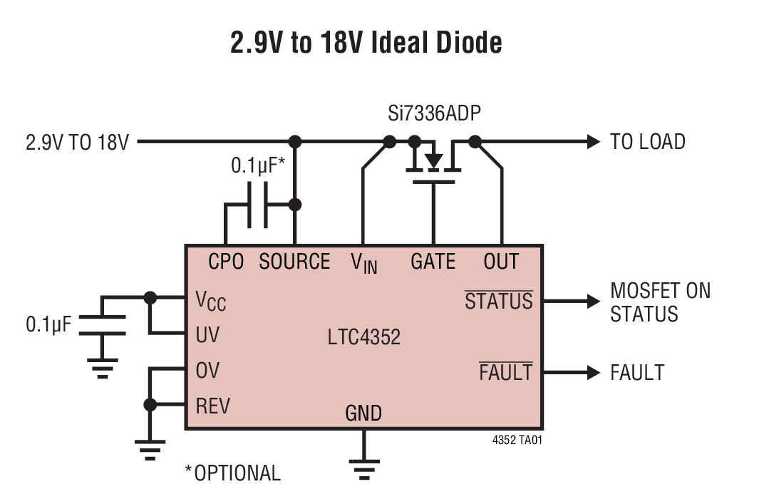
Analog Devices Inc.The LTC4352 creates a near-ideal diode using an external N-channel MOSFET. It replaces a high power Schottky diode and the associated heat sink, saving power and board area. The ideal diode function permits low loss power ORing and supply holdup applications. The LTC4352 regulates the forward voltage drop across the MOSFET to ensure smooth current transfer in diode-OR applications. A fast turn-on reduces the load voltage droop during supply switch-over. If the input supply fails or is shorted, a fast turn-off minimizes reverse currents. The controller operates with supplies from 2.9V to 18V. For lower voltages, an external supply is needed at the VCC pin. Power passage is disabled during undervoltage or overvoltage conditions. The controller also features an open MOSFET detect circuit that ?ags excessive voltage drop across the pass transistor in the on state. A REV pin enables reverse current, overriding the diode behavior when desired.Applications Redundant Power Supplies Supply Holdup Telecom Infrastructure Computer Systems and Servers

DC1332B-A
Analog Devices Inc.The LTC2631 is a family of 12-, 10-, and 8-bit voltage-output DACs with an integrated, high accuracy, low-drift reference in an 8-lead TSOT-23 package. It has a rail-to-rail output buffer that is guaranteed monotonic.The LTC2631-L has a full-scale output of 2.5V, and operates from a single 2.7V to 5.5V supply. The LTC2631-H has a full-scale output of 4.096V, and operates from a 4.5V to 5.5V supply. A 10ppm/?C reference output is available at the REF pin.Each DAC can also operate in External Reference mode, in which a voltage supplied to the REF pin sets the fullscale output.The LTC2631 DACs use a 2-wire, I2C-compatible serial interface. The LTC2631 operates in both the standard mode (clock rate of 100kHz) and the fast mode (clock rate of 400kHz).The LTC2631 incorporates a power-on reset circuit. Options are available for reset to zero-scale or reset to mid-scale after power-up.Applications Mobile Communications Process Control and Industrial Automation Automatic Test Equipment Portable Equipment Automotive Optical Networking
DC1332B-D
Analog Devices Inc.The LTC2631 is a family of 12-, 10-, and 8-bit voltage-output DACs with an integrated, high accuracy, low-drift reference in an 8-lead TSOT-23 package. It has a rail-to-rail output buffer that is guaranteed monotonic.The LTC2631-L has a full-scale output of 2.5V, and operates from a single 2.7V to 5.5V supply. The LTC2631-H has a full-scale output of 4.096V, and operates from a 4.5V to 5.5V supply. A 10ppm/?C reference output is available at the REF pin.Each DAC can also operate in External Reference mode, in which a voltage supplied to the REF pin sets the fullscale output.The LTC2631 DACs use a 2-wire, I2C-compatible serial interface. The LTC2631 operates in both the standard mode (clock rate of 100kHz) and the fast mode (clock rate of 400kHz).The LTC2631 incorporates a power-on reset circuit. Options are available for reset to zero-scale or reset to mid-scale after power-up.Applications Mobile Communications Process Control and Industrial Automation Automatic Test Equipment Portable Equipment Automotive Optical Networking


