
LTC6804-1 Demo Board | 12-Channel Battery Stack Monitor with Daisy-chain Interface
Analog Devices Inc.Demonstration circuit 1894B is a daisy-chainable isoSPI battery-stack monitor featuring the LTC6804-1. These boards can be linked through a 2-wire isolated serial interface to monitor any number of cells on a stack.

DC1908A-D
Analog Devices Inc.The LTC2328-18 is a low noise, high speed 18-bit successive approximation register (SAR) ADC with pseudo-differential inputs. Operating from a single 5V supply, the LTC2328-18 has a ?10.24V true bipolar input range, making it ideal for high voltage applications which require a wide dynamic range. The LTC2328-18 achieves ?5LSB INL maximum, no missing codes at 18 bits with 95dB SNR.The LTC2328-18 has an onboard single-shot capable reference buffer and low drift (20ppm/?C max) 2.048V temperature compensated reference. The LTC2328-18 also has a high speed SPI-compatible serial interface that supports 1.8V, 2.5V, 3.3V and 5V logic while also featuring a daisy-chain mode. The fast 1Msps throughput with no cycle latency makes the LTC2328-18 ideally suited for a wide variety of high speed applications. An internal oscillator sets the conversion time, easing external timing considerations. The LTC2328-18 dissipates only 50mW and automatically naps between conversions, leading to reduced power dissipation that scales with the sampling rate. A sleep mode is also provided to reduce the power consumption of the LTC2328-18 to 300?W for further power savings during inactive periods. Bits LTC2328-16 16 LTC2328-18 18 Applications Programmable Logic Controllers Industrial Process Control High Speed Data Acquisition Portable or Compact Instrumentation ATE

DC1908A-E
Analog Devices Inc.The LTC2327-18 is a low noise, high speed 18-bit successive approximation register (SAR) ADC with pseudo-differential inputs. Operating from a single 5V supply, the LTC2327-18 has a ?10.24V true bipolar input range, making it ideal for high voltage applications which require a wide dynamic range. The LTC2327-18 achieves ?5LSB INL maximum, no missing codes at 18 bits with 95dB SNR.The LTC2327-18 has an onboard single-shot capable reference buffer and low drift (20ppm/?C max) 2.048V temperature compensated reference. The LTC2327-18 also has a high speed SPI-compatible serial interface that supports 1.8V, 2.5V, 3.3V and 5V logic while also featuring a daisy-chain mode. The fast 500ksps throughput with no cycle latency makes the LTC2327-18 ideally suited for a wide variety of high speed applications. An internal oscillator sets the conversion time, easing external timing considerations. The LTC2327-18 dissipates only 36mW and automatically naps between conversions, leading to reduced power dissipation that scales with the sampling rate. A sleep mode is also provided to reduce the power consumption of the LTC2327-18 to 300?W for further power savings during inactive periods. Bits LTC2327-16 16 LTC2327-18 18 Applications Programmable Logic Controllers Industrial Process Control High Speed Data Acquisition Portable or Compact Instrumentation ATE
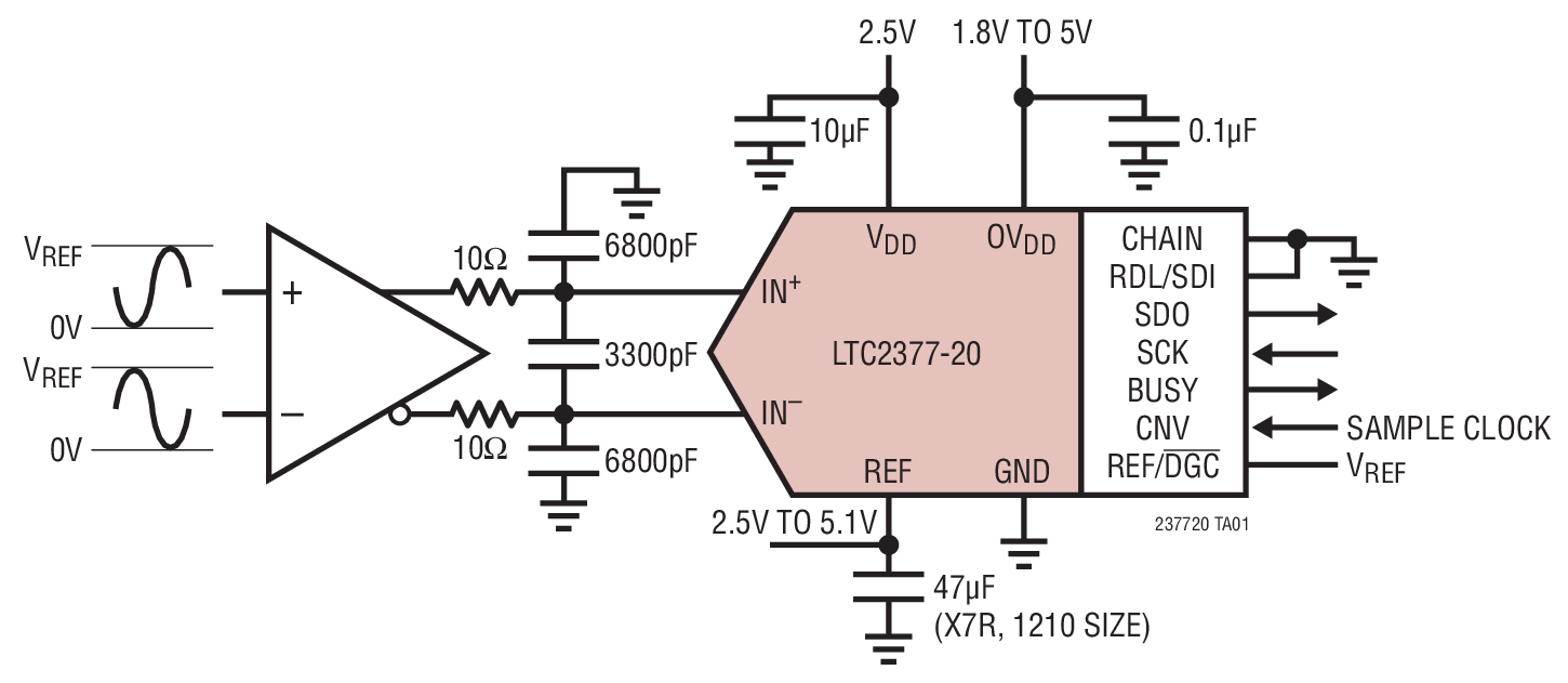
LTC2377-20 Demo Board | 20-Bit, 500ksps, SAR ADC with 104dB SNR. Requires DC2026
Analog Devices Inc.The LTC2378-20, LTC2377-20 and LTC2376-20 are 20‑bit, low power, low noise SAR ADCs with serial outputs that operate from a single 2.5V supply. The demo manual refers to the LTC2378-20 but applies to all parts in the family, the only difference being the maximum sample rate. The LTC2378-20 supports a ±5V fully differential input range with a 104dB SNR, consumes only 21mW and achieves ±2ppm INL max with no missing codes at 20 bits. The DC1925A demonstrates the DC and AC performance of the LTC2378-20 in conjunction with the DC590 QuikEval™ and DC890 PScope™ data collection boards. Use the DC590 to demonstrate DC performance such as peak-to-peak noise and DC linearity.

DC1930A
Analog Devices Inc.The LT3744 is a fixed frequency synchronous step-down DC/DC controller designed to drive a LED load at up to 20A continuous or 40A pulsed. The peak current mode controller will maintain ?3% LED current regulation over a wide output voltage range, from VEE to VIN. By allowing VEE to float to negative voltages, several LEDs in series can be driven from a single Li-Ion battery with a simple, single step-down output stage. PWM dimming is achieved with the PWM pins. The regulated LED current is set with analog voltages at the CTRL pins. Regulated voltage and overvoltage protection are set with a voltage divider from the output to the FB pin. The switching frequency is programmable from 100kHz to 1MHz through an external resistor on the RT pin.Additional features include an accurate external reference voltage, a control input for thermally derating regulation current, an accurate EN/UVLO pin, an open-drain output fault flag, OVLO, frequency synchronization, and thermal shutdown.Applications LED Driver for DLP Projectors Heads-Up Displays High Power LED

LT3072 Demo Board | Dual, Low Noise, 2.5A Programmable Output, Low Dropout Linear Regulator
Analog Devices Inc.Demonstration Circuit 1938A features the LT3072 dual, low noise, 2.5A programmable output, low dropout linear regulator. The input voltages VIN1 and VIN2 are independent and can range from 0.8V to 3.45V. Each channel has jumpers to set a three-bit code that determines output voltages VOUT1 and VOUT2 at pre-programmed levels with a range from 0.6V to 2.5V and a maximum output current of 2.5A. DC1938A requires a single external BIAS voltage that is higher than VIN1 and VIN2, between 2.375V and 5.25V and is at least 1.2V higher than the highest output voltage.
Each output is decoupled by a 1µF + 2.2µF + 6.8µF capacitor network and each input is decoupled with a 22µF capacitor. The internal reference of each channel is bypassed with a 0.1µF capacitor to reduce output noise and program the soft-start. 1500µF aluminum electrolytic capacitors and 220µF tantalum polymer capacitors hold up VIN1 and VIN2 but the aluminum electrolytic capacitors are cabling dependent and are not required on customer circuits. The BIAS voltage is bypassed at each channel’s BIAS pin with a 2.2µF capacitor and there is a single terminal for the BIAS input.
The positions of the VOUT1 and VOUT2 ENABLE jumpers either pull up the EN1 and EN2 pins to the BIAS voltage by a 100k resistor, short EN1 and EN2 to ground or float EN1 and EN2 so they can be driven directly by a signal applied to the EN1 and EN2 terminals. Each channel has a terminal for PWRGD that is pulled up to BIAS by a 51kΩ resistor. Resistors program a 3A output current limit and a 333mV/A output current monitoring voltage that is available at the IMON/LIM terminals. The TEMP terminal allows monitoring of die temperature.
VOIC allows automatic control of a pre-regulation voltage and the VOIC pins are bypassed with 1nF capacitors. MARGA1 and MARGA2 terminals for margining allow an
optional external voltage to program an adjustment to each channel’s output voltage.
Banana jacks minimize voltage drops on VIN and VOUT connections. Each channel’s SENSE pin terminates at a 10µF capacitor near the VOUT banana jacks. The PCB design minimizes parasitic SENSE to GND and SENSE to OUT trace capacitance. VO1+, VO1-, VO2+ and VO2- terminals Kelvin-connect to the 10µF VOUT capacitors and are the optimal place to observe output voltage regulation and load transient response. Each output has a 560Ω pre-load so the minimum load requirement is met over the VOUT programming range.
DC1938A has placeholders identified on the schematic as optional (Opt) components that make it convenient to add capacitance, add filtering, parallel references or use the VOIC function – check the schematic for placeholder locations.
The LT3072 is well suited to microprocessor systems and instrumentation applications with stringent performance requirements for output noise and load transient response. Systems with high efficiency requirements will benefit from the low dropout of the LT3072. DC1938A features the LT3072 in a thermally enhanced 36-lead 4mm × 7mm QFN package. The LT3072 data sheet must be read in conjunction with this demo manual to properly use or modify demo circuit DC1938A.

DC1941D
Analog Devices Inc.The LTC6820 provides bidirectional SPI communications between two isolated devices through a single twisted-pair connection. Each LTC6820 encodes logic states into signals that are transmitted across an isolation barrier to another LTC6820. The receiving LTC6820 decodes the transmission and drives the slave bus to the appropriate logic states. The isolation barrier can be bridged by a simple pulse transformer to achieve hundreds of volts of isolation.The LTC6820 drives differential signals using matched source and sink currents, eliminating the requirement for a transformer center tap and reducing EMI. Precision window comparators in the receiver detect the differential signals. The drive currents and the comparator thresholds are set by a simple external resistor divider, allowing the system to be optimized for required cable lengths and desired signal-to-noise performance.Applications Industrial Networking Battery Monitoring Systems Remote Sensors

LTC2185 and LTC6409 Combo Board with differential inputs, requires DC890, LVDS_XFMR and DC1075
Analog Devices Inc.DC1945A: Demo Board for the LTC2185 - 16-Bit, 125Msps Low Power Dual ADCs and LTC6409 - 10GHz GBW, 1.1nV/√Hz Differential Amplifier/ADC Driver.

DC1954A-D
Analog Devices Inc.The LTC6954 is a family of very low phase noise clock distribution parts. Each part has three outputs and each output has an individually programmable frequency divider and delay. There are four members of the family, differing in their output logic signal type:LTC6954-1: Three LVPECL outputsLTC6954-2: Two LVPECL and one LVDS/CMOS outputsLTC6954-3: One LVPECL and two LVDS/CMOS outputsLTC6954-4: Three LVDS/CMOS outputsEach output is individually programmable to divide the input frequency by any integer from 1 to 63, and to delay each output by 0 to 63 input clock cycles. The output duty cycle is always 50%, regardless of the divide number. The LVDS/CMOS outputs are jumper selectable via the OUTxSEL pins to provide either an LVDS logic output or a CMOS logic output.The LTC6954 also features Linear Technology?s EZSync system for perfect clock synchronization and alignment every time.All device settings are controlled through an SPI-compatible serial port.Applications Clocking High Speed, High Resolution ADCs, DACs?and Data Acquisition Systems Low Jitter Clock Distribution

DC1956A
Analog Devices Inc.The LT3905 is a fixed frequency current-mode step-up converter designed to bias avalanche photodiodes (APD) in optical receivers. The LT3905 features high side APD current monitoring over four decades of dynamic range with better than 2% relative accuracy over the 3?A to 3mA range.The maximum APD current is programmed with a single resistor, and a fast current limiter with indicator protects the APD during overload conditions. Adjustable output voltage provides dynamic bias control, and an adjustable loss-of-signal indicator flags low APD current.Coupled with the integrated DMOS power switch and Schottky rectifier, the LT3905 provides a compact total solution with few external components and low solution cost. Constant switching frequency results in predictable output noise that is easy to filter.The LT3905 is available in the tiny footprint (3mm ? 3mm) 16-Lead QFN Package.Applications APD Bias PIN Diode Bias Optical Receivers and Modules Fiber Optic Network Equipment

DC1961A
Analog Devices Inc.The LT3748 is a switching regulator controller specifically designed for the isolated flyback topology and capable of high power. It drives a low side external N-channel power MOSFET from an internally regulated 7V supply. No third winding or opto-isolator is required for regulation as the part senses the isolated output voltage directly from the primary-side flyback waveform.The LT3748 utilizes boundary mode to provide a small magnetic solution without compromising load regulation. Operating frequency is set by load current and transformer magnetizing inductance. The gate drive of the LT3748 combined with a suitable external MOSFET allow it to deliver load power up to several tens of watts from input voltages as high as 100V.The LT3748 is available in a high voltage 16-lead MSOP package with four leads removed.APPLICATIONS Isolated Telecom Converters High Power Automotive Supplies Isolated Industrial Power Supplies Military and High Temperature Applications

Starter Kit for Power System Management [Includes DC1962C, DC1613A]
Analog Devices Inc.DC1962C-KIT Demo Board for:
LTC2977 8-Channel PMBus Power System Manager Featuring Accurate Output Voltage Measurement
LTC2974 4-Channel PMBus Power System Manager Featuring Accurate Output Current Measurement
LTC3880 Dual Output PolyPhase Step-Down DC/DC Controller with Digital Power System Management

LT8697 Demo Board | 6V ≤ VIN ≤ 42V, 5V @ 2.5A USB Supply Output, Cable Drop Compensation
Analog Devices Inc.Demonstration circuit 1973A is a USB 5V 2.5A output, 6V to 42V input synchronous buck with cable drop compensation featuring the LT8697. The LT8697 is a compact, high efficiency, high speed synchronous monolithic step-down switching regulator designed to power 5V USB applications. A precise output voltage and programmable cable drop compensation maintain accurate 5V regulation at the USB socket at the end of a long cable. The circuit runs at 2MHz to minimize external components size and to avoid AM band.

DC1974A-B
Analog Devices Inc.The LTC2123 is a 2-channel simultaneous sampling 250Msps 14-bit A/D converter with serial JESD204B outputs. It is designed for digitizing high frequency, wide dynamic range signals. It is perfect for demanding communications applications with AC performance that includes 70dBFS SNR and 90dBFS spurious free dynamic range (SFDR). The 1.25GHz input bandwidth allows the ADC to under-sample high frequencies.The 5Gbps JESD204B serial interface simplifies the PCB design by minimizing the number of data lines required.The DEVCLK+ and DEVCLK? inputs can be driven differentially with sine wave, PECL, or LVDS signals. An optional clock divide-by-two circuit or clock duty cycle stabilizer maintains high performance at full speed for a wide range of clock duty cycles.Applications Communications Cellular Base Stations Software Defined Radios Medical Imaging High Definition Video Test and Measurement Instrumentation

DC1986A
Analog Devices Inc.The LTM2892 is a complete galvanic digital ?Module? (micromodule) isolator. No external components are required. Individual 3V to 5.5V supplies power each side of the digital isolator. Separate logic supply pins allow easy interfacing with different logic levels from 1.62V to 5.5V, independent of the main supply.Module options are available with compatibility to SPI (LTM2892-S) and I2C (LTM2892-I), master mode only, specifications.Coupled inductors provide 3500VRMS of isolation between the input and output logic interface. This device is ideal for systems where the ground loop is broken, allowing uninterrupted communication through large common mode transients faster than 50kV/?s.Applications Isolated SPI or I2C Interfaces Industrial Systems Test and Measurement Equipment Breaking Ground Loops

DC1987A
Analog Devices Inc.The LTM8057 is a 2kV AC isolated flyback ?Module? (power module) DC/DC converter. Included in the package are the switching controller, power switches, transformer, and all support components. Operating over an input voltage range of 3.1V to 31V, the LTM8057 supports an output voltage range of 2.5V to 12V, set by a single resistor. Only output and input capacitors are needed to finish the design. Other components may be used to control the soft-start control and biasing.The LTM8057 is packaged in a thermally enhanced, compact (9mm ? 11.25mm ? 4.92mm) overmolded ball grid array (BGA) package suitable for automated assembly by standard surface mount equipment. The LTM8057 is available with SnPb or RoHS compliant terminal finish.Applications Industrial Sensors Industrial Switches Test and Measurement Equipment

DC1992A
Analog Devices Inc.The LT8620 is a compact, high efficiency, high speed synchronous monolithic step-down switching regulator that accepts a wide input voltage range up to 65V, and consumes only 2.5?A of quiescent current. Top and bottom power switches are included with all necessary circuitry to minimize the need for external components. Low ripple Burst Mode operation enables high efficiency down to very low output currents while keeping the output ripple below 10mVP-P. A SYNC pin allows synchronization to an external clock. Internal compensation with peak current mode topology allows the use of small inductors and results in fast transient response and good loop stability. The EN/UV pin has an accurate 1V threshold and can be used to program VIN undervoltage lockout or to shut down the LT8620 reducing the input supply current to 1?A. A capacitor on the TR/SS pin programs the output voltage ramp rate during start-up. The PG flag signals when VOUT is within ?9% of the programmed output voltage as well as fault conditions. The LT8620 is available in small 16-Lead MSOP and 3mm ? 5mm QFN packages with exposed pads for low thermal resistance.Applications Automotive and Industrial Supplies General Purpose Step-Down GSM Power Supplies

DC1996A-A
Analog Devices Inc.The LTC2323-16 is a low noise, high speed dual 16- bit successive approximation register (SAR) ADC with differential inputs and wide input common mode range. Operating from a single 3.3V or 5V supply, the LTC2323-16 has an 8VP-P differential input range, making it ideal for applications which require a wide dynamic range with high common mode rejection. The LTC2323-16 achieves ?4LSB INL typical, no missing codes at 16 bits and 81dB SNR.The LTC2323-16 has an onboard low drift (20ppm/?C max) 2.048V or 4.096V temperature-compensated reference. The LTC2323-16 also has a high speed SPI-compatible serial interface that supports CMOS or LVDS. The fast 5Msps per channel throughput with one-cycle latency makes the LTC2323-16 ideally suited for a wide variety of high speed applications. The LTC2323-16 dissipates only 40mW per channel and offers nap and sleep modes to reduce the power consumption to 5?W for further power savings during inactive periods. Bits LTC2323-12 12 LTC2323-14 14 LTC2323-16 16 Applications High Speed Data Acquisition Systems Communications Remote Data Acquisition Imaging Optical Networking Automotive Multiphase Motor Control

DC1996A-B
Analog Devices Inc.The LTC2321-16 is a low noise, high speed dual 16-bit successive approximation register (SAR) ADC with differential inputs and wide input common mode range. Operating from a single 3.3V or 5V supply, the LTC2321-16 has an 8VP-P differential input range, making it ideal for applications which require a wide dynamic range with high common mode rejection. The LTC2321-16 achieves ?4LSB INL typical, no missing codes at 16 bits and 81dB SNR.The LTC2321-16 has an on-board low drift (20ppm/?C max) 2.048V or 4.096V temperature-compensated reference. The LTC2321-16 also has a high speed SPI-compatible serial interface that supports CMOS or LVDS. The fast 2Msps per channel throughput with no cycle latency makes the LTC2321-16 ideally suited for a wide variety of high speed applications. The LTC2321-16 dissipates only 31mW per channel and offers nap and sleep modes to reduce the power consumption to 5?W for further power savings during inactive periods. Bits LTC2321-12 12 LTC2321-14 14 LTC2321-16 16 Applications High Speed Data Acquisition Systems Communications Remote Data Acquisition Imaging Optical Networking Automotive Multiphase Motor Control

DC1996A-D
Analog Devices Inc.The LTC2321-14 is a low noise, high speed dual 14-bit + sign successive approximation register (SAR) ADC with differential inputs and wide input common mode range. Operating from a single 3.3V or 5V supply, the LTC2321-14 has an 8VP-P differential input range, making it ideal for applications which require a wide dynamic range with high common mode rejection. The LTC2321-14 achieves ?1LSB INL typical, no missing codes at 14 bits and 80dB SNR.The LTC2321-14 has an on-board low drift (20ppm/?C max) 2.048V or 4.096V temperature-compensated reference. The LTC2321-14 also has a high speed SPI-compatible serial interface that supports CMOS or LVDS. The fast 2Msps per channel throughput with no-cycle latency makes the LTC2321-14 ideally suited for a wide variety of high speed applications. The LTC2321-14 dissipates only 33mW per channel and offers nap and sleep modes to reduce the power consumption to 5?W for further power savings during inactive periods. Bits LTC2321-12 12 LTC2321-14 14 LTC2321-16 16 Applications High Speed Data Acquisition Systems Communications Remote Data Acquisition Imaging Optical Networking Automotive Multiphase Motor Control


