EV1HMC787ALC3B
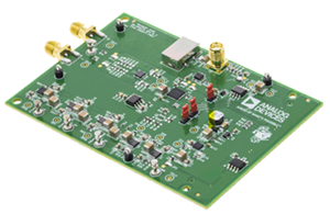
Analog Devices Inc.HMC787ALC3BThe HMC787A is a general-purpose, double balanced mixer in a 12-terminal, RoHS compliant, ceramic leadless chip carrier (LCC) package that can be used as an upconverter or down- converter from 3 GHz to 10 GHz. This mixer is fabricated in a gallium arsenide (GaAs), metal semiconductor field effect transistor (MESFET) process and requires no external components or matching circuitry. The HMC787A provides excellent local oscillator (LO) to radio frequency (RF) and LO to intermediate frequency (IF) isolation due to optimized balun structures and operates with a LO drive level of 17 dBm. The ceramic LCC package eliminates the need for wire bonding and is compatible with high volume, surface-mount manufacturing techniques.HMC787AG (CHIP)The HMC787AG is a general-purpose, double balanced mixer that can be used as an upconverter or downconverter from 3 GHz to 10 GHz. This mixer is fabricated in a gallium arsenide (GaAs), metal semiconductor field effect transistor (MESFET) process and requires no external components or matching circuitry. The HMC787AG provides high local oscillator (LO) to RF and LO to intermediate frequency (IF) isolation due to optimized balun structures and operates with a LO drive level between 13 dBm to 21 dBm.Applications Microwave Radio Industrial, scientific, and medical (ISM) band and ultrawide band (UWB) radio Test equipment & sensors Military end use
EV1HMC792ALP4
Analog Devices Inc.The HMC792ALP4E is a broadband 6-bit GaAs IC Digital Attenuator in a low cost leadless SMT package. This versatile digital attenuator incorporates off-chip AC ground capacitors for near DC operation, making it suitable for a wide variety of RF and IF applications. The dual mode control interface is CMOS/TTL compatible, and accepts either a three wire serial input or a 6 bit parallel word. The HMC792ALP4E also features a user selectable power up state and a serial output port for cascading other Hittite serial controlled components. The HMC792ALP4E is housed in a RoHS compliant 4x4 mm QFN leadless package, and requires no external matching components.Applications Cellular/3G infrastructure WiBro / WiMAX / 4G Microwave radio & VSAT Test equipment and sensors IF & RF applications
EV1HMC8038LP4C
Analog Devices Inc.The HMC8038 is a high isolation, nonreflective, 0.1 GHz to 6.0 GHz, silicon, single-pole, double-throw (SPDT) switch in a leadless, surface-mount package. The switch is ideal for cellular infrastructure applications, yielding up to 62 dB of isolation up to 4.0 GHz, a low 0.8 dB of insertion loss up to 4.0 GHz, and 60 dBm of input third-order intercept. Power handling is excellent up to 6.0 GHz, and it offers an input power for an 0.1 dB compression point (P0.1dB) of 35 dBm (VDD = 5 V). On-chip circuitry operates a single, positive supply voltage from 3.3 V to 5 V, as well as a single, positive voltage control from 0 V to 1.8 V/3.3 V/5.0 V at very low dc currents. An enable input (EN) set to logic high places the switch in an all off state, in which RFC is reflective.The HMC8038 has ESD protection on all device pins, including the RF interface, and can stand 4 kV HMB and 1.25 kV CDM. The HMC8038 offers very fast switching and RF settling times of 150 ns and 170 ns, respectively. The device comes in a RoHS-compliant, compact 4 mm ? 4 mm LFCSP package.Applications Cellular/4G infrastructure Wireless infrastructure Automotive telematics Mobile radios Test equipment
EV1HMC890ALP5
Analog Devices Inc.The HMC890ALP5E is a monolithic microwave integratedcircuit (MMIC), band-pass filter that features a user selectablepass-band frequency. The 3 dB filter bandwidth is approximately 10%. The ?20 dB filter bandwidth is approximately 30%. Thecenter frequency can vary between 1.0 GHz and 1.9 GHz by applying an analog tuning voltage between 0 V and 14 V. This tunable filter can be used as a much smaller alternative to physically large switched filter banks and cavity tuned filters.The HMC890ALP5E has excellent microphonics due to themonolithic design, and provides a dynamically adjustablesolution in advanced communications applications.APPLICATIONS Test and measurement equipment Military radar and electronic warfare/electronic countermeasures Satellite communications and space Industrial and medical equipment
EV1HMC907APM5
Analog Devices Inc.The HMC907APM5E is a GaAs MMIC pHEMT Distributed Power Amplifier which operates between 0.2 and 22 GHz. This self-biased power amplifier provides 14 dB of gain, +40 dBm output IP3 and +28 dBm of output power at 1 dB gain compression while requiring only 350 mA from a +10 V supply. Gain flatness is excellent at ?0.7 dB from 0.2 to 22 GHz making the HMC907APM5E ideal for EW, ECM, Radar and test equipment applications. The HMC907APM5E amplifier I/Os are internally matched to 50 ? facilitatingintegration into Mutli-Chip-Modules (MCMs) and is packaged in a leadless QFN 5x5 mm surface mount package, and requires no external matching components.Applications Test instrumentation Military & space
EV1HMC985ALP4K
Analog Devices Inc.The HMC985ALP4KE is an absorptive VoltageVariable Attenuator (VVA) which operates from 10- 40 GHz and is ideal in designs where an analogDC control signal must be used to control RF signallevels over a 35 dB dynamic range. It features twoshunt-type attenuators which are controlled by twoanalog voltages, Vctl1 and Vctl2. Optimum linearityperformance of the attenuator is achieved by firstvarying Vctl1 of the first attenuation stage from -5V to0V with Vctl2 fixed at -5V. The control voltage of thesecond attenuation stage, Vctl2, should then be variedfrom -5V to 0V with Vctl1 fixed at 0V.If the Vctl1 and Vctl2 pins are connected together it ispossible to achieve the full analog attenuation rangewith only a small degradation in input IP3 performance.Applications include AGC circuits and temperaturecompensation of multiple gain stages in microwavepoint-to-point and VSAT radios.Applications Point-to-Point Radio VSAT Radio Test Instrumentation Microwave Sensors Military, ECM & Radar
EV1HMC994APM5
Analog Devices Inc.The HMC994APM 5E is a GaAs pHEMT MMIC Distributed Wideband Power Amplifier which operates between DC and 28 GHz. The amplifier provides 15 dB of gain, +29 dBm of saturated output power, and 25% PAE from a +10V supply. With up to +38 dBm Output IP 3 the HMC994APM 5E is ideal for high linearity applications in military and space as well as test equipment where high order modulations are used. The HMC994APM 5E exhibits a positive gain slope from 2 to 20 GHz making it ideal for EW , ECM,and test equipment applications. The HMC994APM5E amplifier I/Os are internally matched to 50 Ohms and is packaged in a leadless QFN 5x5 mm surface mount package.Applications Test Instrumentation Military & Space Fiber optics
EV-AD74412RSDZ
Analog Devices Inc.The AD74412R is a quad-channel software configurable input/output solution for building and process control applications. The AD74412R contains functionality for analog output, analog input, digital input, and resistance temperature detector (RTD) measurements integrated into a single chip solution with an interface compatible with the serial port interface (SPI).The device features a 16-bit, ?-? analog-to-digital converter (ADC) and four configurable, 13-bit digital-to-analog converters (DACs) to provide four configurable input/output channels and a suite of diagnostic functions.There are several modes related to the AD74412R. These modes are voltage output, current output, voltage input, externally powered current input, loop powered current input, external RTD measurement, digital input logic, and loop powered digital input.The AD74412R contains a high accuracy 2.5 V internal reference to drive the DACs and the ADC.Product Highlights Quad-Channel, Software Configurable Channels. Built In Diagnostics and Alert Features. Robust Architecture. Surge tested to ?1 kV, per the IEC61000-4-5 standard, on the input/output terminals with unshielded cables.?Applications? Building control systems Process control Industrial automation ?
EV-ADA4571RSDZ
Analog Devices Inc.The ADA4571 is an anisotropic magnetoresistive (AMR) sensorwith integrated signal conditioning amplifiers and ADC drivers.The ADA4571 produces two analog outputs that indicate theangular position of the surrounding magnetic field.The ADA4571 consists of two die within one package, an AMRsensor, and a fixed gain (G = 40 nominally) instrumentationamplifier. The ADA4571 delivers clean and amplified cosineand sine output signals related to the angle of a rotatingmagnetic field. The output voltage range is ratiometric to thesupply voltage.The sensor contains two Wheatstone bridges, at a relative angleof 45? to one another. A rotating magnetic field in the x-ysensor plane delivers two sinusoidal output signals with thedouble frequency of the angle (?) between sensor and magneticfield direction. Within a homogeneous field in the x-y plane,the output signals are independent of the physical placement inthe z direction (air gap).The ADA4571 is available in an 8-lead SOIC package.Product Highlights Contactless angular measurement. Measures magnetic field direction rather than field intensity. Minimum sensitivity to air gap variations. Large working distance. Excellent accuracy, even for weak saturation fields. Minimal thermal and lifetime drift. Negligible hysteresis. Single chip solution.Applications Absolute position measurement (linear and angle) Brushless dc motor control and positioning Actuator control and positioning Contactless angular measurement and detection Magnetic angular position sensing
EV-ADE9000SHIELDZ
Analog Devices Inc.The ADE9000 is a highly accurate, fully integrated, multiphase energy and power quality monitoring device. Superior analog performance and a digital signal processing (DSP) core enable accurate energy monitoring over a wide dynamic range. An integrated high end reference ensures low drift over temperature with a combined drift of less than ?25 ppm/?C maximum for the entire channel including a programmable gain amplifier (PGA) and an analog-to-digital converter (ADC).The ADE9000 offers complete power monitoring capability by providing total as well as fundamental measurements on rms, active, reactive, and apparent powers and energies. Advanced features such as dip and swell monitoring, frequency, phase angle, voltage total harmonic distortion (VTHD), current total harmonic distortion (ITHD), and power factor measurements enable implementation of power quality measurements. The ? cycle rms and 10 cycle rms/12 cycle rms, calculated according to IEC 61000-4-30 Class S, provide instantaneous rms measurements for real-time monitoring.The ADE9000 offers an integrated flexible waveform buffer that stores samples at a fixed data rate of 32 kSPS or 8 kSPS, or a sampling rate that varies based on line frequency to ensure 128 points per line cycle. Resampling simplifies fast Fourier transform (FFT) calculation of at least 50 harmonics in an external processor.The ADE9000 simplifies the implementation of energy and power quality monitoring systems by providing tight integration of acquisition and calculation engines. The integrated ADCs and DSP engine calculate various parameters and provide data through user accessible registers or indicate events through interrupt pins. With seven dedicated ADC channels, the ADE9000 can be used on a 3-phase system or up to three single-phase systems. It supports current transformers (CTs) or Rogowski coils for current measurements. A digital integrator eliminates a discrete integrator required for Rogowski coils.The ADE9000 absorbs most complexity in calculations for a power monitoring system. With a simple host microcontroller, the ADE9000 enables the design of standalone monitoring or protection systems, or low cost nodes uploading data into the cloud.Note that throughout this data sheet, multifunction pins, such as CF4/EVENT/DREADY, are referred to either by the entire pin name or by a single function of the pin, for example, EVENT, when only that function is relevant.Applications Energy and power monitoring Power quality monitoring Protective devices Machine health Smart power distribution units Polyphase energy meters
EV-ADF41513SD1Z
Analog Devices Inc.The ADF41513 is an ultralow noise frequency synthesizer that can be used to implement local oscillators (LOs) as high as 26.5 GHz in the upconversion and downconversion sections of wireless receivers and transmitters.The ADF41513 is designed on a high performance silicon geranium (SiGe), bipolar complementary metal-oxide semiconductor (BiCMOS) process, achieving a normalized phase noise floor of ?235 dBc/Hz. The phase frequency detector (PFD) operates up to 250 MHz (integer N mode)/125 MHz (fractional-N mode) for improved phase noise and spur performance. The variable modulus, ?-? modulator allows extremely fine resolution when using a 49-bit divide value. The ADF41513 can be used as an integer N phase-locked loop (PLL), or it can be used as a fractional-N PLL with either a fixed modulus for subhertz frequency resolution or variable modulus for subhertz exact frequency resolution.A complete PLL is implemented when the synthesizer is used with an external loop filter and voltage controlled oscillator (VCO). The 26.5 GHz bandwidth eliminates the need for a frequency doubler or divider stage, simplifying system architecture and reducing cost. The ADF41513 is packaged in a compact, 24-lead, 4 mm ? 4 mm LFCSPApplications Test equipment and instrumentation Wireless infrastructure Microwave point to point and multipoint radios Very small aperture terminal (VSAT) radios Aerospace and defense
EV-ADF41513SD3Z
Analog Devices Inc.The ADF41513 is an ultralow noise frequency synthesizer that can be used to implement local oscillators (LOs) as high as 26.5 GHz in the upconversion and downconversion sections of wireless receivers and transmitters.The ADF41513 is designed on a high performance silicon geranium (SiGe), bipolar complementary metal-oxide semiconductor (BiCMOS) process, achieving a normalized phase noise floor of ?235 dBc/Hz. The phase frequency detector (PFD) operates up to 250 MHz (integer N mode)/125 MHz (fractional-N mode) for improved phase noise and spur performance. The variable modulus, ?-? modulator allows extremely fine resolution when using a 49-bit divide value. The ADF41513 can be used as an integer N phase-locked loop (PLL), or it can be used as a fractional-N PLL with either a fixed modulus for subhertz frequency resolution or variable modulus for subhertz exact frequency resolution.A complete PLL is implemented when the synthesizer is used with an external loop filter and voltage controlled oscillator (VCO). The 26.5 GHz bandwidth eliminates the need for a frequency doubler or divider stage, simplifying system architecture and reducing cost. The ADF41513 is packaged in a compact, 24-lead, 4 mm ? 4 mm LFCSPApplications Test equipment and instrumentation Wireless infrastructure Microwave point to point and multipoint radios Very small aperture terminal (VSAT) radios Aerospace and defense
EV-ADF4157SD1Z
Analog Devices Inc.The ADF4157 is a 6 GHz fractional-N frequency synthesizer with a 25-bit fixed modulus, allowing subhertz frequency resolution at 6 GHz. It consists of a low noise digital phase frequency detector (PFD), a precision charge pump, and a programmable reference divider. There is a ?-? based fractional interpolator to allow programmable fractional-N division. The INT and FRAC values define an overall N divider, N = INT + (FRAC/225). The ADF4157 features cycle slip reduction circuitry, which leads to faster locktimes without the need for modifications to the loop filter.Control of all on-chip registers is via a simple 3-wire interface.The device operates with a power supply ranging from 2.7 V to3.3 V and can be powered down when not in use.ApplicationsSatellite communications terminals, radar equipmentInstrumentation equipmentPersonal mobile radio (PMR)Base stations for mobile radioWireless handsets
EV-ADF4355-3SD1Z
Analog Devices Inc.The ADF4355-3 allows the implementation of fractional-N orinteger-N phase-locked loop (PLL) frequency synthesizers whenused with an external loop filter and an external referencefrequency. A series of frequency dividers at the output provideoperation from 51.5625 MHz to 6600 MHz.The ADF4355-3 has an integrated VCO with a fundamentaloutput frequency ranging from 3300 MHz to 6600 MHz. Inaddition, the VCO frequency is connected to divide by 1, 2, 4, 8,16, 32, or 64 circuits that allow the user to generate RF outputfrequencies as low as 51.5625 MHz. For applications that requireisolation, the RF output stage can be muted. The mute functionis both pin- and software-controllable.Control of all on-chip registers is through a simple 3-wire interface.The ADF4355-3 operates with analog, digital, charge pump, andVCO power supplies ranging from 3.1515 V to 3.4485 V. TheADF4355-3 also contains hardware and software power-downmodes.Applications Wireless infrastructure (W-CDMA, TD-SCDMA, WiMAX, GSM, PCS, DCS, DECT) Point to point/point to multipoint microwave links Satellites/VSATs Test equipment/instrumentation Clock generation
EV-ADF5356SD1Z
Analog Devices Inc.The ADF5356 allows implementation of fractional-N or integer Nphase-locked loop (PLL) frequency synthesizers when used with an external loop filter and an external reference frequency. Thewideband microwave VCO design permits frequency operationfrom 6.8 GHz to 13.6 GHz at one radio frequency (RF) output. A series of frequency dividers at another frequency output permitsoperation from 53.125 MHz to 6800 MHz. The ADF5356 has an integrated VCO with a fundamental output frequency ranging from 3400 MHz to 6800 MHz. In addition, the VCO frequency is connected to divide by 1, 2, 4, 8,16, 32, or 64 circuits that allow the user to generate RF output frequencies as low as 53.125 MHz. For applications that requireisolation, the RF output stage can be muted. The mute functionis both pin- and software-controllable. Control of all on-chip registers is through a simple 3-wire interface.The ADF5356 operates with analog and digital power suppliesranging from 3.15 V to 3.45 V, with charge pump and VCOsupplies from 4.75 V to 5.25 V. The ADF5356 also containshardware and software power-down modes.Applications Wireless infrastructure (LTE, W-CDMA, TD-SCDMA, WiMAX, GSM, PCS, DCS) Point to point and point to multipoint microwave links Satellites and very small aperture terminals (VSATs) Test equipment and instrumentation Clock generation
EV-ADF70301-915AZ
Analog Devices Inc.The ADF7030-1 is a fully integrated, radio transceiver achieving high performance at very low power. The ADF7030-1 is ideally suited for applications that require long range, network robustness, and long battery life. It is suitable for applications that operate in the ISM, SRD, and licensed frequency bands at 169.4 MHz to 169.6 MHz, 426 MHz to 470 MHz, and 863 MHz to 960 MHz. It provides extensive support for standards-based protocols like IEEE802.15.4g while also providing flexibility to support a wide range of proprietary protocols.The highly configurable low intermediate frequency (IF) receiver supports a large range of receiver channel bandwidths from 2.6 kHz to 406 kHz. This range of receiver channel bandwidths allows the ADF7030-1 to support ultranarrow-band, narrow-band, and wideband channel spacing.The ADF7030-1 features two independent PAs supporting output power ranges of ?20 dBm to +13 dBm and ?20 dBm to +17 dBm. The PAs support ultrafine adjustment of the power with a step resolution of 0.1 dB. The PA output power is exceptionally robust over temperature and voltage. The PAs have an automatic power ramp control to limit spectral splatter to meet regulatory standards.The ADF7030-1 features an on-chip ARM??Cortex?-M0 processor that performs radio control, radio calibration, and packet management. Cortex-M0 eases the processing burden of the host processor because the ADF7030-1 integrates the lower layers of a typical communication protocol stack. This internal processor also permits the download and execution of Analog Devices, Inc., provided firmware modules that can extend the functionality of the ADF7030-1.The ADF7030-1 has two packet modes: generic packet mode and IEEE802.15.4g mode. In generic packet mode, the packet format is highly flexible and fully programmable, thereby ensuring its compatibility with proprietary packet formats. In IEEE802.15.4g packet mode, the packet format conforms to the?IEEE802.15.4g standard. FEC, as per the IEEE802.15.4g standard, is also supported.The ADF7030-1 operates with a power supply range of 2.2 V to 3.6 V and has very low power consumption in both Tx and Rx modes, enabling long lifetimes in battery-operated systems. An ultralow power deep sleep mode achieves a typical current of 10 nA with the configuration memory retained.A complete wireless solution can be built using a small number of external discrete components and a host processor (typically a microcontroller). The host processor can configure the ADF7030-1 using a simple command-based protocol over a standard 4-wire SPI interface. A single-byte command transitions the radio between states or performs a radio function.The ADF7030-1 is available in two package types: a 6 mm ? 6 mm, 40-lead LFCSP and a 7 mm ? 7 mm, 48-lead LQFP. Both package types use NiPdAu plating to mitigate against silver migration in high humidity applications. The ADF7030-1 operating temperature range is ?40?C to +85?C.For Figure 13 to Figure 19, Figure 30, Figure 42, Figure 60, Figure 61, and Figure 75 in the Typical Performance Characteristics section, PA_COARSE is a programmable value that provides a coarse adjustment of the PA output power. This value can be programmed in the range of 1 to 6 for PA1, and from 1 to 10 for PA2. PA_FINE is a programmable value that provides a fine adjustment of the PA output power. This value can be programmed in the range of 3 to 127 for both PA1 and PA2. PA_MICRO is a programmable value that provides a microadjustment (typically
EV-ADL5335SD1Z
Analog Devices Inc.The ADL5335 is a digital gain amplifier (DGA) optimized foruse in wireless transmitters. A differential input and single-ended output facilitates a balun free connection between thebroadband integrated transceivers with differential outputs andthe RF gain blocks and drivers amplifiers with single-ended inputs.The gain is programmable via a standard Analog Devices, Inc.,serial peripheral interface (SPI) port from a maximum gain of 12.0 dB down to a minimum gain of ?8.0 dB with a gain stepsize of 0.5 dB. The ADL5335 also features a fast attack functionwhere the gain can rapidly increase or decrease by theapplication of a single pulse.The use of a thermometer-based digital step attenuator (DSA)ensures that gain changes are fundamentally glitch free. TheADL5335 is packaged in a 4 mm ? 4 mm, 16-lead LFCSP. Afully populated evaluation board and system demonstrationplatform (SDP)-based control software are available.Applications RF power control and calibration in wireless transmitters
EV-ADRF6658SD1Z
Analog Devices Inc.The ADRF6658 is a high performance, low power, wideband, dual-channel radio frequency (RF) downconverter with integrated intermediate frequency (IF) digitally controlled amplifiers (DGAs) for wideband, low distortion base station radio receivers.The dual Rx mixers are doubly balanced Gilbert cell mixers with high linearity and excellent image rejection. Both mixers convert 50 ? RF inputs to open-collector broadband IF outputs. Internal tunable baluns on the RF inputs enable suppression of RF signal harmonics and attenuation of out-of-band signals before the mixer inputs, reducing input reflections and out-of-band interference signals. A flexible local oscillator (LO) architecture allows the use of differential or single-ended LO signals.The dual-channel IF DGAs are based on the ADL5201 and ADL5202 and have a fixed, differential output impedance of 100 ?. The gain is adjustable over a 31.5 dB range with a 0.5 dB step size via the on-chip SPI, or through independent, 6-bit parallel ports that support latch functionality. Each channel, from the mixer inputs to the IF amplifier outputs, together with an LC interstage band-pass filter, achieves a maximum voltage conversion gain of 26.5 dB.Fabricated with the Analog Devices, Inc., high speed SiGe process, the ADRF6658 is available in a compact, 7 mm ? 7 mm, 48-lead LFCSP package, and operates over the ?40?C to +105?C temperature range.APPLICATIONS Cellular base stations and wireless infrastructure receivers (W-CDMA, TD-SCDMA, WiMAX, GSM, LTE, PCS, DCS, DECT) Active antenna systems PTP radio link down converters Wireless LANs and CATV equipment
EV-ADUCM322QSPZ
Analog Devices Inc.The ADuCM322 is a fully integrated, single package device that incorporates high performance analog peripherals together with digital peripherals controlled by an 80 MHz ARM? Cortex?-M3 processor and integral flash for code and data.The ADC on the ADuCM322 provides 12-bit, 1 MSPS data acquisition on up to 16 input balls. Additionally, chip temperature and supply voltages can be measured.The ADC input voltage range is 0 V to VREF. A sequencer is provided, which allows a user to select a set of ADC channels to measure in sequence without software involvement during the sequence. The sequence can optionally repeat automatically at a user selectable rate. Up to eight VDACs are provided with output ranges that are programmable to one of two voltage ranges.The ADuCM322 can be configured so that the digital and analog outputs retain their output voltages through a watchdog or software reset sequence. Thus, a product can remain functional even while the ADuCM322 is resetting itself.The ADuCM322 has a low power ARM Cortex-M3 processor and a 32-bit RISC machine that offers up to 100 MIPS peak performance. Also integrated on-chip are 2 ? 128 kB Flash/EE memory blocks and 32 kB of SRAM. The flash comprises two separate 128 kB blocks supporting execution from one flash block and simultaneous writing/erasing of the other flash block.The ADuCM322 operates from an on-chip oscillator or a 16 MHz external crystal and a PLL at 80 MHz. This clock can optionally be divided down to reduce current consumption. Additional low power modes can be set via software. In normal operating mode, the ADuCM322 digital core consumes about 300 ?A per MHz.The device includes an MDIO interface capable of operating at up to 4 MHz. The capability to simultaneously execute from one flash block and write/erase the other flash block makes the ADuCM322 ideal for 10G, 40G, and 100G optical applications. In addition, the nonerasable kernel code plus flags in user flash provide assistance by allowing user code to robustly switch between the two blocks of user flash code and data spaces.The ADuCM322 integrates a range of on-chip peripherals that can be configured under software control, as required in the application. These peripherals include 1 ? UART, 2 ? I2C, and 2 ? SPI serial input/output communication controllers, GPIO, 32-element PLA, three general-purpose timers, plus a wake-up timer and system watchdog timer. A 16-bit PWM with seven output channels is also provided.GPIO balls on the device power up in high impedance input mode. In output mode, the software chooses between open-drain mode and push-pull mode. The pull-up resistors can be disabled and enabled in software. In GPIO output mode, the inputs can remain enabled to monitor the balls. The GPIO balls can also be programmed to handle digital or analog peripheral signals; in such cases, the ball characteristics are matched to the specific requirement.A large support ecosystem is available for the ARM Cortex-M3 processor to ease product development of the ADuCM322. Access is via the ARM serial wire debug port (SW-DP). On-chip factory firmware supports in-circuit serial download via MDIO. These features are incorporated into a QuickStart? development system, supporting this precision analog microcontroller family.APPLICATIONS Optical networking
EV-ADUCRF101MK1Z
Analog Devices Inc.The ADuCRF101 is a fully integrated, data acquisition solution that is designed for low power, wireless applications. It features a 12-bit analog-to-digital converter (ADC), a low power ARM Cortex?-M3 processor, a 862 MHz to 928 MHz and 431 MHz to 464 MHz RF transceiver, and Flash?/EE memory. The ADuCRF101 is packaged in a 9 mm ? 9 mm LFCSP.The data acquisition section consists of a 12-bit SAR ADC. The six inputs can be configured in single-ended or differential mode. When configured in single-ended mode, they can be used for ratiometric measurements on sensors that are powered, when required, from the internal low dropout regulator (LDO). An internal battery monitor channel and an on-chip temperature sensor are also available.This wireless data acquisition system is designed to operate in battery-powered applications where low power is critical. The device can be configured in normal operating mode or different low power modes under direct program control. In flexi mode, any peripheral can wake up the device and operate it. In hibernate mode, the internal wake-up timer remains active. In shutdown mode, only an external interrupt can wake up the device.The ADuCRF101 integrates a low power ARM Cortex-M3 processor. It is a 32-bit RISC machine, offering up to 1.25 DMIPS peak performance. The ARM Cortex-M3 processor also has a flexible 14-channel direct memory access (DMA) controller that supports communication peripherals, serial peripheral interface (SPI), UART, and I2C. Also provided on chip are 128 kB of nonvolatile Flash/EE memory and 16 kB of SRAM.A 16 MHz on-chip oscillator generates the system clock. This clock can be internally divided for the processor to operate at a lower frequency, thus saving power. A low power, internal 32 kHz oscillator is available and can be used to clock the four timers, as follows: two general-purpose timers, a wake-up timer, and a system watchdog timer.A range of communication peripherals can be configured, as required, in a specific application. These peripherals include UART, I2C, SPI, GPIO ports, PWM, and RF transceivers.The RF transceiver communicates in the 862 MHz to 928 MHz and 431 MHz to 464 MHz frequency bands using multiple configurations.On-chip factory firmware supports in-circuit serial download via the UART, and nonintrusive emulation and program download are also supported via the serial wire interface. These features are incorporated into a low cost development system supporting this precision analog microcontroller family.The ADuCRF101 operates from 2.2 V to 3.6 V and is specified over an industrial temperature range of ?40?C to +85?C. It is available in a 64-lead LFCSP packageApplications Battery powered wireless sensor Medical telemetry systems Industrial and home automation Asset tracking Security systems (access systems) Health and fitness applications??


