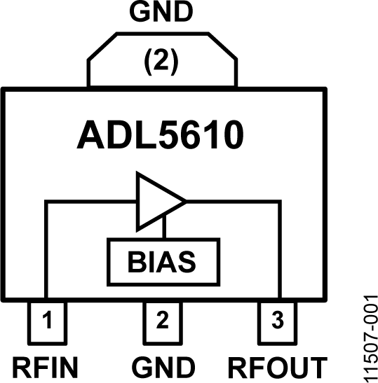
ADL5610-EVALZ
Analog Devices Inc.The ADL5610 is a single-ended RF/IF gain block amplifier that provides broadband operation from 30 MHz to 6 GHz. The ADL5610 provides a low noise figure of 2.2 dB with a very high OIP3 of more than 38 dBm simultaneously, which delivers a high dynamic range.?The ADL5610 provides a gain of 18 dB, which is stable over frequency, temperature, and power supply, and from device to device. The amplifier is offered in the industry-standard SOT-89 package and is internally matched to 50 ? at the input and output, making the ADL5610 easy to implement in a wide variety of applications. The only external parts required are the input and output ac coupling capacitors, power supply decoupling capacitors, and bias inductor.The ADL5610 has a high ESD rating of ?1.5 kV (Class 1C) and is fully specified for operation across a wide temperature range of ?40?C to +105?C.?A fully populated RoHS-compliant evaluation board is available.

ADL5611-EVALZ
Analog Devices Inc.The ADL5611 is a single-ended RF/IF gain block amplifier that provides broadband operation from 30 MHz to 6 GHz. The ADL5611 provides a low noise figure of 2.1 dB with a very high OIP3 of 40.0 dBm simultaneously, which delivers a high dynamic range.The ADL5611 provides a gain of 22.2 dB that is stable over frequency, temperature, and power supply, and from device to device. The amplifier is offered in the industry-standard SOT-89 package and is internally matched to 50?? at the input and output, making the ADL5611 easy to implement in a wide variety of applications. The only external parts required are the input and output ac coupling capacitors, power supply decoupling capacitors, and bias inductor.The ADL5611 has a high ESD rating of ?1.5 kV (Class 1C) and is fully specified for operation across a wide temperature range of ?40?C to +105?C. A fully populated RoHS-compliant evaluation board is available.

ADL5801-EVALZ
Analog Devices Inc.The ADL5801 uses a high linearity, doubly balanced, active mixer core with integrated LO buffer amplifier to provide high dynamic range frequency conversion from 10 MHz to 6 GHz. The mixer benefits from a proprietary linearization architecture that provides enhanced input IP3 performance when subject to high input levels. A bias adjust feature allows the input linearity, SSB noise figure, and dc current to be optimized using a single control pin. An optional input power detector is provided for adaptive bias control. The high input linearity allows the device to be used in demanding cellular applications where in-band blocking signals may otherwise result in degradation in dynamic performance. The adaptive bias feature allows the part to provide high input IP3 performance when presented with large blocking signals. When blockers are removed, the ADL5801 can automatically bias down to provide low noise figure and low power consumption.The balanced active mixer arrangement provides superb LO-to-RF and LO-to-IF leakage, typically better than ?40 dBm. The IF outputs are designed to provide a typical voltage conversion gain of 7.8 dB when loaded into a 200 ? load. The broad frequency range of the open-collector IF outputs allows the ADL5801 to be applied as an upconverter for various transmit applications.The ADL5801 is fabricated using a SiGe high performance IC process. The device is available in a compact 4 mm ? 4 mm, 24-lead LFCSP package and operates over a ?40?C to +85?C temperature range. An evaluation board is also available.APPLICATIONS Cellular base station receivers Radio link downconverters Broadband block conversion Instrumentation

ADL5903-EVALZ
Analog Devices Inc.The ADL5903 is a true rms responding power detector that has a 35 dB measurement range. It features low power consumption and an intrinsically ripple-free error transfer function.The ADL5903 provides a solution in a variety of high frequency systems requiring an accurate measurement of signal power. Requiring only a single supply of 3.0 V to 5.0 V and a few capacitors, it is easy to use and capable of being driven single-ended or with a balun for differential input drive. An on-chip matching network provides good return loss over the specified frequency range of the device. The ADL5903 can operate from 200 MHz to 6 GHz and can accept inputs from ?30 dBm to +20 dBm.The ADL5903 can be used to determine the true power of a high frequency signal with a complex modulation envelope including large crest factor signals such as GSM, CDMA, W-CDMA, TD-SCDMA, and LTE modulated signals. The output is then proportional to the logarithm of the rms value of the input. In other words, the reading is presented directly in decibels and is scaled about 35.5 mV/dB at 900 MHz.The ADL5903 has low power consumption when operational and a disable mode that further reduces the power consumption. Power consumption is less than 100 ?A when the ADL5903 enters power-down mode through a logic low at Pin ENBL. The ADL5903 is supplied in a 2 mm ? 2 mm, 8-lead LFCSP for operation over the wide temperature range of ?55?C to +125?C.Applications Power amplifier linearization/control loops Transmitter power controls Transmitter signal strength indication (TSSI) RF instrumentation Wireless repeaters

ADL5904-EVALZ
Analog Devices Inc.The ADL5904 is a dual-function radio frequency (RF) TruPwr? detector that operates from dc to 6 GHz. It provides rms power measurement along with a programmable envelope threshold detection function.The rms power measurement function has a 45 dB detection range, nominally from ?30 dBm to +15 dBm. The rms power measurement function features low power consumption and an intrinsically ripple free error transfer function.The envelope threshold detection function compares the voltage from an internal envelope detector with a user defined input voltage. When the voltage from the envelope detector exceeds the user defined threshold voltage, an internal comparator captures and latches the event to a set/reset (SR) flip flop. The response time from the RF input signal exceeding the user programmed threshold to the output latching is 12 ns. The latched event is held on the flip-flop until a reset pulse is applied.The RF input of the ADL5904 is dc-coupled, allowing operation down to arbitrarily low ac frequencies. It operates on a 3.3 V supply and consumes 3.5 mA. A disable mode reduces this current to 100 ?A when a logic low is applied to the ENBL pin.The ADL5904 is supplied in a 3 mm ? 3 mm, 16-lead LFCSP for operation over the wide temperature range of ?40?C to +105?C.Applications Transmitter signal strength indication (TSSI) Wireless power amplifier input and output protection Wireless receiver input protection

ADL5910-EVALZ
Analog Devices Inc.The ADL5910 is a radio frequency (RF) detector that operatesfrom dc to 6 GHz. It provides a programmable envelope threshold detection function.The envelope threshold detection function compares the voltagefrom an internal envelope detector with a user defined inputvoltage. When the voltage from the envelope detector exceedsthe user defined threshold voltage, an internal comparator captures and latches the event to a set or reset (SR) flip flop.The response time from the RF input signal exceeding the user programmed threshold to the output latching is 12 ns. The latchedevent is held on the flip flop until a reset pulse is applied.The RF input of the ADL5910 is dc-coupled, allowing operation down to arbitrarily low ac frequencies. It operates on a 3.3 Vsupply and consumes 3.5 mA. Power-down mode reduces thiscurrent to 100 ?A when a logic low is applied to the ENBL pin.The ADL5910 is supplied in a 3 mm ? 3 mm, 16-lead LFCSP for operation over the wide temperature range of ?40?C to +105?C.Applications Wireless power amplifier input and output protection Wireless receiver input protection RF pulse detection and triggering

ADL6012-EVALZ
Analog Devices Inc.The ADL6012 is a versatile, broadband envelope detector that operates from 2 GHz to 67 GHz. The combination of a wide, 500 MHz envelope bandwidth and a fast, 0.6 ns rise time makes the device suitable for a wide range of applications, including wideband envelope tracking, transmitter local oscillator (LO) leakage corrections, and high resolution pulse (radar) detection.The response of the ADL6012 is stable over a wide frequency range and features excellent temperature stability. Enabled by propriety technology, the device independently detects the positive and the negative envelopes of the RF input. Even order distortion at the RF input due to nonlinear source loading is also reduced when compared to classic diode detector architectures.The quasi differential output interface formed by the VENV+ and VENV? pins has a matched, 100 ? differential output impedance designed to drive a 100 ? differential load and up to 2 pF of capacitance to ground on each output. The output interface provides the detected and amplified positive and negative envelopes, which are level shifted using an externally applied voltage to the VOCM interface. This configuration simplifies interfacing to a high speed analog-to-digital converter (ADC).The ADL6012 is specified for operation from ?55?C to +125?C, and is available in a 10-lead, 3 mm ? 2 mm LFCSP.Applications Envelope tracking Microwave point to point links Microwave instrumentation Military radios Pulse radar receivers Wideband power amplifier linearization

ADL8107-EVALZ
Analog Devices Inc.The ADL8107 is a gallium arsenide (GaAs), monolithic microwave IC (MMIC), pseudomorphic high electron mobility transistor (pHEMT), low noise, wideband, high linearity amplifier that operates from 6 GHz to 18 GHz.The ADL8107 provides a typical gain of 24 dB at 7 GHz to 16 GHz, a 1.3 dB typical noise figure at 7 GHz to 16 GHz, a 18.5 dBm typical output power for 1 dB compression (OP1dB) at 7 GHz to 16 GHz, and a typical output third-order intercept (OIP3) of 29 dBm at 7 GHz to 16 GHz, requiring only 90 mA from a 5 V drain supply voltage. This low noise amplifier has a high output second-order intercept (OIP2) of 30.5 dBm typical at 7 GHz to 16 GHz, making the ADL8107 suitable for military and test instrumentation applications.The ADL8107 also features inputs and outputs that are internally matched to 50 ?. The RFIN and RFOUT pins are internally ac-coupled, and the bias inductor is also integrated, making the ADL8107 ideal for surface-mounted technology (SMT)-based, high density applications.The ADL8107 is housed in a RoHS-compliant, 2 mm ? 2 mm, 8-lead LFCSP.APPLICATIONSTest instrumentationMilitary communicationsRadar

ADL9005-EVALZ
Analog Devices Inc.The ADL9005 is a gallium arsenide (GaAs), monolithic microwave integrated circuit (MMIC), pseudomorphic high electron mobility transistor (pHEMT), wideband, LNA that operates from 0.01 to 26.5 GHz. The ADL9005 provides a typical gain of 17.5 dB from 0.01 GHz to 14 GHz with a positive gain slope from 14 GHz to 20 GHz, a 13.5 dBm typical output power at 1 dB compression (OP1dB) from 0.01 GHz to 20 GHz, a 2.5 dB typical noise figure from 0.01 GHz to 14 GHz, and a typical output third-order intercept (OIP3) of 26 dBm from 0.01 GHz to 14 GHz, requiring only 80 mA from a 5 V supply voltage. The saturated output power (PSAT) of up to 16 dBm enables the LNA to function as a local oscillator (LO) driver for many of Analog Devices, Inc., balanced, inphase/quadrature (I/Q) or image rejection mixers. The ADL9005 also features inputs and outputs (I/Os) that are internally matched to 50 ?, making it ideal for surface-mounted technology (SMT)-based, high capacity microwave radio applications.The ADL9005 is housed in a RoHS-compliant, 4 mm ? 4 mm, LFCSP.Multifunction pin names may be referenced by their relevant function only.APPLICATIONSTest instrumentationMilitaryCommunications

ADM1270RQ-EVALZ
Analog Devices Inc.The ADM1270 is a current-limiting controller that providesinrush current limiting and overcurrent protection for modularor battery-powered systems. When circuit boards are insertedinto a live backplane, discharged supply bypass capacitors drawlarge transient currents from the backplane power bus as theycharge. These transient currents can cause permanent damageto connector pins, as well as dips on the backplane supply thatcan reset other boards in the system.The ADM1270 is designed to control the inrush current, whenpowering on the system, via an external P-channel field effecttransistor (FET).To protect the system from a reverse polarity input supply, thereis a provision made to control an additional external P-channelFET. This feature prevents reverse current flow in case of a reversepolarity connection, which can damage the load or the ADM1270.The ADM1270 is available in a 3 mm ? 3 mm, 16-lead LFCSP anda 16-lead QSOP. Applications Industrial modules Battery-powered/portable instrumentation

ADM7150CP-EVALZ
Analog Devices Inc.The ADM7150 is a low dropout linear regulator that operates from 4.5 V to 16 V and provides up to 800 mA of output current. Using an advanced proprietary architecture, they provide high power supply rejection, low noise, and achieve excellent line and loadtransient response with a 10 ?F ceramic output capacitor.The ADM7150 is available in 1.8 V, 2.8 V, 3.0 V, 3.3 V and 5.0 V fixed output. 16 fixed output voltages between 1.5 V and 5.0 V are available upon request.The ADM7150 regulator typical output noise is 1.0 ?Vrms from 100Hz to 100KHz for fixed output voltage options and

ADM7155CP-02-EVALZ
Analog Devices Inc.The ADM7155 is an adjustable linear regulator that operates from 2.3 V to 5.5 V and provides up to 600 mA of load current. Output voltages from 1.2 V to 3.4 V are possible depending on the model. Using an advanced proprietary architecture, it provides high power supply rejection and ultralow noise, achieving excellent line and load transient response with only a 10 ?F ceramic output capacitor.The ADM7155 is available in four models that optimize power dissipation and PSRR performance as a function of input and output voltage. The ADM7155 regulator typical output noise is 0.9 ?V rms from 100 Hz to 100 kHz for fixed output voltage options and 1.5 nV/?Hz for noise spectral density from 10 kHz to 1 MHz. The ADM7155?is available in 8-lead, 3 mm ? 3 mm LFCSP and 8-lead SOIC?packages, making it not only a very compact solution but also?providing excellent thermal performance for applications requiring?up to 600 mA of load current in a small, low profile footprint.Applications Regulation to noise sensitive applications: PLLs, VCOs, and PLLs with integrated VCOs Communications and infrastructure Backhaul and microwave links

ADM8612-EVALZ
Analog Devices Inc.The ADM8611 /?ADM8612?/?ADM8613?/?ADM8614?/?ADM8615?are voltage supervisory circuits that monitor power supply voltage levels and code execution integrity in microprocessor-based systems. Apart from providing power-on reset signals, an on-chip watchdog timer can reset the microprocessor if it fails to strobe within a preset timeout period. A reset signal can also be asserted by an external push-button through a manual reset input.The ultralow power consumption of these devices makes them suitable for power efficiency sensitive systems, such as battery-powered portable devices and energy meters.The features of each member of the device family are shown in Table 9 in the data sheet. Each device subdivides into submodels with differences in factory preset voltage monitoring threshold options. In the range of 2 V to 4.63 V, 10 options are available for the ADM8611. In the range of 2.32 V to 4.63 V, five options are available for both the ADM8613 and ADM8614. A separate supply input allows the ADM8612 and ADM8615 to monitor 20 different low voltage levels from 0.5 V to 1.9 V. Not all device options are available as standard models.The ADM8611, ADM8612, ADM8613, and ADM8615 can reset on demand through the manual reset input. The watchdog function on the ADM8613, ADM8614, and ADM8615 monitors the heartbeat of the microprocessor through the WDI pin. The ADM8613 and ADM8614 have a watchdog disable input, which allows the user to disable the watchdog function, if required. The ADM8614 also has a watchdog timeout extension input, allowing the watchdog timeout to be extended from 1.6 sec to 100 sec.The ADM8611/ADM8612/ADM8613/ADM8614/ADM8615 are available in a 6-ball, 1.46 mm ? 0.96 mm WLCSP. These devices are specified over the temperature range of ?40?C to +85?C.??APPLICATIONS Portable/battery-operated equipment Microprocessor systems Energy metering Energy harvesting

ADM8843EB-EVALZ
Analog Devices Inc.The ADM8843 uses charge pump technology to provide thepower to drive up to four LEDs. The LEDs are used for backlightinga color LCD display that has regulated constant currentfor uniform brightness intensity. The main display can use up tothree LEDs, and the sub display uses one LED. The CTRL1 andCTRL2 digital input control pins control the shutdown operationand the brightness of the main and sub displays.To maximize power efficiency, the charge pump can operate in1?, 1.5?, or 2? mode. The charge pump automatically switchesamong 1?/1.5?/2? modes, based on the input voltage, tomaintain sufficient drive for the LED anodes at the highestpower efficiency.Improved brightness matching of the LEDs is achieved by afeedback pin that senses individual LED current with a typicalmatching accuracy of 0.3%.Applications Cellular phones with main and sub displays White LED backlighting Camera flash/strobes and movie light applications Micro TFT color displays DSC PDAs

ADMV1009-EVALZ
Analog Devices Inc.The ADMV1009 is a compact, gallium arsenide (GaAs) design,monolithic microwave integrated circuit (MMIC), upper sideband(USB), differential, upconverter in a RoHS compliant packageoptimized for point to point microwave radio designs thatoperate in the 12.7 GHz to 15.4 GHz frequency range.The ADMV1009 provides 21 dB of conversion gain with 20 dBof sideband rejection. The ADMV1009 uses a radio frequency (RF)amplifier preceded by a passive, double balanced mixer, where adriver amplifier drives the local oscillator (LO). IF1 and IF2 mixerinputs are provided, and an external 180? balun is needed todrive the IF pins differentially. The ADMV1009 is a muchsmaller alternative to hybrid style single sideband (SSB)upconverter assemblies and eliminates the need for wirebonding by allowing the use of surface-mount manufacturingassemblies.The ADMV1009 upconverter comes in a compact, thermallyenhanced, 4.9 mm ? 4.9 mm LCC package. The ADMV1009operates over the ?40?C to +85?C temperature range.Applications Point to point microwave radios Radars and electronic warfare systems Instrumentation, automatic test equipment

ADMV1128IQ-EVALZ
Analog Devices Inc.The ADMV1128 is a silicon on isolator (SOI), microwave, upconverter and downconverter optimized for 5G radio designs operating in the 24 GHz to 29.5 GHz frequency range.Both upconverters and downconverters offer two modes of frequency translation. One mode is conversion from and/or to single-ended or complex intermediate frequency (IF) signals, which then pass through an on-chip 90? IF hybrid, known as IF mode.The other mode is a direct conversion from and/or to differential baseband inphase/quadrature (I/Q) inputs and outputs, known as baseband mode. The I/Q baseband output common-mode voltage is programmable between 0 V and 1.5 V. The SPI provides fine adjustment of the quadrature phase to optimize I/Q demodulation performance.When the device is used as an image rejecting downconverter, the unwanted image term is typically rejected to 24 dBc, before calibration. The ADMV1128 offers a square law power detector to allow monitoring of the power levels at the mixer inputs of the downconverter.The RF receive input, RF transmit output, and local oscillator (LO) interface are all single-ended and matched to 50 ?. The on-chip RF switch provides the option to combine the transmit and receive RF ports together for time division duplex (TDD) applications. The serial port interface (SPI) provides adjustment of the quadrature phase to allow optimum sideband rejection. In addition, the SPI allows powering down the output envelope detector to reduce power consumption when carrier feedthrough optimization is not necessary.The ADMV1128 upconverter and downconverter is housed in a compact, thermally enhanced, 6 mm ? 6.5 mm, ball grid array (BGA) package. This BGA package enables the ability to heat sink the ADMV1128 from the top of the package for the most efficient thermal heat sinking. The ADMV1128 operates over the ?40?C to +95?C TC range.APPLICATIONS Millimeter-wave 5G applications Point to point microwave radios Radar and electronic warfare systems Instrumentation and automatic test equipment (ATE)

ADMV7410-EVALZ
Analog Devices Inc.The ADMV7410 is a fully integrated system in package (SiP)in phase/quadrature (I/Q) downconverter that operatesbetween an intermediate frequency (IF) output range of dc and2 GHz and a radio frequency (RF) input range of 71 GHz and76 GHz. The device provides a small signal conversion gain of13 dB with 30 dBc of image rejection. The ADMV7410 uses alow noise amplifier followed by an image rejection mixer that isdriven by a 6? local oscillator (LO) multiplier. Differential Iand Q mixer outputs are provided for direct conversionapplications. Alternatively, the outputs can be combined usingan external 90? hybrid and two external 180? hybrids for single-ended applications. The ADMV7410 comes in a fully integrated, surface-mount,34-terminal, 11 mm ? 13 mm, chip array small outline no leadcavity (LGA_CAV) package. The ADMV7410 operates over the?40?C to +85?C case temperature range.APPLICATIONS E-band communication systems High capacity wireless backhauls Test and measurement Aerospace and defense

ADMV8416-EVALZ
Analog Devices Inc.The ADMV8416 is a monolithic microwave integrated circuit (MMIC), tunable band-pass filter that features a user selectable pass-band frequency. The 3 dB filter bandwidth is approximately 15% of the center frequency (fCENTER), and the 20 dB filter bandwidth is 37%. Additionally, fCENTER can be varied between 6.8 GHz to 16.8 GHz by applying an analog fCENTER tuning voltage between 0 V to 15 V. The usable pass band corner frequencies (fCORNER) span from 6.3 GHz to 18 GHz. This tunable filter can be used as a much smaller alternative to large switched filter banks and cavity tuned filters. The filter has excellent microphonics due to the monolithic design and provides a dynamically adjustable solution.Applications Test and measurement equipment Military radar and electronic warfare (EW) systems Video satellite (VSAT) communications

ADMV8420-EVALZ
Analog Devices Inc.ADMV8420ACPZThe ADMV8420 is a monolithic microwave integrated circuit (MMIC), tunable band-pass filter that features a user-selectable pass band frequency. The 3 dB filter bandwidth is approximately 20%, and the 20 dB filter bandwidth is approximately 40%. Additionally, the center frequency (fCENTER) varies between 11.1 GHz to 19.6 GHz by applying a center frequency control voltage between 0 V to 15 V. The usable pass band corner frequencies (fCORNER) span from 10 GHz to 21.7 GHz. This tunable filter is a smaller alternative to switched filter banks and cavity tuned filters. The ADMV8420 has minimal microphonics due to the monolithic design and provides a dynamically adjustable solution in advanced communications applications.ADMV8420CHIPSThe ADMV8420 is a monolithic microwave IC (MMIC), tunable band-pass filter (BPF) that features a user?selectable pass band frequency. The 3 dB filter bandwidth is approximately 20%, and the 20 dB filter bandwidth is approximately 40%. Additionally, the center frequency (fCENTER) varies between 10.5 GHz to 21 GHz by applying a center frequency control voltage (VFCTL) between 0 V to 15 V. The usable pass band 3 dB corner frequency (f3dB) spans from 10 GHz to 22.8 GHz. This tunable filter is a smaller alternative to switched filter banks and cavity tuned filters. The ADMV8420 has minimal microphonics due to the monolithic design and provides a dynamically adjustable solution in advanced communications applications.Applications Test and measurement equipment Military radar and electronic warfare systems Very small aperture terminal (VSAT) communications Airport scanners

ADMV8526-EVALZ
Analog Devices Inc.The ADMV8526 is an RF band-pass filter that features a digitally selectable frequency of operation. The filter center frequency (fCENTER) can be adjusted from 1.25 GHz to 2.60 GHz, using an 8-bit value (256 states) that incorporates a patent pending interpolation technique.The typical 3 dB bandwidth is 9% and adjustability is ?2%. Insertion loss is typically 4 dB, and the 20 dB rejection is 16% away from fCENTER, which is ideally suited for minimizing system interferers.This tunable filter can be used as a smaller alternative to large switched filter banks and discrete component-based tunable filters, and this device provides a dynamically adjustable solution in advanced communications applications.


